

PD55025
PD55025S
RF POWER TRANSISTORS
N-CHANNEL ENHANCEMENT-MODE LATERAL
MOSFETs
• EXCELLENT THERMAL STABILITY
• COMMON SOURCE CONFIGURATION
• P
= 25 W with 14.5 dB gain @ 500 MHz /
OUT
12.5 V
• NEW RF PLASTIC PACKAGE
DESCRIPTION
The PD55025 is a common source N-Channel,
enhancement-mode lateral Field-Effect RF power
transistor. It is designed for high gain, broad band
commercial and industrial applications. It operates
at 12 V in common source mode at frequencies of
up to 1 GHz. PD 55025 boasts the excellent gain,
linearity and reliability of ST’s latest LDMOS
technology mounted in the first true SMD pla stic
RF power package, PowerSO-10RF . PD55025’s
superior linearity performance makes it an ideal
solution for car mobile radio.
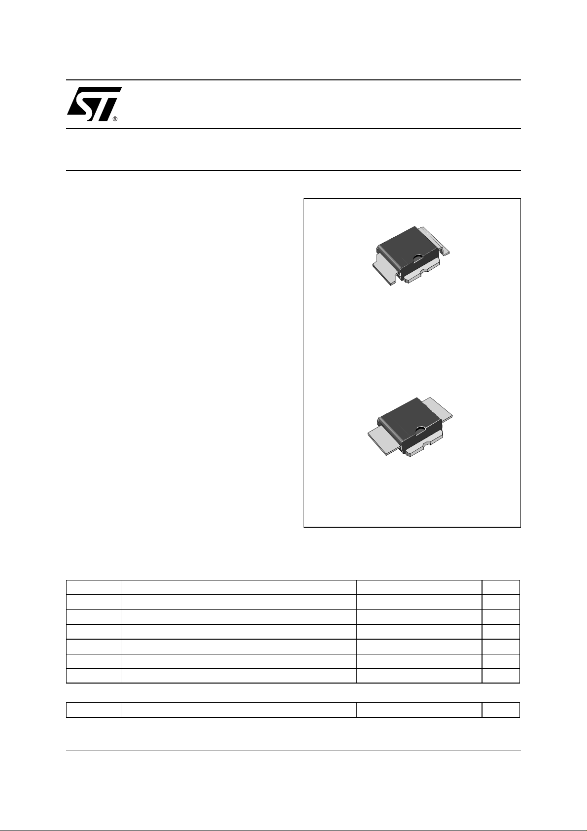
The LdmoST
PowerSO-10RF
(formed lead)
ORDER CODE
PD55025
Plastic FAMILY
BRANDING
PD55025
The PowerSO-10 plastic package, designed to
offer high reliability, is the first ST JEDEC
approved, high power SM D package. I t has b een
specially optimized for RF needs and offers
excellent RF performances and ease of assembly.
ORDER CODE
PD55025S
PowerSO-10R F
(straight lead)
BRANDING
PD55025S
Mounting recommendations are available in
www.st.com/rf/ (look for application note AN1294)
ABSOLUTE MAXIMUM RATINGS (T
Symbol Parameter Value Unit
V
(BR)DSS
V
GS
I
D
P
DISS
Tj Max. Operating Junction Temperature 165 °C
T
STG
Drain-Source Voltage 40 V
Gate-Source Voltage ± 20 V
Drain Current 7 A
Power Dissipation (@ Tc = 70°C) 79 W
Storage Temperature -65 to +150 °C
CASE
= 25°C)
THERMA L D ATA
R
th(j-c)
Junction -Case Thermal Resistance 1.2 °C/W
1/13March, 21 2003
PD55025 - PD55025S
ELECTRICAL SPECIFICATION (T
CASE
= 25°C)
STATIC
Symbol Test Conditions Min. Typ. Max. Unit
I
DSS
I
GSS
V
GS(Q)
V
DS(ON)
G
C
C
C
FS
ISS
OSS
RSS
VGS = 0 V VDS = 28 V
VGS = 20 V VDS = 0 V
VDS = 28 V
= 100 mA
ID
VGS = 10 V ID = 3 A
VDS = 10 V ID = 3 A
VGS = 0 V VDS = 12.5 V f = 1 MHz
VGS = 0 V VDS = 12.5 V f = 1 MHz
VGS = 0 V VDS = 12.5 V f = 1 MHz
1 µA
1 µA
2.0 5.0 V
0.7 0.8 V
2.5 mho
86 pF
76 pF
5.8 pF
DYNAMIC
Symbol Test Conditions Min. Typ. Max. Unit
P
out
G
P
η
D
Load
mismatch
VDD = 12.5 V IDQ = 200 mA f = 500 MHz
VDD = 12.5 V IDQ = 200 mA P
VDD = 12.5 V IDQ = 200 mA P
= 12.5 V IDQ = 200 mA P
V
DD
= 25 W f = 500 MHz
OUT
= 25 W f = 500 MHz
OUT
= 25 W f = 500 MHz
OUT
ALL PHASE ANGLES
25 W
14.5 dB
50 %
20:1 VSWR
GATE
SC15200
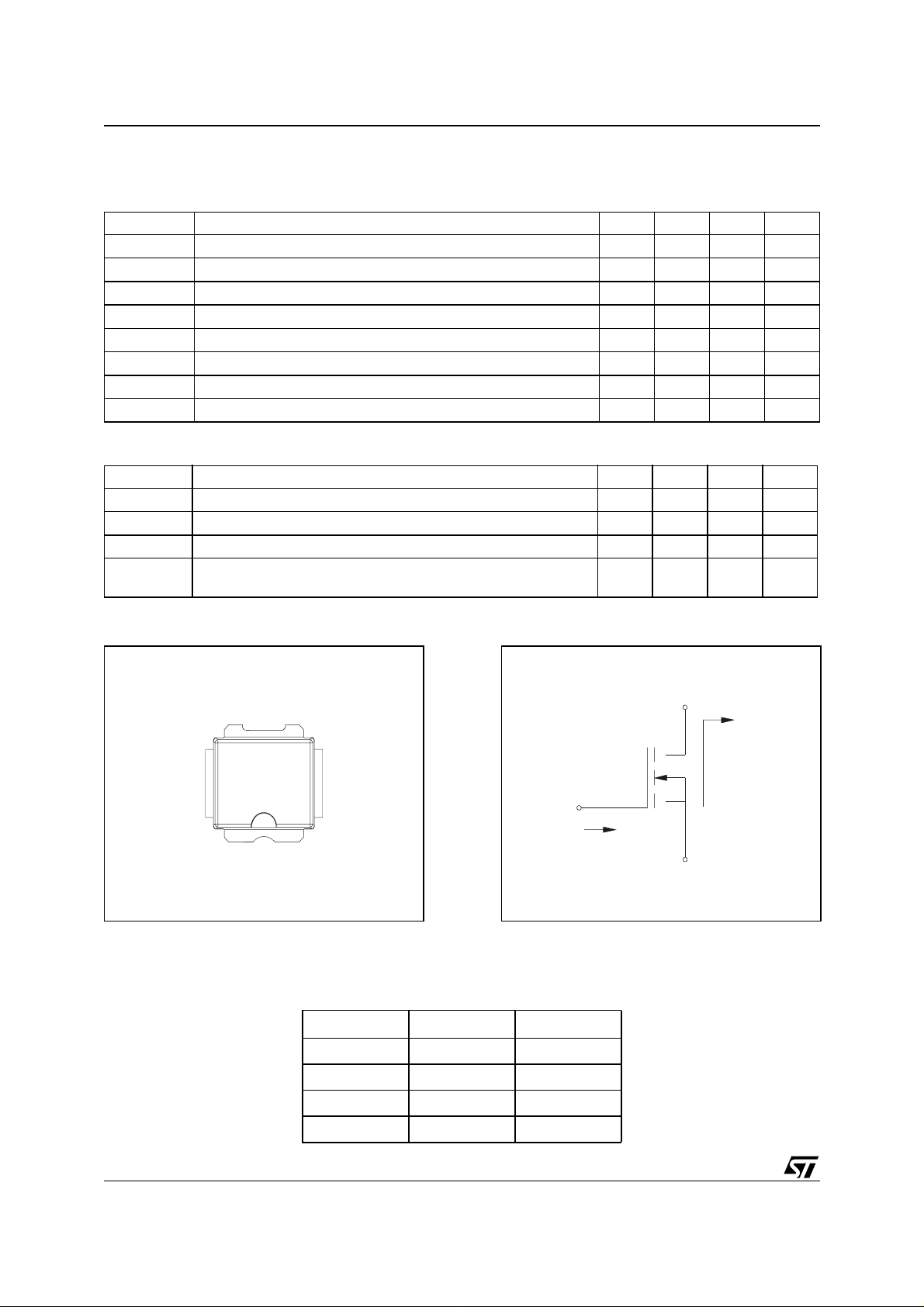
PIN CONNECTION
PD55025S
SOURCE
DRAIN
SC13140
IMPEDANCE DATA
Z
FREQ. MHz
175 3.20 - j 4.41 1.56 + j 2.14
480 1.01 - j 1.67 1.06 + j 0.22
500 0.93 - j 1.53 1.12 + j 0.20
(Ω)Z
IN
Typical Input
Impeda nce
G
Zin
(Ω)
DL
D
Z
Typical Drain
Load Imped ance
S
DL
2/13
520 0.88 - j 1.98 1.07 + j 0.83
TYPICAL PERFORMANCE
q
Capacitance vs. Supply Voltage
1000
Ciss
100
Coss
C (pF)
(PD55025S)
PD55025 - PD55025S
Drain Current vs Gate-Source Voltage
6
Vds = 10 V
5
4
3
Id (A)
10
Crss
f = 1 MHz
1
0 4 8 1216202428
Vds (V)
Gate-Source Voltage vs Case Temperature
1.04
1.02
Id = 5 A
1.00
Id (A)
0.98
0.96
Vds = 10 V
0.94
-25 0 25 50 75 100
Vgs (V)
Id = 4 A
Id = 3 A
Id = 2 A
Id = 1 A
Id = .5 A
2
1
0
2.0 2.5 3.0 3.5 4.0 4.5 5.0 5.5
Vgs (V)
Output Power vs Input Power
45
40
35
30
25
20
Pout (W)
15
10
5
0
0.00 1.00 2.00 3.00 4.00 5.00 6.00
480 MH z
Pin (W)
500 MHz
520 MHz
Vdd = 12.5 V
Id
= 200 mA
Output Power vs Input Power
45
40
35
30
25
20
Pout (W)
15
10
Vdd = 13.8 V
Vdd = 12 .5 V
5
0
0123456
Pin (W)
f = 520 MHz
Idq = 200 mA
Powe r Ga i n vs Outpu t Pow er
18
16
14
12
10
Gp (dB)
8
6
4
2
0
0 1020304050
Pout (W)
520 MHz
Vdd = 12.5 V
Idq = 200 mA
480 MHz
500 MHz
3/13

PD55025 - PD55025S
TYPICAL PERFORMANCE
Drain Efficiency vs Output Power
(PD55025S)
Input Return Loss vs Output Power
70
60
50
40
Nd (%)
30
20
10
0
0 1020304050
500 MHz
480, 520 MHz
Pout (W)
Vdd = 12.5 V
Idq = 200 mA
Output Power vs Bias Curent
40
35
30
25
20
Pout (W)
15
10
5
0
0 200 400 600 800 100 0 1200
Idq (m A)
480 MHz
520 MHz
Vdd = 12.5 V
Pin = 0.85 W
500 MHz
0
-5
-10
-15
-20
RL (dB)
-25
-30
-35
-40
0 1020304050
480 MHz
500 MHz
520 MHz
Pout (W)
Vdd = 12.5 V
Idq = 200 mA
Drain Efficiency vs Bias Current
60
50
40
30
Nd (%)
20
10
0
0 200 400 600 800 1000 1200
Idq ( m A)
500 MHz
520 MHz
Vdd = 12.5 V
Pin = 0 . 85 W
480 MH z
Output Power vs Supply Voltage
35
30
25
20
Pout (W)
15
10
5
0
5 7 9 1113151719
Vdd ( V)
4/13
520 MHz
480 MHz
500 MHz
I dq = 200 mA
Pin = 0.85 W
Drain Efficiency vs Supply Voltage
70
60
50
40
Nd (%)
30
20
10
0
6 8 10 12 14 16 18
500 MHz
500 MHz
520 MHz
Vdd (V)
Idq = 200 mA
Pin = 0.85 W
 Loading...