

RF & MICROWAVE TRAN SIST ORS
.REFRACTORY/GOLD METALLIZATION
.EMITTER SITE BALLASTED
.
:1 VSWR CAPABILITY
∞
.LOW THERMAL RESISTANCE
.INPUT MATCHING
.OVERLAY GEOMETRY
.METAL/CERAMIC HERMETIC PACKAGE
.P
OUT =
35 W MIN. WITH 10.7 dB GAIN
MSC81035M
AVIONI CS APPLICAT IONS
.280 2LF L (S06 8)
epoxysealed
ORDER CODE
MSC81035M
BRANDING
81035M
DESCRIPTI ON
The MSC81035M is a medium power Class C
transistor designed specifically for pulsed L-Band
avionics applications. This device is a direct replacement for the MSC1035M. MSC81035M offers improved saturated ouput power and collector efficiency based on the test circuit described
herein.
Low RF thermal resistance and computerized automatic wire bonding techniques ensure high reliability and product consistency.
The MSC8103 5M is housed in t he IMPAC
package with internal input matching.
ABSOLUTE MAXIMUM RATINGS (T
Symbol Parameter Value Uni t
P
T
DISS
I
V
CC
T
STG
C
J
Power Dissipation* (TC≤ 100°C) 150 W
Device Current* 3.0 A
Collector-Supply Voltage* 55 V
Junction Temperature (Pulsed RF Operation) 250
Storage Temperature
case
= 25°C)
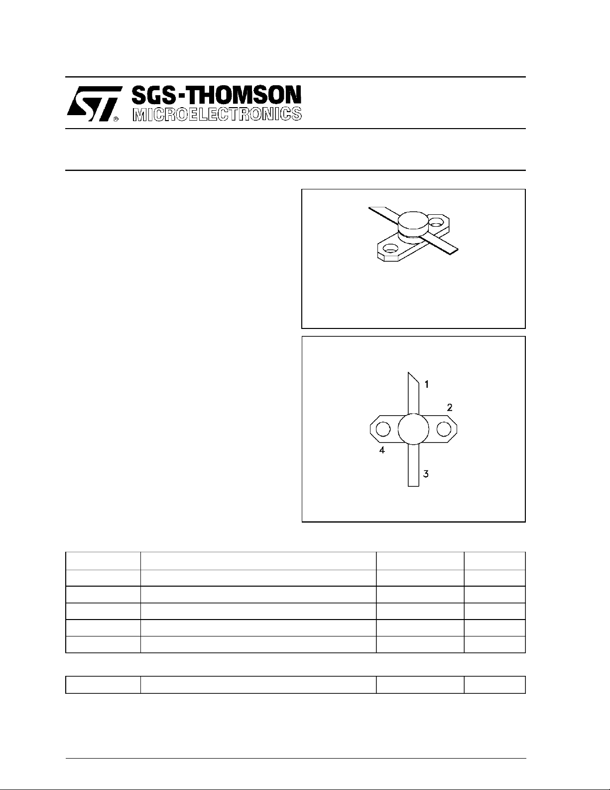
PIN CONNECTION
1. Collector 3. Emitter
2. Base 4. Base
65 to +200
−
°
C
°
C
THERMA L DA TA
R
TH(j-c)
*Appliesonly to rated RF amplifieroperation
Note: Thermal Resistancedetermined by Infra-RedScanning of Hot-Spot
September 2, 1994
Junction Temperature at ratedRF operatingconditions.
Junction-Case Thermal Resistance* 1.0
°
C/W
1/4
MS C8 1 035M
ELECTRICAL SPECIFICATIO NS (T
case
= 25°C)
STATIC
Symbol Test Conditions
BV
CBOIC
BV
EBOIE
BV
CERIC
I
CES
h
FE
= 10 mA IE= 0mA 65 — — V
= 1mA IC=0 mA 3.5 — — V
= 10 mA RBE= 10 Ω 65 — — V
VBE= 0V VCE= 50 V — — 5 mA
VCE= 5V IC=500 mA 15 — 120 —
DYNAMIC
Symbol Test Cond itions
P
OUT
η
P
Note: Pulse Width
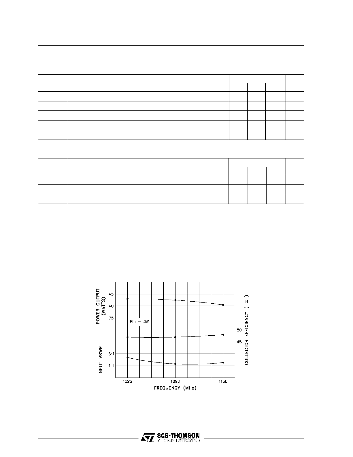
f = 1025 − 1150 MHz P
cf=1025 − 1150 MHz P
f = 1025 − 1150 MHz P
G
10µSec
=
Duty Cycle=1%
3.0 W V
=
IN
3.0 W V
=
IN
3.0 W V
=
IN
Value
Min. Typ. M ax.
Value
Min. Typ. Max.
50 V 35 40 — W
=
CC
50 V 40 — — %
=
CC
50 V 10.7 11.2 — dB
=
CC
Unit
Unit
TYPICA L PERFO R MA NCE
TYPICAL BROADBAND POWER
AMPLIFIER
2/4

IMPEDA NCE DATA
TYPICAL INPUT
IMPEDANCE
Z
IN
TYPICAL COLLECTOR
LOAD IMPEDANCE
MSC81035M
Z
IN
H
M
Z
CL
L
FREQ. ZIN(Ω)Z
CL
L=1025 MHz 2.6 + j 8.3 7.7 + j 2.0
M=1090 MHz 2.8 + j 8.7 7.1 + j 1.0
H=1150 MHz 3.2 + j 4.4 6.5 − j 0.5
TEST CIRCUIT
Ref.: Dwg. No. 101 002888
(Ω)
Z
CL
L
M
H
P
3.0 W
=
IN
V
50 V
=
CC
Normalized to 50 ohms
All dimensions are in inches.
3/4

MS C8 1 035M
PACKAGE MECHANICAL DATA
Ref.: Dwg. No. 12-0218 rev. A
Information furnished is believed to be accurate and reliable. However, SGS-THOMSON Microelectronics assumes no responsibility
for the consequences of use of such information nor for any infringement of patents or other rights of third parties which may result
from its use. No license is granted by implication or otherwise under any patent or patent rights of SGS-THOMSON Microelectronics. Specifications mentioned in this publication are subject to change without notice. This publication supersedes and replaces all
information previously supplied. SGS-THOMSON Microelectronics products are not authorized for use as critical components in life
support devices or systems without express written approval of SGS-THOMSON Microelectronics.
1994 SGS-THOMSON Microelectronics - All Rights Reserved
Australia - Brazil - France - Germany - Hong Kong - Italy - Japan - Korea - Malaysia - Malta - Morocco - The Netherlands -
Singapore - Spain - Sweden - Switzerland - Taiwan - Thailand - United Kingdom - U.S.A.
SGS-THOMSON Microelectronics GROUP OF COMPANIES
4/4
 Loading...