

Datasheet M48Z02, M48Z12-150PC1, M48Z12, M48Z02-70PC1, M48Z02-200PC1 Datasheet (SGS Thomson Microelectronics)
...
16 Kbit (2Kb x 8) ZEROPOWER® SRAM
INTEGRATED ULTRA LOW POWER SRAM,
POWER-FAIL CONTROL CIRCUIT and
BATTERY
UNLIMITED WRITE CYCLES
READ CYCLE TIME EQUALS WRITE CYCLE
TIME
AUTOMATIC P OWER-F AIL CHIP DES ELECT and
WRITE PROTECTION
WRITE PROTECT VOLT AGES
= Power-fail Deselect Voltage):
(V
PFD
– M48Z02: 4.50V ≤ V
– M48Z12: 4.20V ≤ V
SELF-CONTAINED BATTERY in the CAPHAT
DIP PACKAGE
PIN and FUNCTION COMPATIBLE with
JEDEC STANDARD 2K x 8 SRAMs
DESCRIPTION
The M48Z02/12 ZEROPOWER
non-volatile static RAM which is pin and functional
compatible with the DS1220.
A special 24 pin 600mil DIP CAPHAT package
houses the M48Z02/12 silicon with a long life lithium button cell to form a highly integrated battery
backed-up memory solution.
The M48Z02/12 button cell has sufficient capacity
and storage life to maintain data and clock functionality for an accumulated time period of at least 10
years in the absence of power over the oper ating
temperature range.
T ab le 1. Signal Names
PFD
PFD
4.75V
≤
4.50V
≤
®
RAM is a 2K x 8
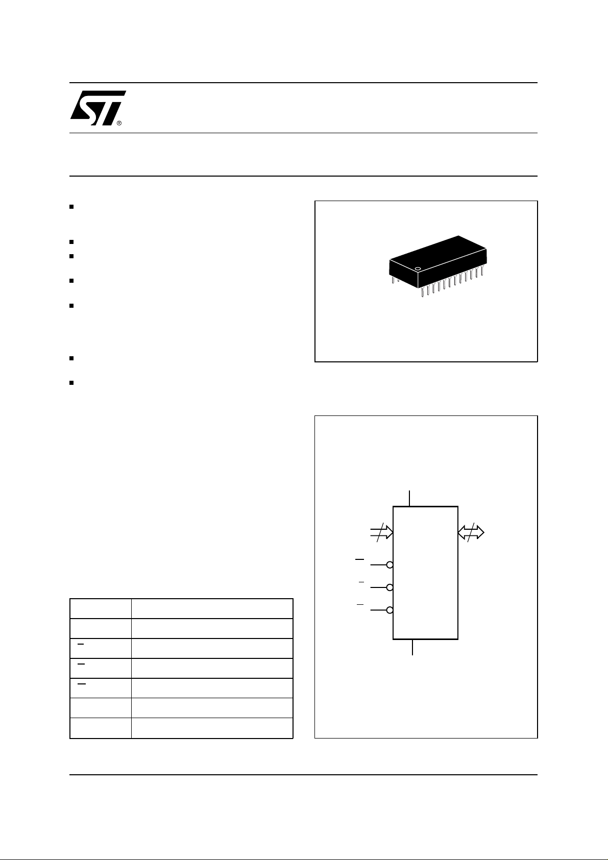
24
1
PCDIP24 (PC)
Battery CAPHAT
Figure 1. Logic Diagram
V
CC
11
A0-A10
W
E
M48Z02
M48Z12
M48Z02
M48Z12
8
DQ0-DQ7
A0-A10 Address Inputs
DQ0-DQ7 Data Inputs / Outputs
E Chip Enable
G Output Enable
W Write Enable
V
CC
V
SS
May 1999 1/12
Supply Voltage
Ground
G
V
SS
AI01186
M48Z02, M48Z12
T ab le 2. Absolute Maximum Ratings
(1)
Symbol Parameter Value Unit
T
A
T
STG
(2)
T
SLD
V
IO
V
CC
I
O
P
D
Notes:
1. Stresses greater than those listed under "Absolute Maximum Ratings" may cause permanent damage to the device. This is a
stress rating only and functional operation of the device at these or any other conditions above those indi cat ed in the operati onal
section of this specification is not implied. Exposure to the absolute maximum rating conditions for extended periods of time may
affect reliability.
2. Soldering temperature not to exceed 260°C for 10 seconds (total thermal budget not to exceed 150°C for longer than 30 seconds).
CAUTION: Negat i ve undershoots below –0.3 volts are not allowed on any pin while in the Battery Back-up mode.
Ambient Operating Temperature –40 to 85 °C
Storage T emper ature (VCC Off) –40 to 85 °C
Lead Solder Temperature for 10 seconds 260 °C
Input or Output Voltages –0.3 to 7 V
Supply Voltage –0.3 to 7 V
Output Current 20 mA
Power Dissipation 1 W
T ab le 3. Operating Modes
Mode V
CC
Deselect
Write V
Read V
4.75V to 5.5V
or
4.5V to 5.5V
Read V
Deselect V
Deselect ≤ V
Notes
: X = V
IH
to V
SO
or VIL; VSO = Battery Back-up Switchover Voltage.
(min) X X X High Z CMOS Standby
PFD
SO
E G W DQ0-DQ7 Power
V
IH
IL
IL
IL
X X High Z Standby
XVILD
V
IL
V
IH
V
IH
V
IH
IN
D
OUT
High Z Active
Active
Active
X X X High Z Battery Back-up Mode
Figure 2. DIP Pin Connections
24
23
22
21
20
19
18
17
16
15
14
13
AI01187
2/12
A7
A6
A5
A4
A3
A2
A1
A0
DQ0
DQ2
SS
1
2
3
4
5
6
7
8
9
10
11
12
M48Z02
M48Z12
V
CC
A8
A9
W
G
A10
E
DQ7
DQ6
DQ5DQ1
DQ4
DQ3V
DESCRIPTION
(cont’d)
The M48Z02/12 is a non-volatile pin and function
equivalent to any JEDEC standard 2K x 8 SRAM.
It also easily fits into many ROM, EPROM, and
EEPROM sockets, providing the non-volatility of
PROMs without any requirement for special write
timing or limitations on the number of writes that
can be performed.
The M48Z02/12 also has its own Power-fail Detect
circuit. The control circuitry constantly monitors the
single 5V supply for an out of tolerance condition.
When V
is out of tolerance, the circuit write
CC
protects the SRAM, providing a high degree of data
security in the midst of unpr edictable system operation brought on by low V
. As VCC falls below
CC
approximately 3V , the control circuitry connects the
battery which maintains data and clock operation
until valid power returns.
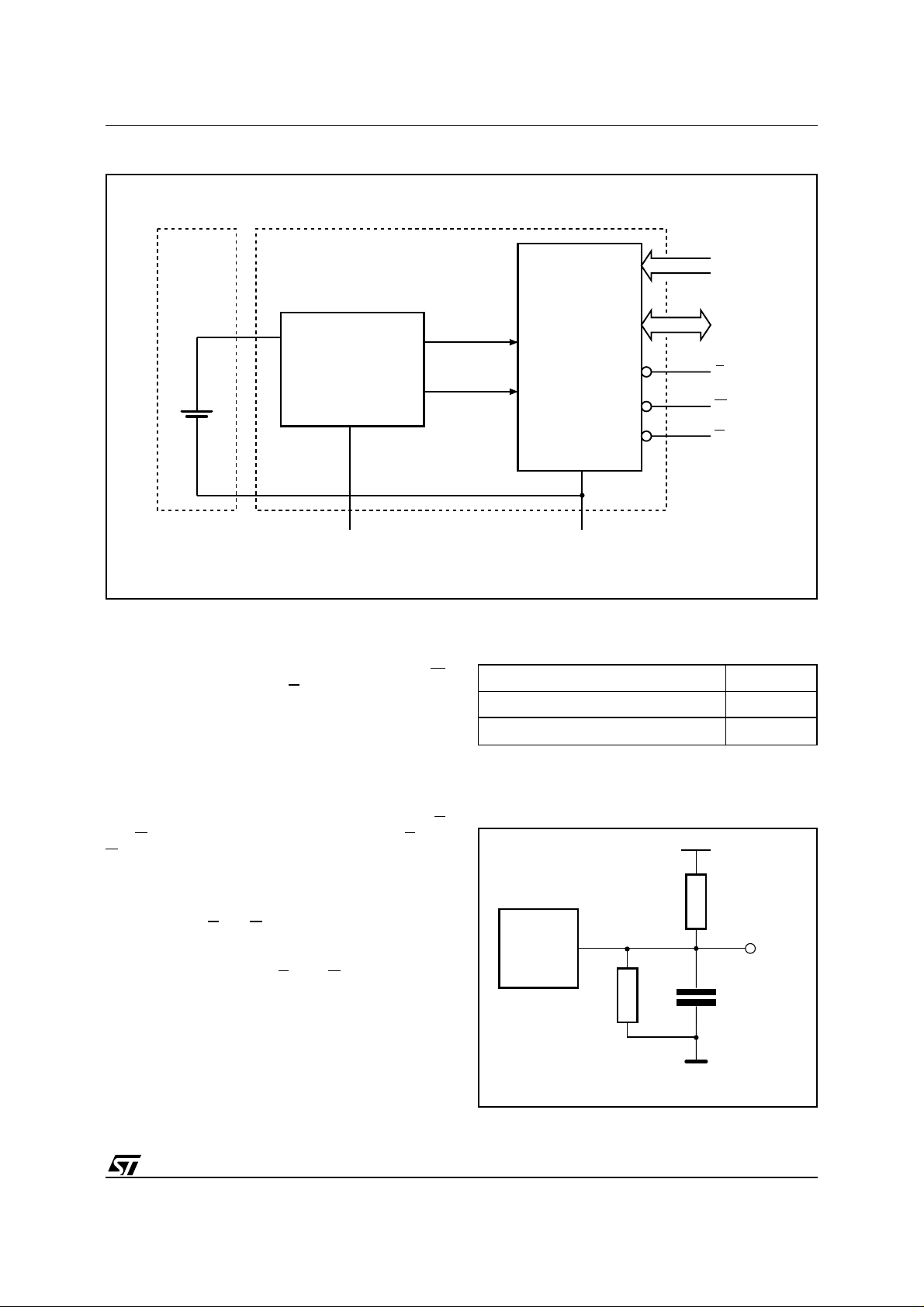
Figure 3. Block Diagram
M48Z02, M48Z12
A0-A10
LITHIUM
CELL
VOLTAGE SENSE
AND
SWITCHING
CIRCUITRY
V
CC
READ MODE
The M48Z02/12 is in the Read Mode whenever
(Write Enable) is high and
E (Chip Enable) is low.
W
The device architecture allows ripple-through access of data from eight of 16,384 locations in the
static storage array. Thus, the unique address
specified by the 11 Address Inputs defines which
one of the 2,048 bytes of data is to be accessed.
Valid data will be available at the Data I/O pins
within Address Access time (t
) after the last
AVQV
address input signal is stable, providing that the
G access times are also satisfied. If the E and
and
G access times are not met, valid data will be
available after the latter of the Chip Enable Access
time (t
) or Output Enable Access time (t
ELQV
GLQV
The state of the eight three-state Data I/O signals
is controlled by
before t
AVQ V
indeterminate state until t
puts are changed while
E and G. If the outputs are activated
, the data lines will be driven to an
. If the Address In-
AVQV
E and G remain active,
output data will remain valid for Output Data Hold
time (t
) but will go indeterminate until the next
AXQX
Addres s Access.
POWER
V
PFD
2K x 8
SRAM ARRAY
V
SS
Table 4. AC Measurement Conditions
Input Rise and Fall Times ≤ 5ns
Input Pulse Voltages 0V to 3V
Input and Output Timing Ref. Voltages 1.5V
Note that Output Hi-Z is defined as the point where data is no
longer driven.
Figure 4. AC Testing Load Circuit
E
).
DEVICE
UNDER
TEST
1kΩ
DQ0-DQ7
E
W
G
AI01255
5V
1.8kΩ
OUT
CL = 100pF
CL includes JIG capacitance
AI01019
3/12
M48Z02, M48Z12
(1)
T ab le 5. Capacitance
= 25 °C)
(T
A
Symbol Parameter T est Condition Min Max Unit
C
IN
(2)
C
IO
Notes:
1. Effective capacitance measured with power supply at 5V .
2. Outputs deselected
Input Capacitance VIN = 0V 10 pF
Input / Output Capacitance V
= 0V 10 pF
OUT
T ab le 6. DC Characteristics
= 0 to 70°C or –40 to 85°C; VCC = 4.75V to 5.5V or 4.5V to 5.5V)
(T
A
Symbol Parameter Test Condition Min Max Unit
(1)
I
LI
(1)
I
LO
Supply Current Outputs open 80 mA
I
CC
I
CC1
I
CC2
(2)
V
IL
V
IH
V
OL
V
OH
Notes:
1. Outputs Deselected.
2. Negative spikes of –1V allowed for up to 10ns once per cycle.
T able 7. Power Down/Up Trip Points DC Characteristics
= 0 to 70°C or –40 to 85°C)
(T
A
Input Leakage Current 0V ≤ VIN ≤ V
Output Leakage Current 0V ≤ V
Supply Current (Standby) TTL E = V
Supply Current (Standby) CMOS E = VCC – 0.2V 3 mA
OUT
≤ V
IH
CC
CC
Input Low Voltage –0.3 0.8 V
Input High Voltage 2.2 VCC + 0.3 V
Output Low Voltage IOL = 2.1mA 0.4 V
Output High Voltage IOH = –1mA 2.4 V
(1)
±1 µA
±5 µA
3mA
Symbol Parameter Min Typ Max Unit
V
PFD
V
PFD
V
SO
t
DR
Note:
1. All voltages referenced to V
Power-fail Deselect Voltage (M48Z02) 4.5 4.6 4.75 V
Power-fail Deselect Voltage (M48Z12) 4.2 4.3 4.5 V
Battery Back-up Switchover Voltage 3.0 V
Expected Data Retention Time 10 YEARS
4/12
.
SS

M48Z02, M48Z12
T able 8. Power Down/Up Mode AC Characteristics
= 0 to 70°C or –40 to 85°C)
(T
A
Symbol Parameter Min Max Unit
E or W at VIH before Power Down 0 µs
V
(max) to V
PFD
V
(min) to VSO VCC Fall Time 10 µs
PFD
V
(min) to V
PFD
VSO to V
PFD
(min) VCC Fall Time 300 µs
PFD
(max) VCC Rise Time 0 µs
PFD
(min) VCC Rise Time 1 µs
E or W at VIH after Power Up 2 ms
(max) to V
PFD
passes V
CC
(min) to VSO fall time of less than tFB may cause corruption of RAM data.
PFD
(min) fall time of less than tF may result in deselection/write protection not occurring until 50 µs after
PFD
(min).
PFD
Notes
t
PD
(1)
t
F
t
FB
t
R
t
RB
t
REC
:1.V
2. V
(2)
V
Figure 5. Power Down/Up Mode AC Waveforms
V
CC
V
(max)
PFD
V
(min)
PFD
VSO
tF
tDR
tFB
INPUTS
OUTPUTS
Note:
Inputs may or may not be recognized at this time. Caution should be taken to keep
may perform inadvertent writ e cyc l es after V
reset is being applied to the processor, a reset condition may not occur until after the system clock is running.
VALID VALID
(PER CONTROL INPUT)
rises above V
CC
(min) but before normal system operations begin. Even though a power on
PFD
DON'T CARE
HIGH-Z
E high as VCC rises past V
tR
NOTE
(PER CONTROL INPUT)
PFD
tRECtPD tRB
RECOGNIZEDRECOGNIZED
AI00606
(min ). Some system s
5/12

M48Z02, M48Z12
T ab le 9. Read Mode AC Characteristics
= 0 to 70°C or –40 to 85°C; VCC = 4.75V to 5.5V or 4.5V to 5.5V)
(T
A
Symbol Parameter
-70 -150 -200
Min Max Min Max Min Max
t
AVAV
t
AVQV
t
ELQV
t
GLQV
t
ELQX
t
GLQX
t
EHQZ
t
GHQZ
t
AXQX
Read Cycle Time 70 150 200 ns
Address Valid to Output Valid 70 150 200 ns
Chip Enable Low to Output Valid 70 150 200 ns
Output Enable Low to Output Valid 35 75 80 ns
Chip Enable Low to Output Transition 5 10 10 ns
Output Enable Low to Output Transition 5 5 5 ns
Chip Enable High to Output Hi-Z 25 35 40 ns
Output Enable High to Output Hi-Z 25 35 40 ns
Address Transition to Output Transition 10 5 5 ns
Figure 6. Read Mode AC Waveforms
M48Z02 / M48Z12
Unit
Note:
A0-A10
E
G
DQ0-DQ7
Write Enable (
W) = High.
tAVAV
VALID
tAVQV tAXQX
tELQV
tELQX
tGLQX
tGLQV
tGHQZ
VALID
tEHQZ
AI01330
6/12

M48Z02, M48Z12
T ab le 10. Write Mode AC Characteristics
= 0 to 70°C or –40 to 85°C; VCC = 4.75V to 5.5V or 4.5V to 5.5V)
(T
A
Symbol Parameter
t
AVAV
t
AVWL
t
AVEL
t
WLWH
t
ELEH
t
WHAX
t
EHAX
t
DVWH
t
DVEH
t
WHDX
t
EHDX
t
WLQZ
Write Cycle Time 70 150 200 ns
Address Valid to Write Enable Low 0 0 0 ns
Address Valid to Chip Enable Low 0 0 0 ns
Write Enable Pulse Width 50 90 120 ns
Chip Enable Low to Chip Enable High 55 90 120 ns
Write Enable High to Address Transition 0 10 10 ns
Chip Enable High to Address Transition 0 10 10 ns
Input Valid to Write Enable High 30 40 60 ns
Input Valid to Chip Enable High 30 40 60 ns
Write Enable High to Input Transition 5 5 5 ns
Chip Enable High to Input Transition 5 5 5 ns
Write Enable Low to Output Hi-Z 25 50 60 ns
-70 -150 -200
Min Max Min Max Min Max
M48Z02 / M48Z12
Unit
t
AVWH
t
AVEH
t
WHQX
Address Valid to Write Enable High 60 120 140 ns
Address Valid to Chip Enable High 60 120 140 ns
Write Enable High to Output Transition 5 10 10 ns
WRITE MODE
The M48Z02/12 is in the Write Mode whenever
E are active. The start of a write is referenced
and
from the latter occurring falling edge of
W or E. A
write is terminated by the earlier rising edge of
E. The addresses must be held valid throughout
or
the cycle.
E or W must return high for a minimum
W
W
of t
from Chip Enable or t
EHAX
WHAX
from Write
Enable prior to the initiation of another read or write
cycle. Data-in must be valid t
of write and remain valid for t
prior to the end
DVWH
afterward. G
WHDX
should be kept high during write cycles to avoid bus
contention; although, if the output bus has been
activated by a low on
disable the outputs t
E and G, a low on W will
after W falls.
WLQZ
7/12

M48Z02, M48Z12
Figure 7. Write Enable Controlled, Write AC Waveforms
tAVAV
A0-A10
tAVEL
E
tAVWL
W
tWLQZ
DQ0-DQ7
VALID
tAVWH
tWLWH
Figure 8. Chip Enable Controlled, Write AC Waveforms
tDVWH
tWHAX
tWHQX
tWHDX
DATA INPUT
AI01331
8/12
A0-A10
E
W
DQ0-DQ7
tAVEL
tAVWL
tAVAV
VALID
tAVEH
tELEH
DATA INPUT
tDVEH
tEHAX
tEHDX
AI01332B

M48Z02, M48Z12
DA TA RETE NT ION MODE
With valid V
applied, the M48Z02/12 operates as
CC
a conventional BYTEWIDE static RAM. Should
the supply voltage decay, the RAM will automatically power-fail deselect, write protecting itself
when V
falls within the V
CC
(max), V
PFD
PFD
(min)
window. All outputs become high im pedanc e, and
all inputs are treated as "don’t care."
Note:
A power failure during a write cycle may
corrupt data at the c urrently addressed location,
but does not jeopardize the rest of the RAM’s
content. At voltages below V
(min), the user can
PFD
be assured the memory will be in a write protected
state, provided the V
fall time is not less than tF.
CC
The M48Z02/12 may respond to transient noise
spikes on V
during the time the device is s ampling V
that reach into the deselect window
CC
. There-
CC
fore, decoupling of the power supply lines is recommended.
The power switching circuit connects external V
to the RAM and disconnects the battery when V
CC
CC
rises above VSO. As VCC rises, the battery volt age
is checked. If the voltage is too low, an internal
Battery Not OK (
can be checked after power up. If the
BOK) flag will be set. The BOK fla g
BOK flag is
set, the first write attempted will be blocked. The
flag is automatically cleared after the first write, and
normal RAM operation resumes. Figure 9 illustrates how a
BOK check routine could be struc-
tured.
Figure 9. Checking the BOK Flag Status
POWER-UP
READ DATA
AT ANY ADDRESS
WRITE DATA
COMPLEMENT BACK
TO SAME ADDRESS
READ DATA
AT SAME
ADDRESS AGAIN
IS DATA
COMPLEMENT
OF FIRST
(BATTERY OK)
WRITE ORIGINAL
DATA BACK TO
SAME ADDRESS
READ?
YES
(BATTERY LOW)
NO
NOTIFY SYSTEM
OF LOW BATTERY
(DATA MAY BE
CORRUPTED)
POWER SUPPLY DECOUPLING and UNDERSHOOT PROTECTION
transients, including those produced by output
I
CC
switching, can produce voltage fluctuations, resulting in spikes on the V
bus. These transients can
CC
be reduced if capacitors are used to store energy,
which stabilizes the V
bus. The energy stored in
CC
the bypass capacitors will be released as low going
spikes are generated or energy will be absorbed
when overshoots occur. A ceramic bypass capacitor value of 0.1µF (as shown in Figure 10) is
recommended in order to provide the needed filtering.
In addition to transients that are caused by normal
SRAM operation, power cycling can generate
negative voltage spikes on V
values below V
by as much as one Volt. These
SS
that drive it to
CC
negative spikes can cause data corruption in the
SRAM while in battery backup mode. To protect
from these voltage spikes, it is recommeded to
connect a schottky diode from V
connected to V
, anode to VSS). Schottky diode
CC
to VSS (cathode
CC
1N5817 is recommended for through hole and
MBRS120T3 is recommended for surface mount.
CONTINUE
Figure 10. Supply Voltage Protection
V
CC
V
CC
0.1µF DEVICE
V
SS
AI00607
AI02169
9/12

M48Z02, M48Z12
ORDERING INFORMATION SCHEME
Example: M48Z02 -70 PC 1
Supply Voltage and Write
Speed
Package
Temp. Range
Protect Voltage
02 V
12 V
= 4.75V to 5.5V
CC
V
= 4.5V to 4.75V
PFD
= 4.5V to 5.5V
CC
V
= 4.2V to 4.5V
PFD
-70 70ns
-150 150ns
-200 200ns
PC PCDIP24
1 0 to 70 °C
6 –40 to 85 °C
For a list of available options (Speed, Package, etc...) or for further information on any aspect of this device,
please contact the STMicroelectronics Sales Office nearest to you.
10/12

PCDIP2 4 - 24 pin Plastic D I P, batter y CAPHAT
M48Z02, M48Z12
Symb
Typ Min Max Typ Min Max
A 8.89 9.65 0.350 0.380
A1 0.38 0.76 0.015 0.030
A2 8.38 8.89 0.330 0.350
B 0.38 0.53 0.015 0.021
B1 1.14 1.78 0.045 0.070
C 0.20 0.31 0.008 0.012
D 34.29 34.80 1.350 1.370
E 17.83 18.34 0.702 0.722
e1 2.29 2.79 0.090 0.110
e3 25.15 30.73 0.990 1.210
eA 15.24 16.00 0.600 0.630
L 3.05 3.81 0.120 0.150
N24 24
mm inches
Drawing is not to scale.
B1 B e1
e3
D
N
1
A2
A1AL
E
C
eA
PCDIP
11/12

M48Z02, M48Z12
Information furnished is believ ed to be accurate and reliable. How ever, STMicroelectronics ass umes no responsib ility for the consequences
of use of such information nor for any infringement of patents or other rights of third parties which may result from its use. No license is granted
by implication or otherwise under any patent or patent rights of STMicroelectronics. Specifications mentioned in this publication are subject to
change without notice. This publication supersedes and repl aces all information previous ly supplied. STMicroelect ronics products are not
authorized for use as critical components in life support devices or systems without express written approval of STMicroelectronics.
The ST logo is a registered trademark of STMicroelect roni cs
© 1999 STMicroelectronics - All Rights Reserved
All other names are the property of their respective owners
Australia - Brazil - Canada - China - France - Germany - Italy - Japan - Korea - Malaysia - Malta - Mexico - Morocco - The Netherlands -
Singapore - Spain - Sweden - Switzerland - Taiwan - Thailand - United Kingdom - U.S.A.
STMicroelectronics GROUP OF COMPANIES
http://www.st.com
12/12
 Loading...