

M48T86
5V PC REAL TIME CLOCK
■ DROP-IN REPLACEMENT for PC
COMPUTER CLOCK/CALENDAR
■ COUNTS SECONDS, MINUTES, HOURS,
DAYS, DAY of the WEEK, DATE, MONTH and
YEAR with LEAP YEAR COMPENSATION
■ INTERFACED WITH SOFTWARE AS 128
RAM LOCATIONS:
– 14 Bytes of Clock and Control Registers
– 114 Bytes of General Purpose RAM
■ SELECTABLE BUS TIMING (Intel/Motorola)
■ THREE INTERRUPTS are SEPARATELY
SOFTWARE-MASKABLE and TESTABLE
– Time-of-Day Alarm (Once/Second to
Once/Day)
– Periodic Rates from 122µs to 500ms
– End-of-Clock Update Cycle
■ PROGRAMMABLE SQUARE WAVE OUTPUT
■ SELF-CONTAINED BATTERY and CRYSTAL
in the CAPHAT DIP PACKAGE
■ PACKAGING INCL UD ES a 28- L EAD SOIC
and SNAPHAT
®
TOP
(to be Ordered Separately)
■ SOIC PACKAGE PROVIDES D IREC T
CONNECTION for a SNAPHAT TOP
CONTAINS the BATTERY and CRYSTAL
■ PIN and FUNCTION COMPATIBLE with
bq3285/7A and DS128887
SNAPHAT (SH)
Battery/Crystal
28
1
SOH28 (MH)
Figure 1. Logic Diagram
V
CC
8
AD0-AD7
E
R/W
DS
AS
RST
RCL
MOT
M48T86
24
1
PCDIP24 (PC)
Battery/Crystal
CAPHAT
SQW
IRQ
V
SS
AI01640
1/23May 2000
M48T86
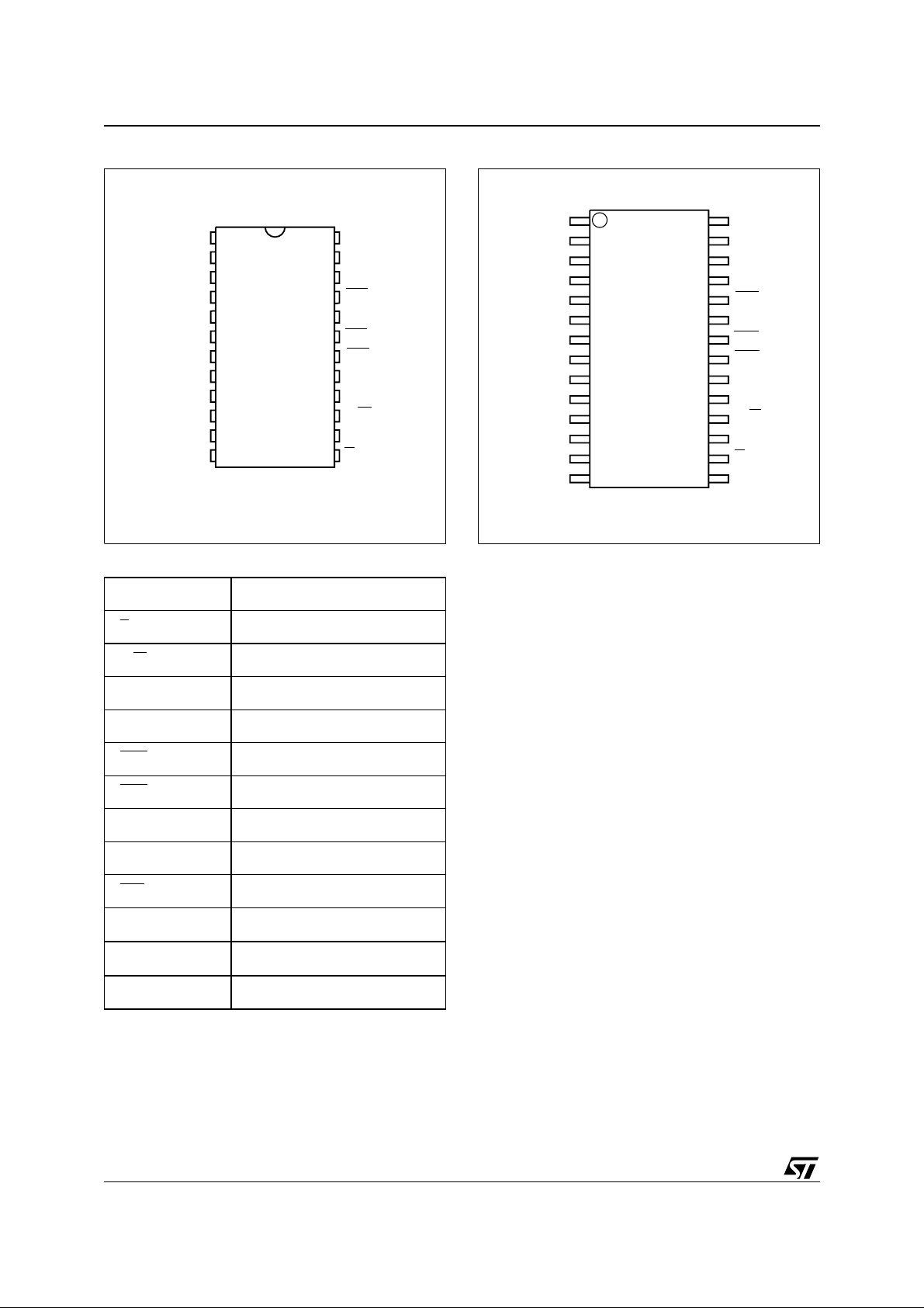
Figure 2. DIP C on ne ctions
MOT V
1
2
NC
3
NC
4
AD0
5
AD1
6
AD2
AD3
AD4
AD5
AD6
V
SS
M48T86
7
8
9
10
11
12 13
24
23
22
21
20
19
18
17
16
15
14
AI01641
CC
SQW
NC
RCL
NC
IRQ
RST
DS
NC
R/W
ASAD7
E
Table 1. Signal Names
AD0-AD7 Multiplexed Address/Data Bus
E
R/W
DS Data Strobe Input
AS Add ress Strob e Input
RST
RCL
MOT Bus Type Select Input
SQW Square Wave Output
IRQ
V
CC
V
SS
NC Not Connected Internally
Chip Enable Input
Write Enable Input
Reset Input
RAM Clear Input
Interrupt Request Output
Supply Voltage
Ground
Figure 3. SOIC Connections
1
MOT V
NC
NC
AD0
AD1
AD2
AD3
AD4
AD5
AD6
V
SS
V
SS
2
3
4
5
6
7
8
9
10
11
12
13
14
M48T86
28
27
26
25
24
23
22
21
20
19
18
17
16
15
AI01642
NCNC
CC
SQW
NC
RCL
NC
IRQ
RST
DS
NC
R/W
ASAD7
E
NC
DESCRIPTION
The M48T86 is an industry standard real time
clock (RTC).The M48T86 is composed of a lithium
energy source, quartz crystal, write-protection c ircuitry, and a 128 byte RAM array. This prov ides
the user with a complete subsystem packaged in
either a 24-pin DIP CAPHAT or 28-pin SNA PH AT
SOIC. Functions available to the user include a
non-volatile time-of-day clock, alarm interrupts, a
one-hundred-year clock with programmable in terrupts, square wave output, and 128 bytes of nonvolatile stat ic R AM .
The 24 pin 600mil DIP CAPHAT™ houses the
M48T86 silicon with a quartz crystal and a long life
lithium button cell in a single package.
The 28 pin 330mil SOIC provides sockets with
gold plated contacts at both ends for direct connection to a separate SNAPHAT housing cont aining the battery and crystal. The unique design
allows the SNAPHAT battery package to be
mounted on top of the SOIC package after the
completion of the surface mount process.
Insertion of the SNAPHAT housing after reflow
prevents potential battery and crystal damage due
to the high temperatures required for device surface-mounting. The SNAPHAT housing is keyed
to prevent reverse insertion.
The SOIC and battery packages are shipped separately in plastic anti-static tubes or in Tape & Reel
form.
2/23

M48T86
Table 2. Absolute Maximum Ratings
Symbol Parameter Value Unit
T
A
T
STG
(2)
T
SLD
V
IO
V
CC
P
D
Note: 1. Stresses greater than those listed under "Absolute Maximum Ratings" may cause permanent damage to the device. This is a stress
rating only and functional operation of the devi ce at these or any other condi t i ons above those indicated in the operational section
of this spec ification is not im plied. Exposure t o the abso lute max imum rat ing cond itions for extende d period s of tim e may affe ct
reliability.
2. Soldering temperature not to exceed 260°C for 10 seconds (total thermal budget not to exceed 150°C for longer than 30 seconds).
CAUTION: Negative undershoots below –0.3V are not allowed on any pin whil e i n the Batter y Back-up mode.
CAUTION: Do NOT wave solder SOIC to avoid damaging SNAPHAT sockets.
Ambient Operating Temperature 0 to 70 °C
Storage Temperature (VCC Off, Oscillator Off)
Lead Solder Temperature for 10 seconds 260 °C
Input or Output Voltages –0.3 to 7.0 V
Supply Voltage –0.3 to 7.0 V
Power Dissipation 1 W
For the 28 lead SOIC, the battery/crystal package
part number is "M4T28-BR12SH1".
Automatic deselection of the device provides insurance that data integrity is not compromised
should V
lect Voltage (V
fall below specified Power-fail Dese-
CC
) levels. The automatic deselec-
PFD
tion of the device remains in effect upon power up
for a period of 200ms (max) after V
V
, provided that the Real Time Clock is running
PFD
and the count down chain is not reset. This allows
sufficient time for V
to stabilize and gives the
CC
system clock a wa ke up p er i o d so th a t a valid system reset can be established.
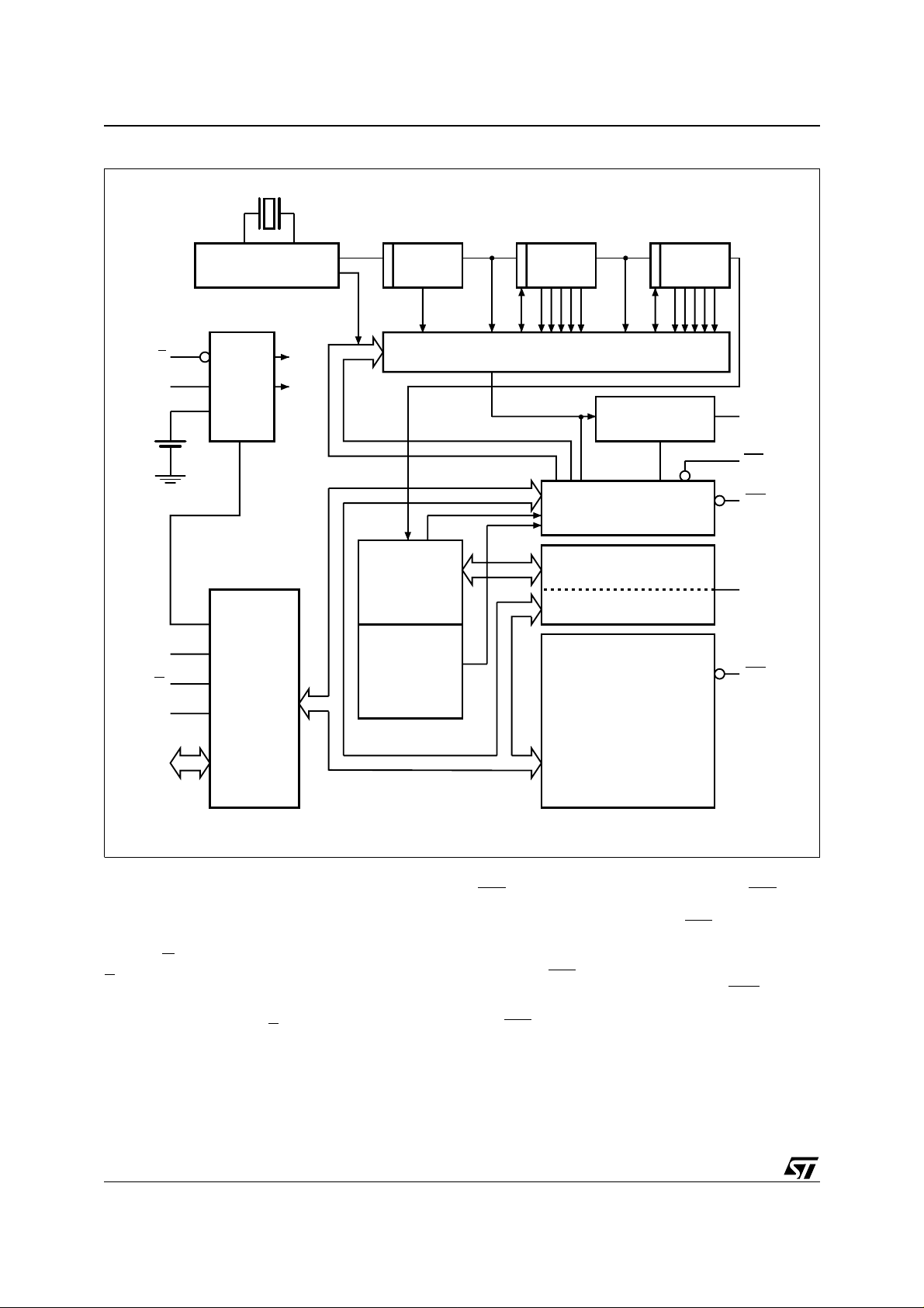
The block diagram in F igure 3 shows the pi n c onnections and the major internal functions of the
M48T86.
SIGNAL DESCRIPTION
V
, VSS. DC power is provided to the device on
CC
these pins.The M48T86 utilizes a 5V V
SQW (Square Wave Output). During n ormal op-
eration (i.e. valid V
), the SQW pin can output a
CC
signal from one of 13 taps.The frequenc y of the
SQW pin can be changed by programming Register A as shown in T able 10. Th e SQW signal can
be turned on and off using the SQWE bit (Register
B; bit 3). The SQW signal is not available when
V
is less than V
CC
PFD
.
(1)
rises above
CC
.
CC
–40 to 85 °C
AD0-AD7 (Multiplexed Bi-Directional Address/
Data Bus). The M48T86 provides a multiplexed
bus in which address an d data information s hare
the same signal path. The bus cycle consists of
two stages; first the address is latched, followed by
the data. Address/Data multiplexing does not slow
the access time of the M48T86, since the bus
change from address to data occurs during the internal RAM access time. Addresse s must be valid
prior to the falling edge of AS, at which time the
M48T86 latches the address present on AD0AD7. Valid write data must be present and held
stable during the latter port ion of the R/W
pulse. In
a read cycle, the M48T86 outputs 8 bits of data
during the latter portion of the DS pulse. The read
cycle is terminated and the bus returns to a high
impedance state upon a high transition on R/W
.
AS (Address Strobe Input). A positive going
pulse on the Address Strobe (AS) inp ut serves to
demultiplex the bus. The falling edge of AS causes
the address present on AD0-AD7 to be latched
within the M48T86.
MOT (Mode Select). The MOT pin offers the flexibility to choose between two bus types. When
connected to V
When connected to V
, Motorola bus timing is selected.
CC
or left disconnected, Intel
SS
bus timing is selected. The pin has an internal pulldown resistance of approximately 20K ohms.
3/23
M48T86
Figure 4. Block Diagram
V
V
BAT
R/W
CC
DS
AS
OSCILLATOR
E
POWER
SWITCH
AND
WRITE
PROTECT
BUS
INTERFACE
V
CC
POK
/ 8 / 64 / 64
PERIODIC INTERRUPT/SQUARE WAVE SELECTOR
REGISTERS A,B,C,D
CLOCK/
CALENDAR
UPDATE
BCD/BINARY
INCREMENT
CLOCK CALENDAR,
AND ALARM RAM
STORAGE
REGISTERS
(114 BYTES)
SQUARE WAVE
OUTPUT
SQW
IRQ
RST
DOUBLE
BUFFERED
RCL
AD0-AD7
DS (Data Strobe Input). The DS pin is also referred to as Read (RD). A falling edge transition on
the Data Strobe (DS) input enables the output during a a read cycle. This is very similar to an Output
Enable (G
(Chip Enable Input). The Chip Enable pin
E
) signal on other memory devices.
must be asserted low for a bus cycle in the
M48T86 to be accessed. Bus cycles which take
place without asserting E
will latch the addresses
present, but no data access will occur.
4/23
AI01643
IRQ (Inte rr upt R eq ue st Ou t put) . The IRQ pin is
an open drain output that can be used as an interrupt input to a processor. The IRQ
output remains
low as long as the status bi t causing the interrupt
is present and t he corresponding interrup t-enable
bit is set. IRQ
whenever Register C is read. The RST
returns to a hi gh impedance state
pin can
also be used to clear pending interrupts. Because
the IRQ
external pul l-up resis tor to V
bus is an open drain output, it requires an
.
CC

M48T86
RST (Reset Input). The M48T86 is reset when
the R ST
plied and a low on RST
input is p ulled lo w. With a valid VCC ap-
, the following event s oc-
cur:
1. Periodic Interrupt Enable (PIE) bit is cleared to
a zero. (Register B; Bit 6)
2. Alarm Interrupt Enable (AIE) b it is cleared to a
zero.(Register B; bit 5)
3. Update Ended Interrupt Request (UF) bit is
cleared to a zero. (Register C; Bit 4)
4. Interrupt Request (IRQF) bit is cleared to a zero.
(Register C Bit 7)
5. Periodic Interrupt Flag (PF) bit is cleared to a
zero. (Register C; Bit 6)
6. The device is not accessible until RST
is re-
turned high.
7. Alarm Interrupt Flag (AF) bit is cleared to a zero.
(Register C; Bit 5)
8. The IRQ
pin is in the high impedance state.
9. Square Wave Output Enable (SQWE) bit is
cleared to zero. (Register B; Bit 3).
10.Update Ended Interrupt Enable (UIE) is cleared
to a zero. (Register B; Bit 4)
RCL
(RAM Clear). The RCL pin is used to clear
all 114 storage bytes, excluding clock and control
registers, of the array to FF(hex ) value. T he array
will be cleared when the RCL
pin is held low for at
least 100ms with the osc illator running. Usage of
this pin does not affect battery load. This function
is applicable only when V
(Read/Write Input). The R/W pin i s utilized
R/W
is applied .
CC
to latch data into the M 48T86 and prov ides functionality si milar to W
in other memory systems.
ADDRESS MAP
The address map of the M48T86 is shown in Figure 9. It consists of 114 bytes of user RAM, 10
bytes of RAM that contain the RTC time, calendar
and alarm data, and 4 bytes which are used for
control and status. All bytes can be read or written
to except for the following:
1. Registers C & D are read-only.
2. Bit 7 of Register A is read-only.
The contents of the four Registers A, B, C, and D
are described in the "Registers" section.
5/23

M48T86
Table 3. Time, Calendar and Alarm Formats
Address RTC Bytes
Decimal Binary BCD
0 Seconds 0-59 00-3B 00-59
1 Seconds Alarm 0-59 00-3B 00-59
2 Minutes 0-59 00-3B 00-59
3 Minutes Alarm 0-59 00-3B 00-59
Hours, 12-hrs 1-12
4
Hours, 24-hrs 0-23 00- 17 00-23
Hours Alarm, 12-hrs 1-12
5
Hours Alarm, 24-hrs 0-23 00-17 00-23
6 Day of Week (1 = Sun) 1-7 01-07 01-07
7 Day of Month 1-31 01-1F 01-31
8 Month 1-12 01-0C 01-12
9 Year 0-99 00-63 00-99
Range
01-0C AM
81-8C PM
01-0C AM
81-8C PM
01-12 AM
81-92 PM
01-12 AM
81-92 PM
TIME, CALENDAR, AND ALARM LOCATIONS
The time and calendar information is obtained by
reading the appropriate memory bytes. Th e time,
calendar, and alarm registers are set o r initialized
by writing the appropriate RAM bytes. The contents of the time, calendar, and alarm bytes can be
either Binary or Binary-Coded Decimal (BCD) format. Before writing the internal time, calendar, and
alarm register, the SET bit (Register B; Bit 7)
should be written to a logic "1". This will prev ent
updates from occurring while access is being attempted. In addition to writing the time, calendar,
and alarm registers in a selected format (binary or
BCD), the Data Mode (DM) bit (Register B ; Bit 2),
must be set to the appropriate logic level ("1" signifies binary data; "0" signifies Binary Coded Decimal (BCD data). All time, calendar, and alarm
bytes must use the same data mode. The SET bit
should be cleared after the Data Mode bit has
been written to allow the Real Time Clock to update the time and calendar bytes. Once initialized,
the Real Time Clock makes all updates in the selected mode. The da ta mode cann ot be changed
without reinitializing the ten data bytes. Table 3
shows the binary and BCD formats of the time, calendar, and alarm loc ations. The 24/ 12 bit (Register B; Bit 1) cannot be changed without
reinitializing the hour locations. When the 12-hour
format is selected, a logic one in the high order bit
of the hours byte represents PM. The time, calendar, and alarm bytes are always accessible because they are double buffered. Once per second
the ten bytes are advanced by one second and
checked for an alarm condition. If a read of the
time and calendar data occurs during an update, a
problem exists where seconds, minutes, hours,
etc. may not correlate. However, the probability of
reading incorrect time and calendar data is low.
Methods of avoiding possible incorrect time and
calendar reads are reviewed later in this text.
NON-VOLATILE RAM
The 114 general purpose non-volatile RAM bytes
are not dedicated to any special function within the
M48T86. They can be used by t he proces sor program as non-volatile me mory a nd a re f ully a ccessible during the update cycle.
6/23
M48T86
Figure 5. AC Testing Load Circuit
5V
FOR ALL
OUTPUTS
EXCEPT IRQ
510Ω
960Ω
50pF
AI01644
Figure 6. AC Testing Load Circuit
IRQ
Table 4. AC Measurement Conditions
Input Rise and Fall Times ≤ 5ns
Input Pulse Voltages 0 to 3V
Input and Output Timing Ref. Voltages 1.5V
Note that Output Hi-Z is defined as the point where data is no longer driven.
5V
1.15kΩ
130pF
AI01645
Table 5. Capacitance
= 25 °C, f = 1 MHz)
(T
A
(1, 2)
Symbol Parameter Test Condition Min Max Unit
V
V
OUT
IN
= 0V
= 0V
7pF
5pF
C
IN
C
IO
Note: 1. Effective capacitance measured with power supply at 5V .
2. Sampled only, not 100% tested.
3. Outputs desele ct ed.
Input Capacitance
(3)
Input / Output Capacitance
Table 6. DC Characteristics (1)
= 0 to 70 °C; VCC = 4.5V to 5.5V)
(T
A
Symbol Parameter Test Condition Min Max Unit
(1)
Input Leakage Current
I
LI
(1)
I
LO
I
CC
V
V
Output Leakage Current
Supply Current Outputs open 15 mA
Input Low Voltage –0.3 0.8 V
IL
Input High Voltage 2.2
IH
Output Low Voltage
V
OL
Output Low Voltage (IRQ
V
OH
Note: 1. Outputs deselected .
Output High Voltage
)
0V ≤ V
0V ≤ V
I
OL
I
OL
I
OH
≤ V
IN
≤ V
OUT
= 4mA
= 0.5mA
= –1mA
CC
CC
±1 µA
±1 µA
V
+ 0.3
CC
0.4 V
0.4 V
2.4 V
V
7/23

M48T86
Table 7. Power Down/Up Trip Points DC Characteristics
(1)
(TA = 0 to 70 °C)
Symbol Parameter Min Typ M ax Uni t
V
PFD
V
SO
t
DR
Note: 1. All voltages referenced to VSS.
2. At 25°C.
Power-fail Deselect Voltage 4.0 4.35 V
Battery Back-up Switchover Voltage 3.0 V
(2)
Expected Data Retention Time 10 YEARS
Table 8. Power Down/Up Mode AC Characteristics
(TA = 0 to 70°C)
Symbol Parameter Min Max Unit
(1)
t
F
t
R
t
REC
Note: 1. VCC fall time of less than tF may result in deselection/write protection not occurring until 200µs after VCC passes V
VCC Fall Time
VCC Rise Time
V
to E High
PFD
300 µs
100 µs
20 200 ms
PFD
Figure 7. Power Down/Up Mode AC Waveforms
.
V
CC
4.5V
V
PFD
VSO
tF tR
E
INTERRUPTS
The RTC plus RAM includes three separate, fully
automatic sources of interrupt (alarm, periodic, update-in-progress) available to a processor. The
alarm interrupt can be programmed to occur at
rates from once per second t o onc e per day. The
periodic interrupt can be selected from rates of
500ms to 122µs. The update-end ed interrupt can
be used to indicate that an update cycle has completed.
The processor program can select which interrupts, if any, are going to be used. Th ree bits in
tREC
AI01646
Register B enable the interrupts. Writing a logic "1"
to an interrupt-enable bit (Register B; Bit 6 = PIE;
Bit 5 = A IE; B it 4 = UIE) permits an interrupt to be
initialized when the event occurs. A zero in an interrupt-enable bit prohibits the IRQ
pin from being
asserted from that in terrupt condition. If an interrupt flag is already set when an interrupt is enabled, IRQ
is immediately set at an active level,
although the interrupt initiating the event may have
occurred much earlier. As a result, there are cases
where the program should clear such earlier initiated interrupts before first enabling new interrupts.
8/23

Table 9. AC Characteristics
(T
= 0 to 70 °C; VCC = 4.5V to 5.5V)
A
Symbol Parameter
t
CYC
t
DSL
t
DSH
t
RWH
t
RWS
t
CS
t
CH
t
DHR
t
DHW
t
AS
t
AH
t
DAS
t
ASW
t
ASD
t
OD
t
DW
t
BUC
(1)
t
PI
t
UC
Note: 1. See Tabl e 10.
Cycle Time 160 ns
Pulse Width, Data Strobe Low or R/W High 80 ns
Pulse Width, Data Strobe High or R/W Low 55 ns
R/W Hold Time 0 ns
R/W Setup Time 10 ns
Chip Select Setup Time 5 ns
Chip Select Hold Time 0 ns
Read Data Hold Time 0 25 ns
Write Data Hold Time 0 ns
Address Setup Time 20 ns
Address Hold Time 5 ns
Delay Time, Data Strobe to Address Strobe Rise 10 ns
Pulse Width Address Strobe High 30 ns
Delay Time, Address Strobe to Data Strobe Rise 35 ns
Output Data Delay Time from Data Strobe Rise 50 ns
Write Setup Time 30 ns
Delay Time before Update Cycle 244 µs
Periodic Interrupt Time interval – – –
Time of Update Cycle 1 µs
M48T86
M48T86
Unit
Min Typ Max
When an interrupt event occurs, the related flag bit
(Register C; Bit 6 = PF; Bit 5 = AF; Bit 4 = UF) is
set to a logic "1". These flag bits are set independent of the state of the corresponding enable bit in
Register B and can be used in a polling mode without enabling the corresponding enable b its. The
interrupt flag bits are status bits which software
can interrogate as necessary.
When a flag is set, an in dication is given to software that an interrupt event has occurred since the
flag bit was last read; however, care should be taken when using the flag bits as all are cleared each
time Register C is read. Doubl e la tching is i ncluded with Register C so that bits which are set, remain stable throughout the read cycle. All bits
which are set high are cleared when read. Any
new interrupts which are pendi ng during the read
cycle are held until after the cycle is completed.
One, two, or three bits can be s et when reading
Register C. Each utilized flag b it should be examined when read to ensure that no interrupts are
lost.
The second flag bit usage meth od is with fully enabled interrupts. When an interrupt flag bit is set
and the corresponding enable bit is also set, the
IRQ
pin is asserted low. IRQ is asserted as long as
at least one of the three interrupt sources has i ts
flag and enable bits both set. The IRQF bit (Register C; Bit 7) is a "1" whenever the IRQ
pin is being
driven low. Determination that the RTC initiated an
interrupt is accomplished by reading Register C.A
logic "1" in the IRQF bit indicates that one or more
interrupts have been initiated by the M48T86. The
act of reading Register C clears all active flag bits
and the IRQF bit.
9/23

M48T86
Figure 8. Intel Bus Read Mode AC Waveforms
AS
DS
tDSL tDSH
R/W
tDAS tCS tOD tCH
E
tAS tAH tDHR
AD0-AD7
tCYC
tASDtASW
AI01647
Figure 9. Intel Bus Write AC Waveforms
AS
tDAS
DS
R/W
E
AD0-AD7
tCYC
tASDtASW
tDSL tDSH
tCS
tAS tAH
tDW
tCH
tDHW
AI01648
10/23

Figure 10. Motorola Bus Read/Write Mode AC Waveforms
AS
M48T86
DS
R/W
E
AD0-AD7
(Write)
AD0-AD7
(Read)
tDAS
tASDtASW
tCYC
tDSL
tRWS
tCS
tAH
tAS tDHW
tAS tOD
tAH
tDSH
tRWH
tCH
tDW
tDHR
AI01649
PERIODIC INTERRUPT
The periodic interrupt will cause the IRQ
pin to go
to an active state from once every 500ms to once
every 122µs. This function is separate from the
alarm interrupt which can be output from once per
second to once per day. The periodic interrupt rate
is selected using the same Register A bits which
select the square wave frequency (see T able 10 ).
Changing the Register A bits affects both the
square wave frequency and the periodic interrupt
output. However, each function has a separate enable bit in Register B. The periodic interrupt is enabled by the PIE bit (Register B; Bit 6). The
periodic interrupt can be used with software
counters to measure inputs, create output intervals, or await the next needed software function.
ALARM INTERRUPT
The alarm interrupt provides the system processor
with an interrupt when a match is made between
the RTC's hours, minutes, and seconds bytes and
the corresponding alarm bytes.
The three alarm bytes can be used in two way s.
First, when the alarm time is written in the appropriate hours, minutes, and seconds alarm locations, the alarm interrupt is initiated at the specified
time each day if the Alarm Interrupt Enable bit
(Register B; Bit 5) is high. The second use is to insert a "don't care" state in one or more of the three
alarm bytes. The "don't care" code is any hexadecimal value from C0 to FF. The two most significant
bits of each byte set the "don't care" condition
when at logic "1". An alarm will be generated each
hour when the "don't care" is are set in the hours
byte. Similarly, an alarm is generated every minute
with "don't care" codes in the hour and minute
alarm bytes. The "don't care" codes in all three
alarm bytes create an interrupt every second.
11/23

M48T86
Figure 11. Address Map
00
0D
0E
7F
14
BYTES
114
BYTES
0
CLOCK AND CONTROL
STATUS REGISTERS
13
14
STORAGE REGISTERS
127
UPDATE CYCLE INTERRUPT
After each update cycle, the updat e cycle ended
flag bit (UF) (Register C; Bit 4) is set to a "1". If the
update interrupt enable bit (UIE) (Register B; Bit 4)
is set to a "1", and the SET bit (Register B; Bit 7) is
a "0", then an interrupt request is generated at the
end of each update cycle.
SQUARE WAVE OUTPUT SELECTION
Thirteen of the 15 divider taps are made available
to a 1-of-15 selector, as sho wn in the block diagram of Figure 3. The purpose of selecting a divider tap is to generate a squa re wave ou tput signal
on the SQW pin. The RS3-RS0 bits in Reg ister A
establish the square wave output frequency.
These frequencies are listed in Table 10. The
0
1
2
3
4
5
6
7
8
9
10
11
12
13
SECONDS
SECONDS ALARM
MINUTES
MINUTES ALARM
HOURS
HOURS ALARM
DAY OF WEEK
DATE OF MONTH
MONTH
YEAR
REGISTER A
REGISTER B
REGISTER C
REGISTER D
BCD OR
BINARY
FORMAT
AI01650
SQW frequency selection sha res the 1-of-15 selector with the periodic interrupt generator. Once
the frequency is selected, the output of the SQW
pin can be turned on and off under program control
with the square wave enabled (SQWE).
OSCILLATOR CONTROL BITS
When the M48T86 is ship ped from the f ac tory the
internal oscillator is turned off. This feature prevents the lithium energy cell from being discharged until it is installed in a system. A pattern of
"010" in Bits 4-6 of Register A will turn the oscillator on and enable the countdown chain. A p attern
of "11X" will turn the oscillator on, but holds the
countdown chain of the oscillator in reset. All other
combinations of Bits 4-6 keep the oscillator off.
12/23

Table 10. Square Wave Frequen cy/P eriodi c Interru pt R ate
Register A Bits Square Wave Periodic Interrupt
RS3 RS2 RS1 RS0 Frequency Units Period Units
0000None None
0001256Hz3.90625 ms
0010128Hz7.8125 ms
00118.192 kHz 122.070 us
01004.096 kHz 244.141 us
01012.048 kHz 488.281 us
01101.024 kHz 976.5625 us
0111512Hz1.953125 ms
1000256Hz3.90625 ms
1001128Hz7.8125 ms
101064Hz15.625 ms
101132Hz31.25 ms
110016Hz62.5 ms
M48T86
11018Hz125ms
11104Hz250ms
11112Hz500ms
UPDATE CYCLE
The M48T86 executes an up date cycle once per
second regardless of the SET bit (Register B; Bit
7). When the SET bit is asserted, the user copy of
the double buffered time, calendar, and alarm
bytes is frozen and will not update as the time increments. However, the time countdown chain
continues to update the internal copy of the buffer.
This feature allows accurate time to be maintained, independent of reading and writing the
time, calendar, and alarm buffers. This also guarantees that the time and calendar informat ion will
be consistent. The update cycle also compares
each alarm byte with the corresponding time byte
and issues an alarm if a match or if a "don't care"
code is present in all three positions.
There are three methods of accessing the real
time cloc k that wil l avoi d an y pos sib ility of ob taining inconsistent time and calendar data. The first
method uses the update-ended interrupt. If enabled, an interrupt occurs after every update cycle
which indicates that over 999ms are available to
read valid time and date information. If this interrupt is used, the IRQF bit (Register C; Bit 7) should
be cleared before leaving the interrupt routine.
A second method uses the Update-In-Progress
(UIP) bit (Register A; Bit 7) to determine if the update cycle is in progress. The UIP bit will pulse
once per second. Afte r the UIP bi t goes h igh, the
update transfer occurs 244µs later. If a low is read
on the UIP bit, the user has at least 244µs before
the time/calendar data will be changed. Therefore,
the user should avoid interrupt service routines
that would cause the time needed to read valid
time/calendar data to exceed 244µs.
The third method uses a periodic interrupt to determine if an update cycle is in progress. The UIP bit
is set high between the setting of the PF bit (Register C; Bit 6). Periodic interrupts that occur at a
rate greater than t
allow valid time and date in-
BUC
formation to be reached at each occurrence of the
periodic interrupt.The reads should be completed
within 1/(t
PL/2
+ t
) to ensure t hat data is not
BUC
read during the update cycle.
13/23

M48T86
Figure 12. Upd at e Period Timing and UIP
UPDATE PERIOD (1sec)
UIP
Figure 13. Update-ended/Periodic Interrupt Relationship
UPDATE PERIOD (1sec)
tBUC tUC
AI01651
UIP
PF
UF
tPI
tPI tPI
tBUC tUC
AI01652B
14/23

REGISTER A
MSB
BIT7 BIT6 BIT5 BIT4 BIT3 BIT2 BIT1 BIT0
UIP OSC2 OSC1 OSC0 RS3 RS2 RS1 RS0
M48T86
UIP. Update in Progress
The Update in Progress (UIP) b it is a status flag
that can be monitored. When the UIP bit is one,
the update transfer will soon occur. When UIP isa
zero, the update transfe r will not occur for at least
244µs. The time, calendar, and alarm inform ation
in RAM is fully availa ble f or a ccess whe n the UIP
bit is zero. The UIP bit is read only and is not affected by RST. Writing the SET bit in Register B to
a "1" inhibits any update transfer and clears the
UIP status bit.
OSC0, OSC1, OSC2. Oscillator Control
These th ree b its a re used to cont rol t he osc illator
and reset the countdown chain. A pattern of "010"
enables operation by turning on the oscillator and
enabling the divider chain. A pattern of 11X turns
the oscillator on, but keeps the frequency d ivider
disabled. When "010" is written, the first update
begins after 500ms.
RS3, RS2, RS1, RS0
These four rate-selection bits select one of the 13
taps on the 15-stage divider or disable the divider
output. The tap selected may be used to generate
an output square wave (SQW pin) and/or a periodic interrupt. The user may do one of the following:
1. Enable the interrupt with the PIE bit;
or
2. Enable the SQW output with the SQWE bit;
or
3. Enable both at the same time and same rate;
or
4. Enable neither.
Table 10 lists the peri odic interrupt rates and the
square wave frequencies that may be chosen with
the RS bits. These four read/write bits a re not a ffected by RST.
15/23

M48T86
REGISTER B
MSB
BIT7 BIT6 BIT5 BIT4 BIT3 BIT2 BIT1 BIT0
SET PIE AIE UIE SQWE DM 24/12 DSE
SET
When the SET bit is a zero, the update transfer
functions normally by advancing the counts once
per second. When the SET bit is written to a one,
any update transfer is inhibited and t he program
may initialize the time and calenda r bytes without
an update occurring. Read cycles can be executed
in a similar manner. SET is a read/write bit which
is not modified by RST
or internal functions of the
M48T86.
PIE. Period ic Int errupt Enable
The Periodic Interrupt Enable bit (PIE) is a read/
write bit which allows the Periodic Interrupt Flag
(PF) bit Register C to cause the IRQ
pin to be driven low. When the PIE bit is set to one, periodic interrupts are generated by driving the IRQ
pin low
at a rate specified by the RS3-RS0 bits of Register
A. A zero i n the PIE bit blocks the I RQ
output from
being driven by a periodic interrupt, but the Periodic Flag (PF) bit is still set at the periodic rate. P IE
is not modified by any internal M 48T86 func tions,
but is cleared to zero on RST
.
AIE. Alarm Interrupt Enable
The Alarm Interrupt Enable (AIE) bit is a Read/
Write bit which, when set to a one, permits the
Alarm Flag (AF) bit in Register C to assert IRQ
. An
alarm interrupt occurs for each second that the
three time bytes equal the three alarm bytes including a "don’t care" alarm code of binary
1XXXXXXX. When the AIE bit is set to zero, the
AF bit does not initiate the IRQ
signal. The RST
pin clears AIE to zero. The internal functions of the
M48T86 do not affect the AIE bit.
UIE. Update E nd e d In terrupt Enable
The Update Ended Interrupt Enable (UIE) bit is a
read/write bit which enables the Update End Flag
(UF) bit in Register C to assert IRQ
low on the RST
pin or the SET bit going high clears
. A transition
the UIE bit.
SQWE. Square Wave Enable
When the Square Wave Enable (SQW E) bit is set
to a one, a square wave signal is driven out on the
SQW pin. The frequency is determined by the
rate-selection bits RS3-RS0. W hen th e S QW E bit
is set to zero, the SQW pin is held low. The SQWE
bit is cleared by the RST
pin. SQWE is a read/write
bit.
DM. Data Mode
The Data Mode (DM) bit indicates whether time
and calendar information are in binary or BCD format. The DM bit is set by the program to the appropriate format and can be read as required. This bit
is not modified by internal function or RST
. A one
in DM signifies binary data and a zero specifies Binary Coded Decimal (BCD) data.
24/12
The 24/12 control bit establishes the format of the
hours byte.A one indicates the 24-hour m ode and
a zero indicates the 12-hour mode. This bit is read/
write and is not affected by i nternal functions or
RST
.
DSE. Daylight Savings Enable
The Daylight Savings Enable (DSE) bit is a read/
write bit which enables two special updates when
set to a one. On the f irst Sunday i n A pril, the t ime
increments from 1:59:59AM to 3:00:00 AM. On the
last Sunday in October, when the time reaches
1:59:59 AM, it changes to 1:00:00 AM. These special updates do not occur when the DSE bit is a zero. This bit is not affected by internal functions or
.
RST
16/23

M48T86
REGISTER C
MSB
BIT7 BIT6 BIT5 BIT4 BIT3 BIT2 BIT1 BIT0
IRQFPFAFUF0000
IRQF. Interrupt Request Flag
The Interrupt Request Flag (IRQ F) bit is set to a
one when one or more of the following are true:
PF = PIE = 1
AF = AIE = 1
UF = UIE = 1
(i.e. IRQF = PF*PIE+A F*AIE+UF*UI E )
PF. Periodic I nte rru pt Fl ag
The Periodic Interrupt Flag (PF) is a read -only bit
which is set to a one when an edge is detected on
the selected tap of the divider chain. The RS3-RS0
bits establish the periodic rate. PF is set to a one
independent of the state of the PIE bit. The I RQ
signal is active and will set the IRQF bit. The PF bit
is cleared by a RST
or a software read of Register
AF. Alarm Flag
A one in the AF (Alarm Interrupt F lag) bit i ndicates
that the current time has m at ched the alarm time.
If the AIE bit is also a one, the IRQ
pin will go low
and a one will ap pear i n the IRQF bit. A RST
read of Register C will clear AF.
UF. Update Ended Interrupt Fl ag
The Update Ended Interrupt Flag (UF) bit is set after each update cycle. When the UIE bit is set to a
one, the one in the UF bit causes the IRQF bit to
be a one. This will assert the IRQ
cleared by reading Register C or an RST
pin. UF is
.
BIT 0 through 3 . Un used Bits
Bit 3-Bit 0 are unused. These bits always read
zero and cannot be written.
C.
REGISTER D
MSB
BIT7 BIT6 BIT5 BIT4 BIT3 BIT2 BIT1 BIT0
VRT0000000
or a
VRT. Valid Ram And Time
The Valid RAM and Tim e (VRT) bit is set to the
one state by STMicroelectronics prior to shipment.
This bit is not writable and should always be a one
when read. If a zero is ever present, an exhausted
internal lithium cell is indicated and both the contents of the RTC data and RAM data are questionable. This bit is unaffected by RST
.
BIT 0 through 6 . Un used Bits
The remaining bits of Register D are not usable.
They cannot be written and when read, they will always read zero.
17/23

M48T86
POWER SUPPLY DECOUPLING
and UNDERSHOOT PROTECTION
I
transients, including those produced by output
CC
switching, can produce voltage fluctuations, resulting in spikes on the V
bus. These transients
CC
can be reduced if capacitors are used to store energy, which stabilizes the V
bus. The energy
CC
stored in the bypass capacitors will be released as
low going spikes are generated or energy will be
absorbed when overshoots occur. A ceramic by-
pass capacitor value of 0.1µF (as shown in Figure
14) is recommended in order to provide the needed filtering.
In addition to transients that are caused by normal
SRAM operation, power cycling can generate negative voltage spikes on VCC that drive it to values
below V
by as much as one Volt. These nega-
SS
tive spikes can cause data corruption in the SRAM
while in battery backup mode. To protect from
these voltage spikes, it is recommended to connect a schottky diode from V
connected to V
, anode to VSS). Schottky diode
CC
to VSS (cathode
CC
1N5817 is recommended for through hole and
MBRS120T3 is recommended for surface mount.
Figure 14. Supply Voltage Protection
V
CC
V
CC
0.1µF DEVICE
V
SS
AI02169
18/23

Table 11. Ordering Information Scheme
Example: M48T86 MH 1 TR
Device Type
M48T
Package
PC = PCDIP24
(1)
MH
= SOH28
Temperature Range
1 = 0 to 70 °C
Shipping Method for SOIC
blank = Tubes
TR = Tape & Reel
M48T86
Note: 1. The SOIC package (SOH28) requires the battery/crystal package (SNAPHAT) which is ordered separately under the part number
"M4T28-BR12SH1" in pl astic tube or " M 4T28-BR12SH1TR" in T ape & Reel for m.
Caution: Do not place the SNAPHAT battery/crystal package "M 4T28-BR12SH1" in conduct ive foam since will drain the li thium button-cell
battery.
For a list of available options (Speed, Pac kage, etc...) or for furthe r information on any aspect of this device, please contact the ST Sales Office nearest to you.
Table 12. Revision History
Date Revision Details
March 1999 F irst Issue
05/04/00 Page layout changed
19/23

M48T86
Table 13. PCDIP24 - 24 pin Plastic DIP, battery CAPHAT, Package Mechanical Data
Symb
Typ Min Max Typ Min Max
A 8.89 9.65 0.3500 0.3799
A1 0.38 0.76 0.0150 0.0299
A2 8.36 8.89 0.3291 0.3500
B 0.38 053 0.0150 0 .0209
B1 1.14 1.78 0.0449 0.0701
C 0.20 0.31 0.0079 0.0122
D 34.29 34.80 1.3500 1.3701
E 17.83 18.3 4 0.7020 0.7220
e1 2.29 2.79 0.0 902 0.1098
e3 25.15 30.7 3 0.9902 1.2098
eA 15.24 16.00 0.6000 0.6299
L 3.05 3.81 0.1 201 0.1500
N24 24
mm inches
Figure 15. PCDIP28 - 28 pin Plastic DIP, battery CAPHAT, Package Outline
A2
A1AL
B1 B e1
eA
e3
D
N
E
1
Drawing is not to scale.
C
PCDIP
20/23

M48T86
Table 14. SOH28 - 28 lead Plastic Small Outline, 4-socket battery SNAPHAT, Package Mechanical Data
Symb
Typ Min Max Typ Min Max
A 3.05 0.1201
A1 0.05 0.36 0.0020 0.0142
A2 2.34 2.69 0.0921 0.1059
B 0.36 0.51 0.0142 0.0201
C 0.15 0.32 0.0059 0.0126
D 17.71 18.49 0.6972 0.7280
E 8.23 8.89 0.3240 0.3500
e 1.27 – – 0.0500 – –
eB 3.20 3.61 0.1260 0.1421
H 11.51 12.70 0.4531 0.5000
L 0.41 1.27 0.0161 0.0500
α 0° 8° 0° 8°
N 28 28
mm inches
CP 0.10 0.0039
Figure 16. SOH28 - 28 lead Plastic Small Outline, 4-socket battery SNAPHAT, Package Outline
A2
A
C
Be
eB
CP
D
N
E
H
LA1 α
1
SOH-A
Drawing is not to scale.
21/23

M48T86
Table 15. M4T28-BR12SH - SNAPHAT Housing for 48 mAh Battery & Crystal, Package Mechanical Data
Symb
Typ Min Max Typ Min Max
A 9.78 0.3850
A1 6.73 7.24 0.2650 0.2850
A2 6.48 6.99 0.2551 0.2752
A3 0.38 0.0150
B 0.46 0.56 0.0181 0.0220
D 21.21 21.84 0.8350 0.8598
E 14.22 14.99 0.5598 0.5902
eA 15.55 15.95 0.6122 0.6280
eB 3.20 3.61 0.1260 0.1421
L 2.03 2.29 0.0799 0.0902
mm inches
Figure 17. M4T28-BR12SH - SNAPHAT Housing for 48 mAh Battery & Crystal, Package Outline
A2
A3
L
eA
D
A1
A
B
eB
E
SH
Drawing is not to scale.
22/23

M48T86
Information furnished is believed to be ac curate and reliable. Howev er, STMicroelectronics assumes no resp onsibility for t he consequ ences
of use of such information nor for any infringement of patents or other rights of third parties which may result from its use. No license is granted
by implic ation or oth erwise under any patent or pat ent rights of STMicroelectron i cs . Specifications mentioned in th i s publicati on are s ubject
to change without notice. This publication supersedes and replaces all information previously supplied. STMicroelectronics products are not
authorized for use as critical comp onents in life support devi ces or systems wi thout express written approval of STM i croelect ronics.
The ST log o i s registered trademark of STMicroelectronics
© 2000 STMicroelectronics - All Rights Reserved
All other names are the property of their respective owner s.
Australi a - Brazil - Chi na - Finland - F rance - Germ any - Hong Kon g - India - Italy - Japan - Malaysi a - Malta - Morocco -
Singapor e - Spain - Swede n - Switzerland - United Kingdom - U.S.A.
STMicroelect ro n ics GRO UP OF COMPANI ES
http://www.st.com
23/23
 Loading...