

SGS Thomson Microelectronics M40Z111W, M40Z111VMH1, M40Z111MH1, M40Z111 Datasheet
M40Z111
M40Z111W
NVRAM CO NTROLLER for up to TWO LPSRAM
February 1999 1/12
CONVERT LOW POWE R SRAMs into
NVRAMs
PRECISION POWER MONITORING and
POWER SWITCHING CIRCUITRY
AUTOMATIC WRITE-PROTECTION when V
CC
is OUT-OF-TOLERANCE
CHOICE of SUPPLY VOL TAGES and
POWER-FAIL DESELECT VOLTAGES:
– M40Z111:
V
CC
= 4.5V to 5.5V
THS = V
SS
4.5V ≤ V
PFD
≤ 4.75V
THS = V
OUT
4.2V ≤ V
PFD
≤ 4.5V
– M40Z111W:
V
CC
= 3.0V to 3.6V
THS = V
SS
2.8V ≤ V
PFD
≤ 3.0V
V
CC
= 2.7V to 3.3V
THS = V
OUT
2.5 ≤ V
PFD
≤ 2.7V
LESS THAN 15ns CHIP E NAB LE AC CESS
PROPAGATION DELAY (for 5.0V device)
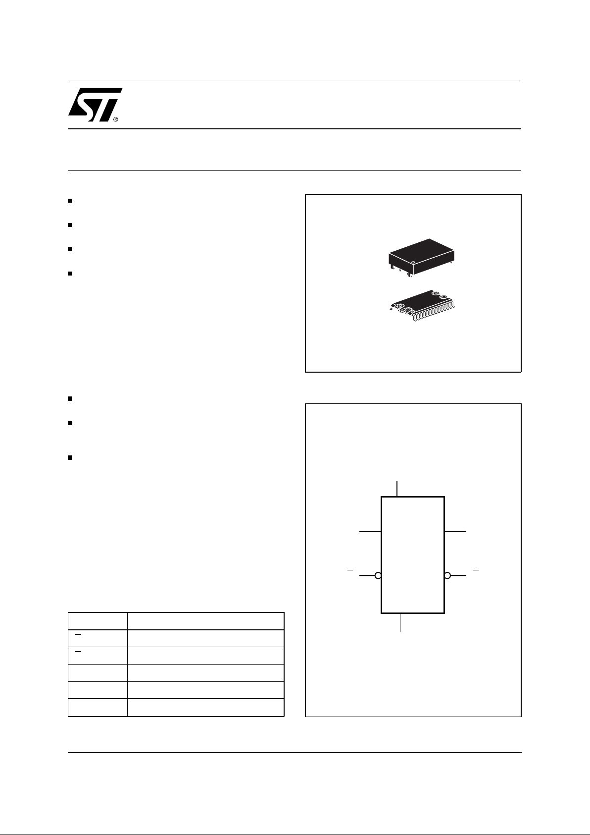
PACKAGING INCLUDES a 28-LEAD SOIC
and SNAPHAT
®
TOP
(to be Ordered Separately)
SOIC PACKAGE PROVIDES DIRECT
CONNECTION for a SNAPHAT TOP which
CONTAINS the BATTERY
DESCRIPTION
The M40Z111/111W NVRAM Controller is a selfcontained device which converts a standard lowpower SRAM into a non-volatile memory.
A precision voltage reference and comparator
monitors the V
CC
input for an out-of-tolerance con-
dition.
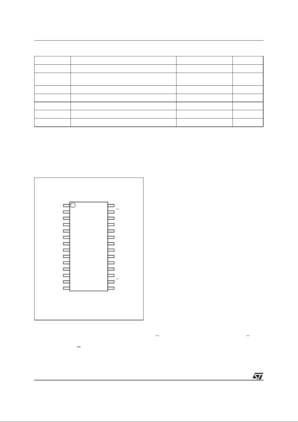
AI02238B
THS
V
CC
M40Z111
M40Z111W
E
CON
V
SS
E
V
OUT
Figure 1. Logic Diagram
THS Threshold Select Input
E Chip Enable Input
E
CON
Conditioned Chip Enable Output
V
OUT
Supply Voltage Output
V
CC
Supply Voltage
V
SS
Ground
Table 1. Signal Names
SNAPHAT (SH)
Battery
28
1
SOH28 (MH)
AI02239B
8
2
3
4
5
6
7
9
10
11
12
13
14
22
21
20
19
18
17
16
15
28
27
26
25
24
23
1
NC
NC
NC
NC
V
CC
NC
V
CC
NC
NC
NC
NC
NC
NC
NC
E
NC
NC
NC
NCNC
THS
NCV
SS
E
CON
NC
NC
V
OUT
V
CC
M40Z111
M40Z111W
Figure 2. SOIC Pin Connections
Warning:
NC = Not Connected.
Symbol Parameter Value Unit
T
A
Ambient Operating Temperature 0 to 70 °C
T
STG
Storage T emper ature (VCC Off) SNAPHAT
SOIC
–40 to 85
–55 to 125
°C
T
SLD
(2)
Lead Solder Temperature for 10 seconds 260 °C
V
IO
Input or Output Voltages –0.3 to VCC +0.3 V
V
CC
Supply Voltage –0.3 to 7 V
I
O
Output Current 20 mA
P
D
Power Dissipation 1 W
Notes:
1. Stresses greater than those listed under "Absolute Maximum Ratings" may cause permanent damage to the device. This is a
stress rating only and functional operation of the device at these or any other conditions above those indi cat ed in the operati onal
section of this specification is not implied. Exposure to the absolute maximum rating conditions for extended periods of time may
affect reliability.
2. Soldering temperature not to exceed 260°C for 10 seconds (total thermal budget not to exceed 150°C for longer than 30 seconds).
CAUTION: Negat i ve undershoots below –0.3 volts are not allowed on any pin while in the Battery Back-up mode.
CAUTION: Do NOT wave solder SOIC to avoid damaging SNAPHAT sockets.
T ab le 2. Absolute Maximum Ratings
(1)
When an invalid VCC condition occurs, the conditioned chip enable (
E
CON
) output is forced inactive
to write-protect the stored data in the SRAM.
During a power failure, the SRAM is switched from
the V
CC
pin to the lithium cell within the SNAPHAT
to provide the energy required for data retention.
On a subsequent power-up, the SRAM remains
write protected until a valid power condition returns.
The 28 pin 330mil SOIC provides sockets with gold
plated contacts at both ends for direct connection
to a separate SNAPHAT housing containing the
battery. The unique design allows the SNAPHAT
battery package to be mounted on top of the SOIC
package after the completion of the surface mount
process. Insertion of the SNAPHAT housing after
reflow prevents potential battery damage due to the
high temperatures required for device surfacemounting. The SNAPHAT housing is keyed t o prevent reverse insertion. The SOIC and battery
packages are shipped separately in plastic antistatic tubes or in Tape & Reel form. For the 28 lead
SOIC, the battery package (i.e. SNAPHAT) part
number is "M4Z28-BR00SH1" or "M4Z32BR00SH1" (See Table 7).
OPERATION
The M40Z111/111W, as shown in Figure 4, can
control up to two standard low-power SRAMs.
These SRAMs must be configured to have the chip
enable input disable all other input signals. Most
slow, low-power SRAMs are configured like this,
however many fast SRAMs are not. During normal
operating conditions, the conditioned c hip enable
(
E
CON
) output pin follows the chip enable (E) input
pin with timing shown in Table 6. A n internal switch
connects V
CC
to V
OUT
. This switch has a voltage
drop of less than 0.3V (I
OUT1
).
DESCRIPTION
(cont’d)
2/12
M40Z1 11, M40Z111W
When VCC degrades during a power failure,E
CON
is forced inactive independent of E. In this situation,
the SRAM is unconditionally write protected as V
CC
falls below an out-of-tolerance threshold (V
PFD
).
The power fail detection value associated with V
PFD
is selected by the THS pin and is shown in Table 5.
(Note: THS pin must be connected to either V
SS
or
V
OUT
). If chip enable access is in progress during
a power fail detection, that memory cycle continues
to completion before the memory is write protected.
If the memory cycle is not terminated within time
t
WP
, E
CON
is unconditionally driven high, write pro-
tecting the SRAM.
A power failure during a write cycle may corrupt
data at the currently addressed location, but does
not jeopardize the rest of the SRAM’s contents. At
voltages below V
PFD
(min), the user can be assured
the memory will be write protected provided the
V
CC
fall time exceeds tF.
As V
CC
continues to degrade, the internal switch
disconnects V
CC
and connects the internal battery
to V
OUT
. This occurs at the switchover voltage
(V
SO
). Below the VSO, the battery provides a volt-
age V
OHB
to the SRAM and can supply current
I
OUT2
(see Table 5). When VCC rises above VSO,
V
OUT
is switched back to the s upply voltage. Output
E
CON
is held inactive for tER (200ms maximum)
after the power supply has reached V
PFD
, inde-
pendent of the
E input, to allow for processor
stabilization (see Figure 6).
DATA RETENTION LIFETIME CALCULATION
Most low power SRAMs on the market today can
be used with the M40Z1 11/11 1W NVRAM Controller. Ther e are, however some criteria which should
be used in making the final choice of which SRAM
to use. The SRAM must be designed in a way
where the chip enable input disables all other inputs to the SRAM. This allows inputs to the
M40Z1 1 1/1 1 1W and SRAMs to be Don’t Care once
V
CC
falls below V
PFD
(min). The SRAM s hould also
guarantee data retention down to V
CC
=2.0V. The
chip enable access time must be sufficient to meet
the system needs with the chip enable propagation
delays included. If the SRAM includes a second
chip enable pin (
E2), this pin should be tied to V
OUT
.
If data retention lifetime is a critical parameter for
the system, it is important to review the data retention current specifications for the particular SRAMs
being evaluated. Most SRAMs specify a data retention current at 3.0V.
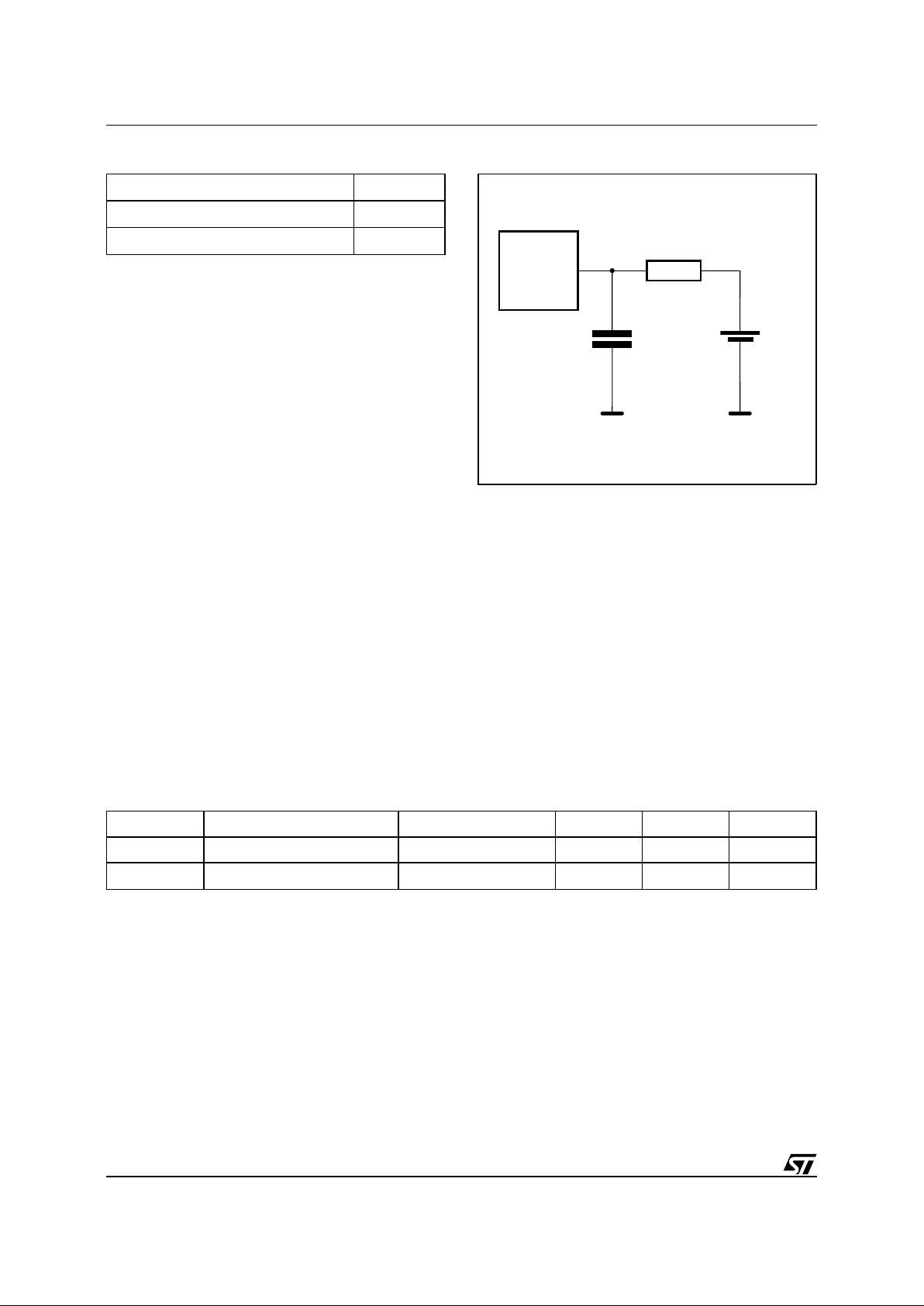
AI02394
V
CC
EE
CON
V
SS
V
OUT
V
CC
CMOS
SRAM
x8 or x16
3.3V or 5V
THS
E
0.1µF0.1µF
M40Z111
Thereshold
1N5817 or
MBR5120T3
Figure 3. Hardware Hookup
3/12
M40Z111, M40Z111W
Manufacturers generally specify a typical condition
for room temperature along with a worst case
condition (generally at elevated temperatures). The
system level requirements will determine the
choice of which value to use. The data retention
current value of the SRAMs can then be added to
the I
CCDR
value of the M40Z1 1 1/1 1 1W to det ermine
the total current requirements for data retention.
The available battery capacity for the SNAPHAT of
your choice can then be divided by this current to
determine the amount of dat a retention available
(see Table 7). For more information on Battery
Storage Life refer to the Application Note AN1012.
V
CC
NOISE AND NEGATIVE-GOING TRAN-
SIENTS
I
CC
transients, including those produced by output
switching, can produce voltage fluctuations, resulting in spikes on the V
CC
bus. These transients can
be reduced if capacitors are used to store energy,
which stabilizes the V
CC
bus. The energy stored in
the bypass capacitors will be released as low going
spikes are generated or energy will be absorbed
when overshoots occur.
Input Rise and Fall Times ≤ 5ns
Input Pulse Voltages 0 to 3V
Input and Output Timing Ref. Voltages 1.5V
Note that Output Hi-Z is defined as the point where data is no
longer driven.
T ab le 3. AC Measurement Condition
AI02326
CL = 100pF
or 5pF
CL includes JIG capacitance
645Ω
DEVICE
UNDER
TEST
1.75V
Figure 4. AC Testing Load Circuit
Symbol Parameter T est Condition Min Max Unit
C
IN
Input Capacitance VIN = 0V 8 pF
C
OUT
(2)
Output Capacitance V
OUT
= 0V 10 pF
Note:
1. Sampled only, not 100% tested.
2. Outputs deselected.
T ab le 4. Capacitance
(1)
(TA = 25°C; f = 1MHz)
A ceramic bypass capacitor value of 0.1µF (as
shown in Figure 4) is recommended in order to
provide the needed filtering. In addition to transients that are caused by normal SRAM operation,
power cycling can generate negative voltage
spikes on V
CC
that drive it to values below VSS by
as much as one volt. These neg ative spikes can
cause data corruption in the SRAM while in battery
backup mode. To protect from these voltage
spikes, ST recommends connecting a schottky diode from V
CC
to VSS (cathode connected to VCC,
anode to V
SS
).
4/12
M40Z1 11, M40Z111W
 Loading...