

5V or 3V NVRAM SUPERVISOR FOR LPSRAM
FEATURES SUMMARY
■ CONVERT LOW POWER SRAMs INTO
NVRAMs
■ 5V OR 3V OPERATING VOLTAGE
■ PRECISION POWER MONITORING and
POWER SWITCHING CIRCUITRY
■ AUTOMATIC WRITE-PROTECTION WHEN
V
IS OUT - OF-TOLERANC E
CC
■ CHOICE OF SUPPLY VOLTAGES and
POWER-FAIL DESELECT VOLTAGES:
– M40SZ100Y : V
4.20V ≤ V
PFD
– M40SZ100W: V
2.55V ≤ V
■ RESET OUTPUT (RST) FOR POWER ON
PFD
RESET
■ 1.25V REFERENCE (for PFI/PFO)
■ LESS THAN 10ns CHIP ENABLE ACCESS
PROPAGATION DELAY (at 5V)
■ OPTIONAL PACKA GING INCLUDES A 28-
LEAD SOIC and SNAPHAT
ordered separately)
■ 28-LEAD SOIC PAC KAG E PROVIDES
DIRECT CONNECTION FOR A SNAPHAT
TOP WHICH CONTAINS THE BATTERY
■ BATTERY LOW PIN (BL)
= 4.5 to 5.5V;
CC
≤ 4.50V
= 2.7 to 3.6V;
CC
≤ 2.70V
®
TOP (to be
M40SZ100Y
M40SZ100W
Figure 1. 16-pi n S O I C Package
16
1
SO16 (MQ)
Figure 2. 28-pi n S O I C Package*
SNAPHAT (SH)
Battery
28
1
SOH28 (MH)
* Contact Local Sales Office
Rev. 1.3
1/19September 2003

M40SZ100Y, M40SZ100W
TABLE OF CONTENTS
SUMMARY DESCRIPTION. . . . . . . . . . . . . . . . . . . . . . . . . . . . . . . . . . . . . . . . . . . . . . . . . . . . . . . . . . . 3
Logic Diagram (Figure 3.) . . . . . . . . . . . . . . . . . . . . . . . . . . . . . . . . . . . . . . . . . . . . . . . . . . . . . . . . . 3
Signal Names (Table 1.) . . . . . . . . . . . . . . . . . . . . . . . . . . . . . . . . . . . . . . . . . . . . . . . . . . . . . . . . . . 3
SOIC16 Connections (Figure 4.) . . . . . . . . . . . . . . . . . . . . . . . . . . . . . . . . . . . . . . . . . . . . . . . . . . . . 4
SOIC28 Connections (Figure 5.) . . . . . . . . . . . . . . . . . . . . . . . . . . . . . . . . . . . . . . . . . . . . . . . . . . . . 4
Block Diagram (Figure 6.) . . . . . . . . . . . . . . . . . . . . . . . . . . . . . . . . . . . . . . . . . . . . . . . . . . . . . . . . . 4
Hardware Hookup (Figure 7.) . . . . . . . . . . . . . . . . . . . . . . . . . . . . . . . . . . . . . . . . . . . . . . . . . . . . . . 5
MAXIMUM RATING. . . . . . . . . . . . . . . . . . . . . . . . . . . . . . . . . . . . . . . . . . . . . . . . . . . . . . . . . . . . . . . . . 5
Absolute Maximum Ratings (Table 2.) . . . . . . . . . . . . . . . . . . . . . . . . . . . . . . . . . . . . . . . . . . . . . . .5
DC AND AC PARAMETERS. . . . . . . . . . . . . . . . . . . . . . . . . . . . . . . . . . . . . . . . . . . . . . . . . . . . . . . . . . 6
DC and AC Measurement Conditions (Table 3.). . . . . . . . . . . . . . . . . . . . . . . . . . . . . . . . . . . . . . . . 6
AC Testing Load Circuit (Figure 8.). . . . . . . . . . . . . . . . . . . . . . . . . . . . . . . . . . . . . . . . . . . . . . . . . . 6
AC Testing Input/Output Waveforms (Figure 9.) . . . . . . . . . . . . . . . . . . . . . . . . . . . . . . . . . . . . . . . . 6
Capacitance (Table 4.) . . . . . . . . . . . . . . . . . . . . . . . . . . . . . . . . . . . . . . . . . . . . . . . . . . . . . . . . . . . 6
DC Characteristics (Table 5.) . . . . . . . . . . . . . . . . . . . . . . . . . . . . . . . . . . . . . . . . . . . . . . . . . . . . . . 7
OPERATION . . . . . . . . . . . . . . . . . . . . . . . . . . . . . . . . . . . . . . . . . . . . . . . . . . . . . . . . . . . . . . . . . . . . . . 8
Data Retention Lifetime Calculation . . . . . . . . . . . . . . . . . . . . . . . . . . . . . . . . . . . . . . . . . . . . . . .8
Power Down Timing (Figure 10.). . . . . . . . . . . . . . . . . . . . . . . . . . . . . . . . . . . . . . . . . . . . . . . . . . . . 9
Power Up Timing (Figure 11.) . . . . . . . . . . . . . . . . . . . . . . . . . . . . . . . . . . . . . . . . . . . . . . . . . . . . . 10
Power Down/Up AC Characteristics (Table 6.) . . . . . . . . . . . . . . . . . . . . . . . . . . . . . . . . . . . . . . . . 10
Power-on Reset Output . . . . . . . . . . . . . . . . . . . . . . . . . . . . . . . . . . . . . . . . . . . . . . . . . . . . . . . . . 11
Reset Input (RSTIN). . . . . . . . . . . . . . . . . . . . . . . . . . . . . . . . . . . . . . . . . . . . . . . . . . . . . . . . . . . . 1 1
RSTIN Timing Waveform (Figure 12.). . . . . . . . . . . . . . . . . . . . . . . . . . . . . . . . . . . . . . . . . . . . . . .11
Reset AC Characteristics (Table 7.) . . . . . . . . . . . . . . . . . . . . . . . . . . . . . . . . . . . . . . . . . . . . . . . . 11
Battery Low Pin . . . . . . . . . . . . . . . . . . . . . . . . . . . . . . . . . . . . . . . . . . . . . . . . . . . . . . . . . . . . . . . 12
Power-fail Input/Output . . . . . . . . . . . . . . . . . . . . . . . . . . . . . . . . . . . . . . . . . . . . . . . . . . . . . . . . . 12
V
Noise And Negative Going Transients. . . . . . . . . . . . . . . . . . . . . . . . . . . . . . . . . . . . . . . . . 12
CC
Supply Voltage Protection (Figure 13.) . . . . . . . . . . . . . . . . . . . . . . . . . . . . . . . . . . . . . . . . . . . . . . 12
PACKAGE MECHANICAL INFORMATION . . . . . . . . . . . . . . . . . . . . . . . . . . . . . . . . . . . . . . . . . . . . . 13
PART NUMBERING . . . . . . . . . . . . . . . . . . . . . . . . . . . . . . . . . . . . . . . . . . . . . . . . . . . . . . . . . . . . . . . 17
SNAPHAT® Battery Table (Table 13.) . . . . . . . . . . . . . . . . . . . . . . . . . . . . . . . . . . . . . . . . . . . . . .17
REVISION HISTORY. . . . . . . . . . . . . . . . . . . . . . . . . . . . . . . . . . . . . . . . . . . . . . . . . . . . . . . . . . . . . . . 18
2/19
SUMMARY DESCRIPTION
The M40SZ100Y/W NVRAM Controller is a selfcontained device which converts a standard lowpower SRAM into a non-volatile mem ory. A prec ision voltage reference and comparator monitors
the V
When an invalid V
tioned chip enable output (E
input for an out-of-tolerance condition.
CC
condition occurs, t he condi-
CC
) is forced inactive
CON
to write protect the stored data in the SRAM. During a power failure, the SRAM is switched from the
pin to the lithium cell within the SNAPHAT (or
V
CC
external battery for the 16-lead S OIC) to provide
the energy required for data retention. On a subsequent power-up, the SRAM remains write protected until a valid power condition returns.
The 28-pin, 330 mil SOIC provides soc kets with
gold plated contacts for direct connection to a separate SNAPHAT
®
housing containing the battery.
The SNAPHAT housing has gold plated pins
which mate with the sockets, ensuring reliable
connection. The housing is keyed to prevent improper insertion. This unique design allows the
SNAPHAT battery p acka ge t o be m ount ed o n t op
M40SZ100Y, M40SZ100W
of the SOIC package after the c ompletion of the
surface mount process which greatly reduces the
board manufacturing process complexity of either
directly soldering or inserting a battery into a soldered holder. Providing non-volatility becomes a
“SNAP.” This feature is also a vailable in the “topless” 16-pin SOIC package (MQ).
Insertion of the SNAPHAT housing after reflow
prevents potential battery damage due to the high
temperatures required for device surface-moun ting. The SNAPHA T housing is also k eyed to prevent reverse insertion.
The 28-pin SOIC and battery packages are
shipped separately in plastic anti-static tubes or in
Tape & Reel form. For the 2 8-lead SOIC, t he ba ttery/crystal package (e.g., SNAPHAT) part number is “M4ZXX-BR00SH” (see Table 13, page 17).
Caution: Do not place the SNAPHAT battery top
in conductive foam, as this will drain the lithium
button-cell battery.
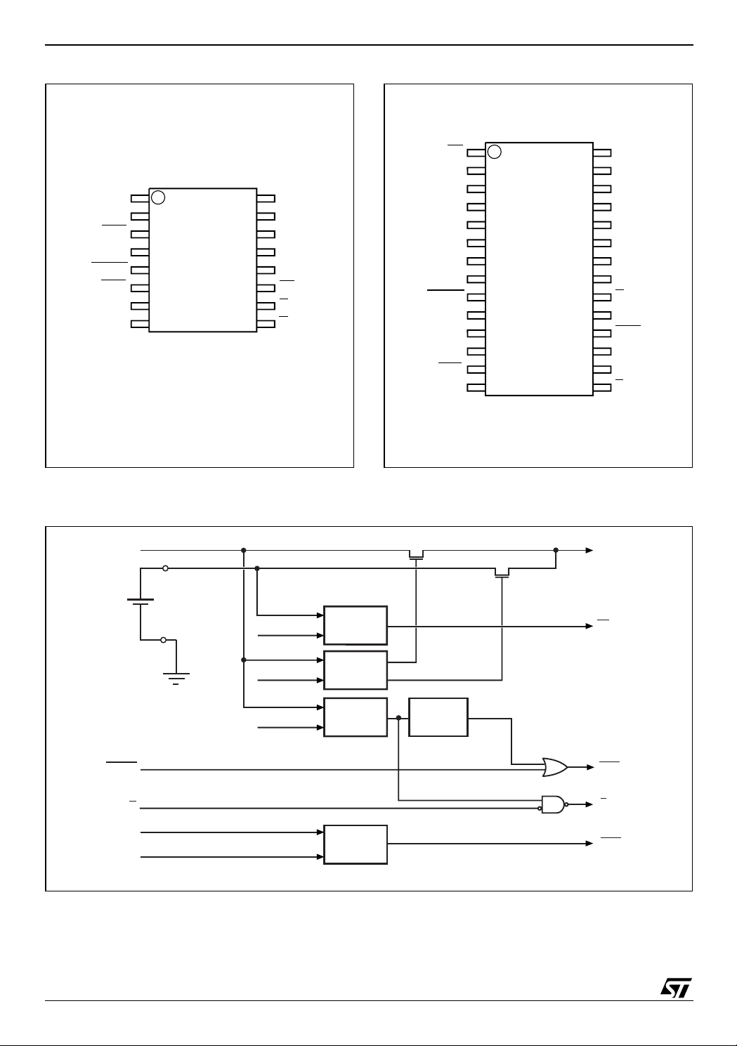
Figure 3. Logic Diagram
V
V
E
PFI
RSTIN
Note: 1. For 16-pin SOIC pac kage only.
M40SZ100Y
M40SZ100W
V
CC
SS
BAT
(1)
V
OUT
BL
E
CON
PFO
RST
AI03933
Table 1. Signal Names
E Chip Enable Input
E
CON
RST
RSTIN
BL
V
OUT
V
CC
(1)
V
BAT
PFI Power Fail Input
PFO
V
SS
NC Not Connected Internally
Note: 1. For SO1 6 onl y.
Conditioned Chip Enable Output
Reset Output (Open Drain)
Reset Input
Battery Low Output (Open Drain)
Supply Voltage Output
Supply Voltage
Back-up Supply Voltage
Power Fail Output
Ground
3/19
M40SZ100Y, M40SZ100W
Figure 4. SOI C 16 Connection s
NC
NC
RST
NC
RSTIN
PFO
V
BAT
V
SS
Note: 1. DU = Do Not Use
1
2
3
4
M40SZ100Y
M40SZ100W
5
6
710
8
16
15
14
13
12
11
Figure 5. SOI C 28 Connection s
1
BL
NC
V
CC
NC
V
OUT
NC
PFI
BL
E
E
9
CON
AI03935
NC
NC
NC
NC
NC
NC
RSTIN
NC
NC
PFO
V
SS
2
3
4
5
6
7
M40SZ100Y
M40SZ100W
8
9
10
11
12
13
14
28
27
26
25
24
23
22
21
20
19
18
17
16
15
AI03934
V
CC
NC
NC
V
OUT
NC
NC
PFI
NC
E
NC
RST
NCNC
NC
E
CON
Figure 6. Block Diagram
V
CC
V
BAT
RSTIN
E
PFI
1.25V
Note: Open dra i n output
VBL= 2.5V
V
= 2.5V
SO
V
= 4.4V
PFD
COMPARE
COMPARE
COMP ARE
(2.65V for SZ100W)
COMPARE
POR
V
OUT
(1)
BL
RST
E
CON
PFO
AI04766
(1)
4/19
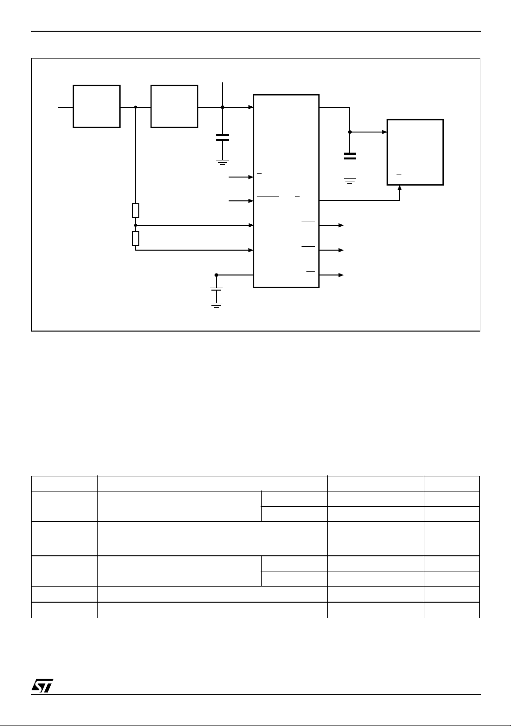
Figure 7. Hardware Hookup
M40SZ100Y, M40SZ100W
3.0V, 3.3V or 5V
Unregulated
Voltage
R1
R2
Note: 1. User supplied for the 16-pin pa ck age
Regulator
V
IN
From Microprocessor
V
CC
0.1µF
V
CC
E
RSTIN
PFI
V
SS
V
BAT
V
OUT
M40SZ100Y
M40SZ100W
E
CON
PFO
(1)
RST
BL
V
CC
0.1µF
To Microprocessor NMI
To Microprocessor Reset
To Battery Monitor Circuit
1Mb or 4Mb
LPSRAM
E
AI04767
MAXIMUM RATI N G
Stressing the device ab ove the rating listed in t he
“Absolute Maximum Ratings” table may cause
permanent damage to the device. These are
stress ratings only and operation of the dev ice at
these or any other conditions above those indicat-
not implied. Exposure to Absol ute Maxim um Ra ting conditions for extended periods may affect device reliability. Refer also to the
STMicroelectronics SURE Program and other relevant quality documents.
ed in the Operating sections of this specification is
Table 2. Absolute Maximum Ratings
Symbol Parameter Value Unit
T
STG
(1)
T
SLD
V
IO
V
CC
I
O
P
D
Note: 1. Reflow at peak temperature of 215°C to 225°C for < 60 seconds (total thermal budget not to ex ceed 180°C for between 90 to 120
secon ds).
CAUTION: Negative und ershoots below –0.3V are not allowed on any pin while in the Battery Ba ck-up mod e.
CAUTION: Do NOT wave solder SOIC to avoid damaging SNAP HAT sock ets.
Storage Temperature (VCC Off)
Lead Solder Temperature for 10 seconds 260 °C
Input or Output Voltages
Supply Voltage
Output Current 20 mA
Power Dissipation 1 W
SNAPHAT –40 to 85 °C
SOIC –55 to 125 °C
–0.3 to V
CC
+0.3
M40SZ100Y –0.3 to 7 V
M40SZ100W –0.3 to 4.6 V
V
5/19
M40SZ100Y, M40SZ100W
DC AND AC PARAMETERS
This section summarizes the operat ing and measurement conditions, as well as the DC and AC
characteristics of the device. The parameters in
the following DC and AC Characteristic tables are
derived from tests performed under the M easure-
Table 3. DC and AC Measurement Conditions
Parameter M40SZ100Y M40SZ100W
Supply Voltage
V
CC
Ambient Operating Temperature –40 to 85°C –40 to 85°C
ment Conditions listed in the rel evant tables. Designers should check that the operating conditions
in their projects match the measurement conditions when using the quoted parameters.
4.5 to 5.5V 2.7 to 3.6V
Load Capacitance (C
)
L
100pF 50pF
Input Rise and Fall Times ≤ 5ns ≤ 5ns
Input Pulse Voltages
Input and Output Timing Ref. Voltages
Figure 8. AC Testing Load Circuit
DEVICE
UNDER
TEST
CL includes JIG capacitance
333Ω
CL = 100pF
or 50pF
1.73V
AI02393
0.2 to 0.8V
0.3 to 0.7V
CC
CC
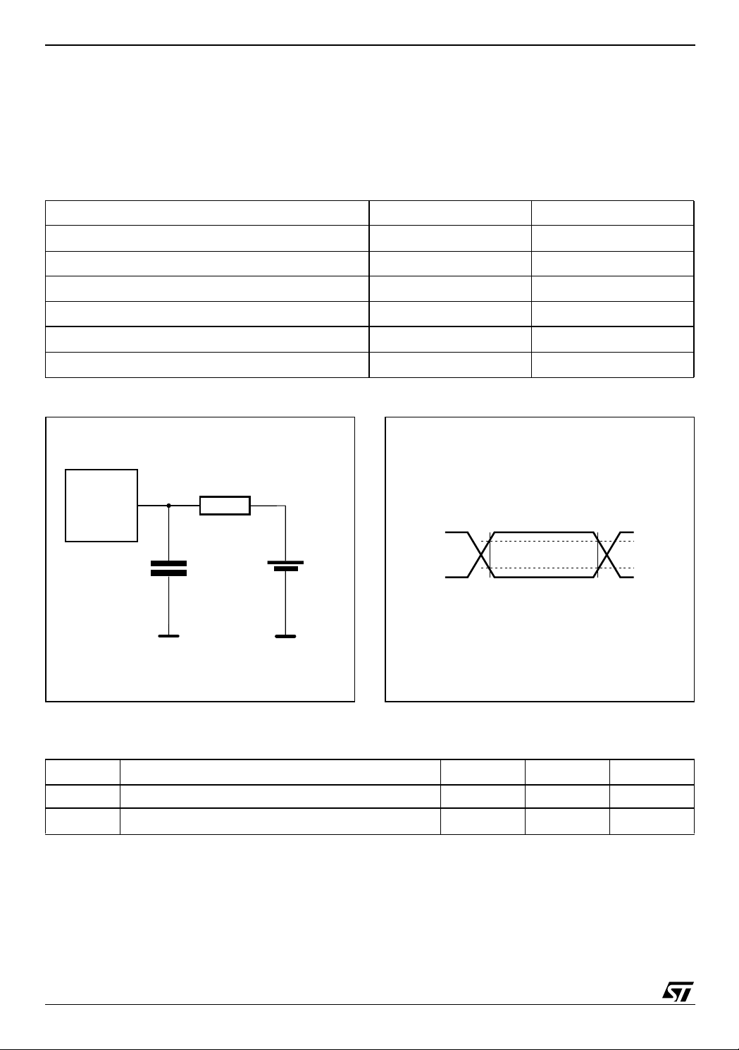
Figure 9. AC Testing Input/Output Waveforms
0.8V
CC
0.2V
CC
0.2 to 0.8V
0.3 to 0.7V
CC
CC
0.7V
0.3V
AI02568
CC
CC
Note: 1. CL = 100pF for M40SZ100Y and 50pF for M40SZ100W.
Table 4. Capacitance
Symbol
C
IN
C
OUT
Note: 1. Sampled only, not 100% tested.
2. At 25°C, f = 1MHz.
3. Outpu ts deselected
Input Capacitance 7 pF
(3)
Output Capacitance 10 pF
6/19
Parameter
(1,2)
Min Max Unit

M40SZ100Y, M40SZ100W
Table 5. DC Characteristics
Sym Parameter
I
Supply Current Outputs open 1 0.5 mA
CC
I
CCDR
Data Retention Mode
(2)
Current
Input Leakage
Current
(3)
I
LI
Input Leakage
Test Condition
0V ≤ V
(1)
≤ V
IN
CC
Current (PFI)
I
LO
I
OUT1
I
OUT2
V
V
V
V
V
V
(4)
Current
V
Current
OUT
(5)
(Active)
V
Current
OUT
(Battery Back-up)
Battery Voltage 2.5 3.0
BAT
V
Input High Voltage
IH
V
Input Low Voltage –0.3
IL
Output High
OH
OHB
(7)
Voltage
VOH Battery Back-
(8)
up
Output Low Voltage
OL
Output Low Voltage
(open drain)
Power-fail Deselect
PFD
Voltage
(9)
PFI Input Threshold
PFI
0V ≤ V
V
OUT
V
OUT
IOH = –1.0mA
I
OUT2
I
V
V
≤ V
OUT
> VCC – 0.3
> V
– 0.3
BAT
= –1.0µA
= 3.0mA
OL
IOL = 10mA
= 5V(Y)
CC
= 3V(V)
CC
CC
Output Leakage
PFI Hysteresis PFI Rising 20 70 20 70 mV
V
Note: 1. Valid fo r Ambient Op erating Temperature: TA = –40 to 85°C ; VCC = 2.7 to 3.6V or 4. 5 to 5.5V(exc ept where not ed).
Battery Back-up
SO
Switchover Voltage
2. Measured with V
3. RSTIN
4. Outpu ts deselected.
5. External SRAM must match SUPERVISOR chip V
6. For rechargeabl e back-up, V
7. For PFO
8. Chip Enable output (E
9. For RST
internally pulled-up to VCC through 100kΩ resis tor.
pin (CMOS).
duce batter y li fe.
& BL pins (Open Drain).
OUT
and E
CON
open.
CON
(max) may be considered VCC – 0.5V.
BAT
) can only sust ai n CMOS leakage currents i n the battery back-up mode. Higher leakag e currents wi ll re-
specification (3V or 5V).
CC
M40SZ100Y M40SZ100W
Min Typ Max Min Typ Max
50 200 50 200 nA
±1 ±1 µA
–25 2 25 –25 2 25 nA
±1 ±1 µA
175 100 mA
100 100 µA
0.7V
CC
(6)
3.5
VCC + 0.3 0.7V
0.3V
CC
2.5 3.0
CC
–0.3
3.5
VCC + 0.3
0.3V
2.4 2.4 V
2.5 2.9 3.5 2.5 2.9 3.5 V
0.4 0.4 V
0.4 0.4 V
4.20 4.40 4.50 2.55 2.60 2.70 V
1.225 1.250 1.275 1.225 1.250 1.275 V
2.5 2.5 V
(6)
CC
Unit
V
V
V
7/19

M40SZ100Y, M40SZ100W
OPERATION
The M40SZ100Y/W, as shown in Figure 7, page 5,
can control one (two, if placed in parallel) standard
low-power SRAM. This SRAM must be configured
to have the chip enable input disable all other input
signals. Most slow, low-power SRAM s are c onfigured like this, however many fast SRAM s are not.
During normal operating conditions, the conditioned chip enable (E
chip enable (E
) input pin with timing shown in Table 6, page 10. An internal switch connects V
V
. This switch has a voltage drop of less than
OUT
0.3V (I
When V
).
OUT1
degrades during a power failure, E
CC
is forced inactive independe nt of E. In t his situa tion, the SRAM is unconditionally write protected
as V
(V
falls below an out-of-tolerance threshold
CC
). For the M40SZ100Y/W the power fail de-
PFD
tection value associated with V
ble 5, page 7.
If chip enable access is in progress during a power
fail detection, that memory cycle continues to completion before the memory is write protected. I f the
memory cycle is not terminated within time t
E
is unconditionally driven high, write protect-
CON
ing the SRAM. A power failure during a WRITE cycle may corrupt data at the currently addressed
location, but does not jeopardize the rest of the
SRAM's contents. At voltage s below V
the user can be as sured the me mor y will be writ e
protected within the Write Protect Time (t
vided the V
fall time does not exceed tF (see Ta-
CC
ble 6, page 10).
As V
disconnects V
to V
(V
age V
I
OUT2
When V
continues to degrade, the internal switch
CC
. This occurs at the switchover voltage
OUT
). Below the VSO, the battery provides a volt-
SO
OHB
and connects the internal battery
CC
to the SRAM and can supply current
(see Table 5, page 7).
rises above VSO, V
CC
back to the supply voltage. Output E
active for t
(120ms maxim um ) af ter t he power
CER
) output pin follows the
CON
is shown in Ta-
PFD
PFD
is switched
OUT
CON
to
CC
CON
WPT
(min),
) pro-
WPT
is held in-
supply has reached V
, independent of the E in-
PFD
put, to allow for processor stabilization (see Figure
11, page 10).
Data Retention Lifetime Calculation
Most low power SRAMs on the market today can
be used with the M40SZ100Y/W NVRAM Controller. There are, however some criteria which should
be used in making the final choice of which SRAM
to use. The SRAM must be designed in a way
where the chip enable input disables all other inputs to the SRAM. This allows inputs to the
M40SZ100Y/W and SRAMs to be “Don't care”
once V
falls below V
CC
(min) (see Figure 10,
PFD
page 9). The SR AM should also guarantee data
retention down to V
= 2.0V. The chip enable ac-
CC
cess time must be sufficient to meet the system
needs with the chip enable propagation delays included.
If data retention lifetime is a critical parameter f or
the system, it is importa nt to re view the dat a retention current specifications for the particular
SRAMs being evaluated. M ost SRAMs specify a
,
data retention current at 3.0V. Manufacturers generally specify a typical condition for room temperature along with a worst case condition (generally
at elevated temperatures). The system level requirements will determine the choice of which value to use. The data retent ion current val ue of the
SRAMs can then be added to t he I
CCDR
the M40SZ100Y/W to determine the to tal current
requirements for data retention. The available battery capacity for the SNAPHAT
®
of your choice
(see Table 13, page 17) can then be divided by
this current to determine the amount of data retention available.
CAUTION: Take care to avoid inadvertent discharge through V
OUT
and E
after battery has
CON
been attached.
For a further more detailed review of lifetime calcu-
lations, please see Application Note AN1012.
value of
8/19

Figure 10. Power Down Timing
V
CC
V
(max)
PFD
V
PFD
V
(min)
PFD
VSO
tF
E
E
CON
RST
tWPT
tFB
V
M40SZ100Y, M40SZ100W
OHB
PFO
VALID
AI03936
9/19

M40SZ100Y, M40SZ100W
Figure 11. Power Up Timing
V
CC
V
(max)
PFD
V
PFD
V
(min)
PFD
VSO
tR
E
E
CON
RST
PFO
tRB
V
OHB
tCER
tREC
VALID
Table 6. Power Down/Up AC Characteristics
Symbol
(2)
t
F
(3)
t
FB
t
PFD
t
R
t
EPD
t
RB
t
CER
t
REC
t
WPT
Note: 1. Valid fo r Ambient Op erating Temperature: TA = –40 to 85°C ; VCC = 2.7 to 3.6V or 4. 5 to 5.5V(exc ept where not ed).
2. V
3. V
V
(max) to V
PFD
V
(min) to VSS VCC Fall Time
PFD
PFD
PFI to PFO Propagation Delay 15 25 µs
V
(min) to V
PFD
PFD
Chip Enable Propagation Delay (Low or High)
VSS to V
(min) VCC Rise Time
PFD
Chip Enable Recovery 40 120 ms
V
(max) to RST High
PFD
Write Protect Time 40 200 µs
(max) to V
PFD
passes V
PFD
(min) to VSS fall time of le ss than tFB may cause corruption of RAM d at a.
PFD
(min) fall ti me of less th an tF may result in deselect ion/writ e protec tion not oc currin g until 20 0 µs after V
PFD
(min).
Parameter
(min) VCC Fall Time
(max) VCC Rise Time
(1)
Min Max Unit
300 µs
10 µs
10 µs
M40SZ100Y 10 ns
M40SZ100W 15 ns
1µs
40 200 ms
tEPDtEPD
AI03937
CC
10/19

M40SZ100Y, M40SZ100W
Power-on Reset Output
All microprocessors have a reset input which forces them to a known state when starting. The
M40SZ100Y/W has a reset output (RST
is guaranteed to be low by V
PFD
) pin which
(see Table 5,
page 7). This signal is an open drain configuration.
An appropriate pull-up resistor to V
should be
CC
chosen to control the rise time. This signal will be
valid for all voltage conditions, even when V
CC
equals VSS (with valid battery voltage).
Once V
age V
t
REC
Figure 12. RSTIN
Note: With pul l -up resi stor
exceeds the power failure detect volt-
CC
, an internal timer keeps RST low for
PFD
to allow the power supply to stabilize.
Timing Waveform
RSTIN
tRLRH
(1)
RST
tR1HRH
Reset Input (RSTIN
)
The M40SZ100Y/W provides one indep endent input which can generate an output reset. The duration and function of this reset is identical to a reset
generated by a power cycle. Table 7 and Figure 12
illustrat e the AC rese t ch ara cterist ics of t his f unction. Pulses shorter than t
reset condition. RSTIN
V
through a 100kΩ resistor.
CC
is internally pulled up to
will not generate a
RLRH
AI04768
Table 7. Reset AC Characteristics
Symbol
(2)
t
RLRH
(3)
t
R1HRH
Note: 1. Valid fo r Ambient Op erating Temperature: TA = –40 to 85°C ; VCC = 2.7 to 3.6V or 4. 5 to 5.5V (exce pt where not ed).
2. Pulse width less than 50ns will result in no RESET (for noise immunity).
= 5pF (see Figure 8, page 6).
3. C
L
RSTIN Low to RSTIN High 200 ns
RSTIN High to RST High 40 200 ms
Parameter
(1)
Min Ma x Unit
11/19

M40SZ100Y, M40SZ100W
Battery Low Pin
The M40SZ100Y/W automatically performs battery voltage monitoring upon power-up, and at factory-programmed time intervals of at least 24
hours. The Battery Low (BL
the battery voltage is found to be less than approximately 2.5V. The BL
completion of battery replacement and subsequent battery low monitoring tests, either during
the next power-up sequence or the next scheduled
24-hour interval.
If a battery low is generated during a power-up sequence, this indicates that the battery is below
2.5V and may not be able to maintain data integrity
in the SRAM. Data should be considered suspect,
and verified as correct. A fresh battery should be
installed.
If a battery low indication is generated during the
24-hour interval check, this indicates that the battery is near end of life. However, data is not compromised due to the fact that a nominal V
supplied. In order to insure data integrity during
subsequent periods of bat tery back-up m ode, the
battery should be replaced.
The M40SZ100Y/W only monitors the battery
when a nominal V
is applied to the device. Thus
CC
applications which require extensive d urations in
the battery back-up mode sho uld be pow ered-up
periodically (at least once every few months) in order for this technique to be beneficial. Additionally,
if a battery low is indicated, data integrity should
be verified upon power-up via a checksum or other
technique. The BL
pin is an open drain output and
an appropriate pull-up resistor to V
chosen to control the rise time.
Power-fail Input/Output
The Power-Fail Input (PFI) is compared to an internal reference voltage (independent from the
comparator). If PFI is less than the power-fail
V
PFD
threshold (V
), the Power-Fail Output (PFO) will
PFI
go low. This function is intended for use as an under-voltage detector to signal a failing power supply. Typically PFI is connected through an external
voltage divider (see Figure 7, page 5) to either the
unregulated DC input (if it is a va ilable) or the regulated output of the V
vider can be set up such that t he voltage at PFI
falls below V
regulated V
several milliseconds before the
PFI
input to the M40SZ100Y /W or the
CC
microprocessor drops below the minimum operating voltage.
During battery back-up, the power-fail comparator
turns off and PFO
goes (or remains) low. This oc-
) pin will be asserted if
pin will remain asserted until
is
CC
should be
CC
regulator. The voltage di-
CC
curs after V
er returns, PFO
for the write protect time (t
from V
PFD
drops below V
CC
is forced high, irrespective of V
(min). When pow-
PFD
), which is the time
REC
PFI
(max) until the inputs are recognized. At
the end of this time, the power-fail comparator is
enabled and PFO
unused, PFI should be connected to V
follows PFI. If the comparator is
and PFO
SS
left unconnected.
Noise And Negative Going Transients
V
CC
transients, including those produced by output
I
CC
switching, can produce voltage fluctuations, resulting in spikes on the V
bus. These transients
CC
can be reduced if capacitors are used to store energy which stabilizes the V
bus. The energy
CC
stored in the bypass capacitors will be released as
low going spikes are generated or energy will be
absorbed when overshoots occur. A ceramic bypass capacitor value of 0.1µF (as shown in Figure
13) is recommended in order to provide the needed filtering.
In addition to transients that are caused by normal
SRAM operation, power cycling can generate negative voltage spikes on V
below V
by as much as one volt. These negative
SS
that drive it to values
CC
spikes can cause data corruption in the SRAM
while in battery backup mode. To protect from
these voltage spikes, STMicroelectronics recommends connecting a schottky diode from V
V
(cathode connected to VCC, anode to VSS).
SS
CC
to
Schottky diode 1N5817 is recommended for
through hole and MBRS120T3 is recommended
for surface mount.
Figure 13. Supply Voltage Protection
V
CC
V
CC
0.1µF DEVICE
V
SS
AI00622
12/19

PACKAGE MECHANICAL INFORMATION
Figure 14. SO16 – 16-lead Plastic Small Package Outline
M40SZ100Y, M40SZ100W
A2
A
B
e
CP
D
N
E
H
1
SO-b
Note: Drawing is not to scale.
Table 8. SO16 – 16-lead Plastic Small Plastic Package Mechanical Data
Symbol
T yp. Min. Max. Typ. Min. Max.
A 1.75 0.069
mm inches
C
LA1 α
A1 0.10 0.25 0.004 0.010
A2 1.60 0.063
B 0.35 0.46 0.014 0.018
C 0.19 0.25 0.007 0.010
D 9.80 10.00 0.386 0.394
E 3.80 4.00 0.150 0.158
e 1.27 – – 0.050 – –
H 5.80 6.20 0.228 0.244
L 0.40 1.27 0.016 0.050
a0°8°0°8°
N16 16
CP 0.10 0.004
13/19

M40SZ100Y, M40SZ100W
Figure 15. SOH28 – 28-lead Plastic Small Outline, 4-socket battery SNAPHAT, Package Outline
A2
A
C
Be
eB
CP
D
N
E
H
LA1 α
1
SOH-A
Note: Drawing is not to scale.
Table 9. SOH28 – 28-lead Plastic Sm al l Outl ine, bat tery SNAP HAT, Pac kage Mech an ical Data
Symbol
T yp Min Max Typ Min Max
A 3.05 0.120
A1 0.05 0.36 0.002 0.014
mm inches
A2 2.34 2.69 0.092 0.106
B 0.36 0.51 0.014 0.020
C 0.15 0.32 0.006 0.012
D 17.71 18.49 0.697 0.728
E 8.23 8.89 0.324 0.350
e 1.27 – – 0.050 – –
eB 3.20 3.61 0.126 0.142
H 1 1.51 12.70 0.453 0.500
L 0.41 1.27 0.016 0.050
α 0° 8° 0° 8°
N 28 28
CP 0.10 0.004
14/19

M40SZ100Y, M40SZ100W
Figure 16. SH – 4-pin S NAPHAT Ho using fo r 48mAh Ba ttery , Package Outline
A1
A
eA
D
B
eB
E
SHZP-A
Note: Drawing is not to scale.
Table 10. SH – 4-pin SNAPHAT Housing for 48mAh Battery, Package Mechanical Data
Symbol
Typ Min Max Typ Min Max
A 9.78 0.385
A1 6.73 7.24 0.265 0 .285
mm inches
A2
A3
L
A2 6.48 6.99 0.255 0 .275
A3 0.38 0.015
B 0.46 0.56 0.018 0.022
D 21.21 21.84 0.835 0 .860
E 14.22 14.99 0.560 0.590
eA 15.55 15.9 5 0.612 0.628
eB 3.20 3.61 0.126 0 .142
L 2.03 2.29 0.080 0 .090
15/19

M40SZ100Y, M40SZ100W
Figure 17. SH – 4-pi n SNAP HAT Housing for 12 0mAh B attery , Package Outline
A1
A
eA
D
B
eB
E
SHZP-A
Note: Drawing is not to scale.
Table 11. SH – 4-pin SNAPHAT Housing for 120mAh Battery, Package Mechanical Data
Symbol
Typ Min Max Typ Min Max
A 10.54 0.415
A1 8.00 8.51 0.315 0 .335
mm inches
A2
A3
L
A2 7.24 8.00 0.285 0 .315
A3 0.38 0.015
B 0.46 0.56 0.018 0.022
D 21.21 21.84 0.835 0 .860
E 17.27 18.03 0.680 0.710
eA 15.55 15.9 5 0.612 0.628
eB 3.20 3.61 0.126 0 .142
L 2.03 2.29 0.080 0 .090
16/19

M40SZ100Y, M40SZ100W
PART NUMBERING
Table 12. Ordering Information Scheme
Example: M40SZ 100Y MQ 6 TR
Device Type
M40SZ
Supply Voltage and Write Protect Voltage
100Y = V
100W = V
Package
MQ = SO16
(1,2)
MH
= 4.5 to 5.5V; V
CC
= 2.7 to 3.6V; V
CC
= SOH28
= 4.2 to 4.5V
PFD
= 2.6 to 2.7V
PFD
Temperature Rang e
6 = –40 to 85°C
Shipping Method for SOIC
blank = Tubes
TR = Tape & Reel
Note: 1. The SOIC packa ge (SOH28) require s the battery pack age (SNAPHAT®) which is o rdered separately under the part numbe r
“M4ZXX-BR00SHX” in plastic tube or “M4ZXX-BR00SHXTR” in Tape & Reel form.
2. Contact Local Sal es Off ice
Caution: Do not place the SNAPHAT battery package “M4Zxx-BR00SH” in conductive foam as it will drain the lithium button-cell bat-
tery.
For a list of available options (e.g., Speed, Package) or for further information on any aspect of this device,
please contact the ST Sales Office nearest to you.
®
Table 13. SNAPHAT
Part Number Description Package
M4Z28-BR00SH SNAPHAT Housing for 48mAh Battery SH
M4Z32-BR00SH SNAPHAT Housing for 120mAh Battery SH
Battery Ta bl e
17/19

M40SZ100Y, M40SZ100W
REVISION HIST ORY
Table 14. Document Revision History
Date Rev. # Revision Details
December 2001 1.0 First Issue
13-May-02 1.1 Modify reflow time and temperature footnote (Table 2)
01-Aug-02 1.2 Add marketing status (Figure 2; Table 12)
15-Sep-03 1.3 Remove reference to M68xxx (obsolete) part (Figure 7); update disclaimer
18/19

M40SZ100Y, M40SZ100W
M40SZ100, M40SZ100Y, M40SZ100W, 40SZ100, 40SZ100Y, 40SZ100W, ZEROPOWER, ZEROPOWER, ZEROPOWER, ZEROPOWER, ZEROPOWER, ZEROPOWER, ZEROPOWER, ZEROPOWER, ZEROPOWER, ZEROPOWER,
ZEROPOWER, ZEROPOWER, ZEROPOWER, ZEROPOWER, ZEROPOWER, SUPERVISOR, SUPER VISOR, SUPERVISOR, SUPERVISOR, SUPERVISOR, SUPERVISOR, SUPERVISOR, SUPERVISOR, SUPERVISOR, SUPERVISOR, SUPERVISOR, SUPERVISOR, SUPERVISOR, SUPERVISOR, SUPERVISOR, NVRAM, NVRAM, NVRAM,
NVRAM, NVRAM, NVRAM, NVRAM, NVRAM, NVRAM, NVRAM, NVRAM, NVRAM, NVRAM, NVRAM, NVRAM,
NVRAM, NVRAM, NVRAM, NVRAM, NVRAM, NVRAM, NVRAM, NVRAM, NVRAM, NVRAM, NVRAM, NVRAM,
NVRAM, NVRAM, NVRAM, NVRAM, NVRAM, NVRAM, NVRAM, NVRAM, NVRAM, NVRAM, NVRAM, NVRAM,
NVRAM, NVRAM, NVR AM, NVRAM, NVRAM, NVR AM, NVRAM, NVRAM, NVR AM, NVRAM, NVRAM, I2C , I2C, I2C,
I2C, I2C, I2C, I2C, I2C, I2C, I2C, I2C, I2C, I2C, I2C, I2C, I2C, I2C, I2C, I2C, I2C, I2C, I2C, I2C, I2C, I2C, I2C, I2C, I2C,
I2C, I2C, I2C, I2C, I2C, I2C, I2C, I2C, I2C, I2C, I2C, I2C, I2C, I2C, I2C, I2C, I2C, RTC, RTC, RTC, RTC, RTC, RTC, RTC,
RTC, RTC, RTC, RTC, RTC , RTC, RTC, RTC, RT C, RTC, RTC, RTC , RTC, RTC, RTC, RTC , RTC, RTC, RTC, RTC,
RTC, RTC, RTC, RTC, RTC , RTC, RTC, RTC, RT C, RTC, RTC, RTC , RTC, RTC, RTC, RTC , RTC, RTC, RTC, RTC,
RTC, RTC, RTC, RTC, RTC, RTC, RTC, RTC, RTC, RTC, RTC, RTC, RTC, RTC, RTC, RTC, RTC, RTC, Oscillator, Oscillator, Oscillator, Osc illator, Oscillat or, Oscillator, Os cillator, Oscilla tor, Oscillator , Oscillator, Oscil lator, Oscillato r, Oscillator, Oscillator, Oscillator, Oscillator, Oscillator, Oscillator, Oscillator, Oscillator, Oscillator, Oscillator, Oscillator,
Oscillator, Oscilla tor, Oscillator, Oscillator , Oscillator, Oscillator, O scillator, Oscillator, Osci llator, Oscillator, Oscillator,
Oscillator, Micropr ocessor, Microprocessor, Microp rocessor, Microprocessor, Micro processor, Microprocessor, Mic roprocessor, Micropro cessor, Microprocessor, Mic roprocessor, Microproce ssor, Microprocessor, Microproce ssor, Microprocessor, Microprocessor, Microprocessor, Microprocessor, Microprocessor, Microprocessor, Microprocessor,
LPSRAM, LPSRAM, LPSRAM, LPSRAM, LPSRAM, LPSRAM, LPSRAM, LPSRAM, LPSRAM, LPSRAM, LPSRAM,
LPSRAM, LPSR AM, LPSR AM, LPSR AM, P FI, P FI, P FI, PFI, PF I, PF I, PF I, PFI , PFI, PFI, PFI, PFI, PFI, P FI, P FI, P FI,
PFI, PFI, PFI, PFI, PFI, PFI, PFI, PFI, PFI, PFI, PFI, PFI, PFI, PFI, PFI, PFI, PFI, PFI, PFI, PFO, PFO, PFO, PFO, PFO,
PFO, PFO, P FO, PFO , PFO, PFO, PF O, PFO, PFO, P FO, PFO , PFO, PFO, PF O, PFO, Reset, Reset, Re set, Res et,
Reset, Reset, Reset, Reset, Reset, Reset, Reset, Reset, Reset, Reset, Reset, Reset, Reset, Reset, Reset, Reset, Reset,
Reset, Reset, Reset, Reset, Reset, Reset, Reset, Reset, Reset, Reset, Reset, Reset, Reset, Reset, Reset, Reset, Reset,
Reset, Reset, Reset, Reset, Reset, Reset, Reset, Reset, Reset, Reset, Reset, Reset, Reset, Reset, Reset, Reset, Reset,
Reset, Reset, Reset, Reset, Reset, Reset, Reset, Reset, Reset, Reset, Reset, Reset, Reset, Reset, Reset, Reset, Reset,
Reset, Reset, Reset, Reset, Reset, Reset, Reset, Reset, Reset, Reset, Reset, Reset, Reset, Reset, Reset, Reset, Reset,
Reset, Reset, Reset, Reset, Reset, Reset, Write Protect, Write Protect, Write Protect, Write Protect, Write Protect, Write
Protect, Write Protect, Writ e Protect , Write Prote ct, Write Pro tect, Writ e Protect , Write Protect, Write Pro tect, Writ e Protect, Write Protect, Write Prote ct, Write Pro tect, Writ e Protec t, Write Prote ct, Write Pro tect, Writ e Protect, Write Prote ct,
Write Protect, Write Pro tect, Writ e Pr otect , Ba ttery, Batt ery, Batte ry, Batter y, B attery , Ba ttery, Bat tery, Batt ery, Batte ry,
Battery, Battery, Batte ry, Battery, Battery, Batte ry, Battery, Battery, Battery, Batte ry, Battery, Battery, Batte ry, Battery,
Battery, Battery, Batte ry, Battery, Battery, Batte ry, Battery, Battery, Battery, Batte ry, Battery, Battery, Batte ry, Battery,
Battery, Battery, Batte ry, Battery, Battery, Batte ry, Battery, Battery, Battery, Batte ry, Battery, Battery, Batte ry, Battery,
Battery, Battery, Battery, Battery, Battery, Battery, Battery, Battery, Battery, Switchover, Switchover, Switchover,
Switchover, Switchover, Switchover, Switchover, Switchover, Switchover, Switchover, Power-fail, Power-fail, Power-fail,
Power-fail, Powe r-fail, Pow er-fail, Pow er-fail, Pow er-fail, Pow er-fail, Pow er-fail, Com parator, C omparator , Comparat or,
Comparator, C omparator, Compara tor, Comp arator, Co mparator, Compara tor, Comp arator, Co mparator, Comparat or,
Comparator, C omparator, Compara tor, Comp arator, Co mparator, Compara tor, Comp arator, Co mparator, Comparat or,
Comparator, C omparator, Compara tor, Comp arator, Co mparator, Compara tor, Comp arator, Co mparator, Comparat or,
Comparator, C omparator, Compara tor, Comp arator, Co mparator, Compara tor, Comp arator, Co mparator, Comparat or,
Comparator, Comparator, Comparator, Comparator, Comparator, Comparator, SNAPHAT, SNAPHAT, SNAPHAT,
SNAPHAT, SNA PHAT , SNA PHAT , SNA PHAT , SNA PHAT , SNA PHAT, SNA PHA T, SNA PHA T, SN APHA T, SN APHA T,
SNAPHAT, SNA PHAT , SNA PHAT , SNA PHAT , SNA PHAT , SNA PHAT, SNA PHA T, SNA PHA T, SN APHA T, SN APHA T,
SNAPHAT, SNA PHAT , SNA PHAT , SNA PHAT , SNA PHAT , SNA PHAT, SNA PHA T, SNA PHA T, SN APHA T, SN APHA T,
SNAPHAT, SNA PHA T, SO IC, S OIC, SOIC , SO IC, S OIC, SOIC , SOI C, SO IC, S OIC, SOIC , SO IC, S OIC, SOIC , SO IC,
SOIC, 5V, 5V, 5V, 5V, 5V, 5V, 5V, 5V, 5V, 5V, 5V, 5V, 5V, 5V, 5V, 5V, 5V, 5V, 5V, 5V, 5V, 5V, 5V, 5V, 5V, 5V, 5V, 5V,
5V, 5V, 5V, 5V, 5V, 5V, 5V, 5V, 5V, 5V, 5V, 5V, 3V, 3V, 3V, 3V, 3V, 3V, 3V, 3V, 3V, 3V, 3V, 3V, 3V, 3V, 3V, 3V, 3V, 3V,
3V, 3V
Information furnished is believed to be accurate an d rel i able. However, STMicroelectro ni cs assumes no responsibility for the consequences
of use of such information nor for any infringement of patents or other rights of third parties which may result from its use. No license is granted
by implic ation or otherwise under any patent or patent ri ghts of STM i croelectr onics. Specifications menti oned in thi s publicati on are subject
to change without notice. This publication supersedes and replaces all information previously supplied. STMicroelectronics product s are not
authorized for use as cri tical comp onents in lif e support devi ces or systems without express written approv al of STMicroel ectronics.
The ST logo is a registered trademark of STMicroelectron ic s.
All other nam es are the pro perty of their respectiv e owners
© 2003 STMi croelectronics - All rights reser ved
STMicroelectron ics GROUP OF COMPANIES
Australi a - Belgium - B razil - Canada - China - Czech Republi c - Finland - F rance - Germ any - Hong Ko ng - India - Israel - Italy - Japan -
Malaysia - M al ta - Morocco - Singapore - Spain - Sweden - Swit zerland - Un i ted Kingdom - United Sta tes
www.st.c o m
19/19
 Loading...