

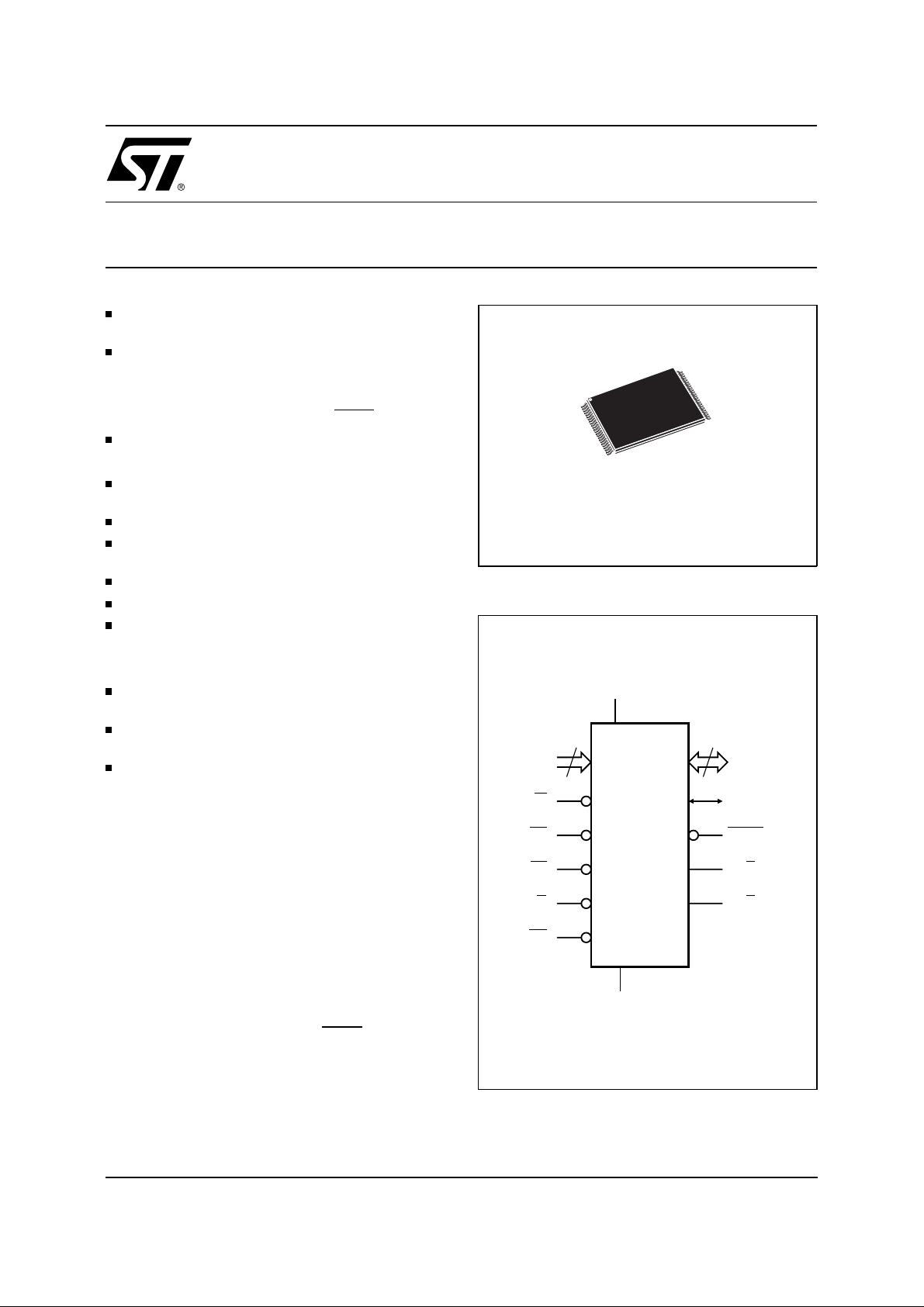
Single Chip 8 Mbit (1Mb x8 or 512Kb x16) Flash and
256 Kbit Parallel EEPROM Memory
2.7V to 3.6V SUPPLY VOLTAGE for
PROGRAM, ERASE and READ OPARATIONS
FLASH ARR A Y
– Boot block (Top or Bottom location)
– Parameter and Main blocks
– Selectable x8/x16 Data Bus (
EEPROM ARRAY
– x8 Data Bus only.
120ns ACCESS TIME
(Flash and EEPROM array)
WRITE, PROGRAM and ERASE STATUS BITS
CONCURRENT MODE (Read Flash while
writing to EEPROM)
100,000 ERASE/WRITE CYCLES
10 YEARS DA TA RETE NT ION
LOW POWER CONSUMPTION
– Stand-by mode: 100µA
– Automatic Stand-by mode
64 bytes ONE TIME PROGRAMMABLE
MEMORY (x8 Data Bus only)
ST A NDA RD EPRO M /OTP MEMORY
P ACKAGE
EXTENDED TEMPERATURE RANGES
BYTE pin).
TSOP48 (NE)
12 x 20 mm
Figure 1. Logic Diagram
V
CC
19
A0-A18
M39832
PRELIMINARY DATA
15
DQ0-DQ14
DESCRIPTION
The M39832 is a memory device combining Flash
and EEPROM into a single chip and using single
supply voltage. The memory is mapped in two
arrays: 8 Mbit of Flash memory and 256 Kbit of
W
EE
EF
M39832
G
DQ15A–1
BYTE
ERB
FRB
EEPROM memory. Each space is independant for
writing, in concurrent mode the Flash Memory can
RP
be read while the EEPROM is being written.
An additional 64 bytes of EPROM are One Time
Programmable.
The M39832 EEPROM memory array is organized
in byte only (regardless on the
BYTE pin). It may
V
SS
AI00844
be written by byte or by page of 64 bytes and the
integrity of the data can be secured with the help
of the Software Data Protection (SDP).
February 1999 1/36
This is preliminary information on a new product now in development or undergoing evaluation. Details are subject to change with out not i ce.
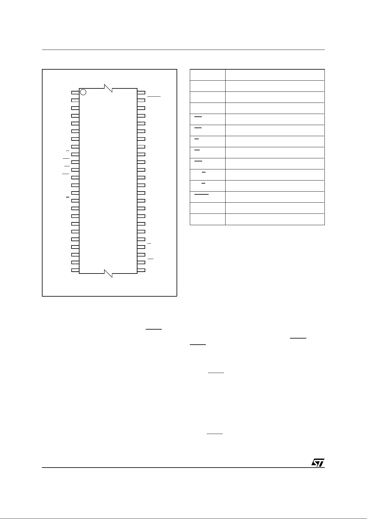
M39832
Figure 2. TSOP Pin Connections
A15
A14
A13
A12
A11
A10
ERB DQ5
EE
RP
NC
NC
FRB
A18
A17
Warning:
DESCRIPTION
1
A9
A8 DQ13
W
12
M39832
13
A7
A6
A5 DQ0
A4 G
A3
A2
24 25
A1
NC = Not Connected.
(cont’d)
48
37
36
AI00845
A16
BYTE
V
SS
DQ15A–1
DQ7
DQ14
DQ6
DQ12
DQ4
V
CC
DQ11
DQ3
DQ10
DQ2
DQ9
DQ1
DQ8
V
SS
EF
A0
The M39832 Flash Memory array can be configured as 1Mb x8 or 512Kb x16 with the
BYTE input
pin. The M39832-T and M39832-B feature asymetrically blocked architecture providing system memory integration. Both M39832-B and M39832-T
devices have a Flash array of 19 blocks, one Boot
Block of 16 KBytes or 8 KWords, two Parameter
Blocks of 8 KBytes or 4 KWords, one Main Block
of 32 KBytes or 16 KW ords and fifteen Main Blocks
of 64 KBytes or 32 KWords. The M39832-T has the
Boot Block at the top of the memory address space
and the M39832-B locates the Boot Block starting
at the bottom. The memory maps are showed in
Figures 3A and 3B. Each block can be erased
separately ,any combination of blocks can be specified for multi-block erase or the entire chip may be
erased. The Erase operations are managed automatically. The block erase operation can be sus-
Tabl e 1. Signal Names
A0-A18 Address Inputs
DQ0-DQ7 Data Input/Outputs, Commands Input
DQ8-DQ14 Data Input/Outputs
DQ15A–1 Data Input/Outputs or Address Input
EE EEPROM Array Enable
EF Flash Array Enable
G Output Enable
W Write Enable
RP Reset/Block Temporary Unprotect
ER
B EEPROM Ready/Busy Output
B Flash Ready/Busy Output
FR
BYTE Flash Array Byte/Word Organization
V
CC
V
SS
Supply Voltage
Ground
pended in order to read from or program to any
block not being ersased, and then resumed. Block
protection provides additional data security. Each
block can be separately protected or unprotected
against Program or Erase on programming equipment. All previously protected blocks can be temporarily unprotected in the applic ation. The Flash
memory array is functionally compatible with the
M29W800 Single Voltage Flash Memory device.
During a Program or Erase cycle in the F lash array
or during a Write in the EE PR OM ar ray, status bits
available on certain DQn pins provide information
on the M39832 internal logic.
PIN DESCRIPTION
. The
Byte/Word Organization Select (
BYTE)
BYTE input selects the output configuration for the
Flash array: Byte-wide (x8) mode or Word-wide
(x16) mode. The EEPROM array and the 64 Bytes
OTP Row are always accessed Byte-wide (x8).
BYTE is High, the Word-wide mode is se-
When
lected for the Flash array ( x16) and the data are
read and programmed on DQ0-DQ15. The Flash
array is accessed with A0-A18 Adrress lines. In this
mode, data in the EEPROM array (x8) are read and
programmed on DQ0-DQ7 and the array is accessed with A0-A14. The 64 bytes OTP are read
and programmed on DQ0-DQ7 and are accessed
with A0-A5 and A6 = 0.
BYTE is Low , the Byte-wide mode is selected
When
for the Flash array (x8) and the data are read and
2/36

M39832
Table 2. Absolute Maximum Ratings
Symbol Parameter Value Unit
T
A
T
BIAS
T
STG
(2)
V
IO
V
CC
, VG, V
V
A9
Notes:
EF
1. Except for the rating "Operating Temperature Range", stresses above those listed in the Table "Absolute Maximum Ratings"
may cause permanent damage to the device. These are stress ratings only and operation of the device at these or any other
conditions above those indicated in the Operating sections of this specification is not implied. Exposure to Absolute Maximum
Rating conditions for extended periods may affect device reliability. Refer also to t he STMicroelectroni cs SURE Pro gr am and other
relevant quality documents.
2. Minimum Voltage may undershoot to –2V during transition and for less than 20ns.
Ambient Operating Temperature –40 to 85
Temperature Under Bias –50 to 125
Storage Temperature –65 to 150
Input or Output Voltages –0.6 to 5 V
Supply Voltage –0.6 to 5 V
(2)
A9, G, EF Voltage –0.6 to 13.5 V
programmed on DQ0-DQ7. In this mode, DQ8DQ14 are at high impedance and DQ15A–1 is the
LSB address bit, making the Flash array to be
accessed with A–1-A18 Adress lines. In this mode,
data in the EEPROM array (x8) are read and
programmed on DQ0-DQ7 and the array is accessed with A–1-A13. The 64 bytes OTP are read
and programmed on DQ0-DQ7 and are accessed
with A-1 - A4 and A6 = 0.
Address Inputs (A0-A18).
The address inputs for
the memory array are latched during a write operation on the falling edge at Chip Enable (
or Write Enable
W. In Word-wide organisation the
address lines are A0-A18, in Byte-wide organisation DQ15A–1 acts as an additional LSB address
line. When A9 is raised to V
ID
Electronic Signature Manufacturer or Device Code,
Block Protection Status or a Write Block Protection
or Block Unprotection is enabled depending on the
combination of levels on A0, A1, A6, A12 and A15.
Data Input/Output (DQ0-DQ7).
puts/Outputs are used in the Byte-wide and Wordwide organisations. The input is data to be
programmed in the memory array or a comma nd
to be written. Both are latched on the rising edge
of Chip Enable (
EE or EF) or Write Enable W. The
output is data from the Memory Array, the Electronic Signature Manufacturer or Device codes, the
Block Protection Status or t he S tatus r egister Data
Polling bit DQ7, the T oggle Bits DQ6 and DQ2, the
Error bit DQ5 or the Erase Timer bit DQ3. Outputs
are valid when Chip Enable (
Enable
G are active. The output is high impedance
EE or EF) and Output
when the chip is deselected or the outputs are
disabled and when
RP is at a Low level.
Data Input/Outputs ( DQ8-DQ14 and DQ15A–1).
(1)
EE or EF)
, either a Read
These In-
DQ14 and DQ15A–1 act as the MSB of the Data
Input or Output, functioning as described for DQ0DQ7 above, and DQ8 - DQ15 are ’don’t care’ for
command inputs or status outputs. When
Low , DQ8-DQ14 are high impedance, DQ15A–1 is
the Address A–1 input.
Memory Array En able (
Array Enable (
EE or EF) activates the memory
EE and EF).
control logic, input buffers, decoders and sense
amplifiers. When the
EE input is driven high, the
EEPROM memory array is not selected; when the
EF input is driven high, the Flash memory array is
not selected. Attempts to access both EEPROM
and Flash arrays (
EE low and EF low) are forbidden. Switching between the two memory array
enables (
EE and EF) must not be made on the
same clock cycle, a delay of greater than t
be inserted.
The M39832 is in standby when both
are High (when no internal Erase or programming
is running). The power consumption is reduced to
the standby level and the outputs are in the high
impedance state, independent of the Output En-
G or Write Enable W inputs.
able
After 150ns of inactivity and when the addresses
are driven at CMOS levels, the chip automatically
enters a pseudo standby mode where consumption
is reduced to the CMOS standby value, while the
outputs continue to drive the bus.
The Output Enable gates the
Output Enable (
G).
outputs through the data buffers during a read
operation. The data outputs are in the high impedance state when the Output Enable
During Block Protect and Block Unprotect operations, the
G input must be forced to VID level (12V
+ 0.5V) (for Flash memory array only).
These Inputs/Outputs are additionally used in the
Word-wide organisation. W hen
BYTE is High DQ8-
C
°
C
°
C
°
BYTE is
The Memory
must
EHFL
EF and EE
G is High.
3/36
M39832
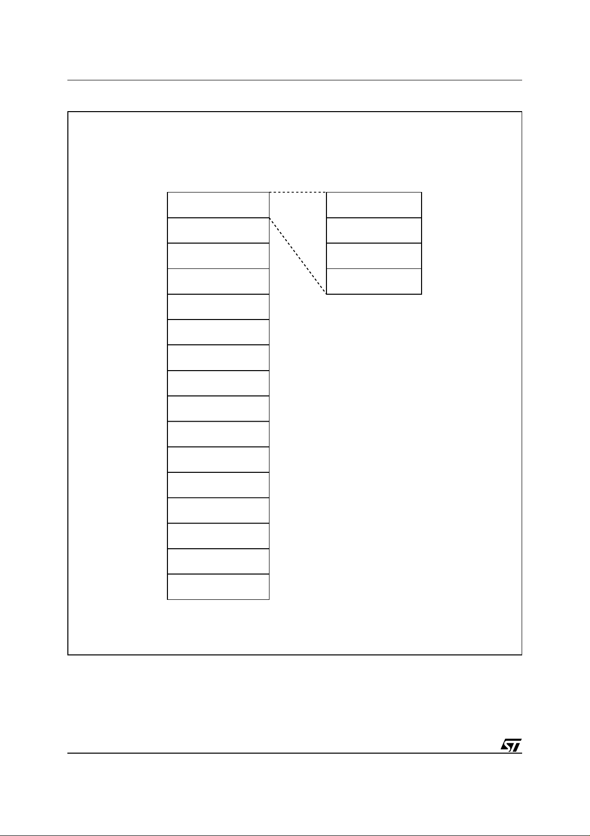
Figure 3A. Top Boot Block Memory Map and Block Address Table
TOP BOOT BLOCK
7FFFFh
78000h
77FFFh
70000h
6FFFFh
68000h
67FFFh
60000h
5FFFFh
58000h
57FFFh
50000h
4FFFFh
48000h
47FFFh
40000h
3FFFFh
38000h
37FFFh
30000h
2FFFFh
28000h
27FFFh
20000h
1FFFFh
18000h
17FFFh
10000h
0FFFFh
08000h
07FFFh
00000h
Byte-WideWord-Wide
FFFFFh
F0000h
EFFFFh
E0000h
DFFFFh
D0000h
CFFFFh
C0000h
BFFFFh
B0000h
AFFFFh
A0000h
9FFFFh
90000h
8FFFFh
80000h
7FFFFh
70000h
6FFFFh
60000h
5FFFFh
50000h
4FFFFh
40000h
3FFFFh
30000h
2FFFFh
20000h
1FFFFh
10000h
0FFFFh
00000h
64K MAIN BLOCK
64K MAIN BLOCK
64K MAIN BLOCK
64K MAIN BLOCK
64K MAIN BLOCK
64K MAIN BLOCK
64K MAIN BLOCK
64K MAIN BLOCK
64K MAIN BLOCK
64K MAIN BLOCK
64K MAIN BLOCK
64K MAIN BLOCK
64K MAIN BLOCK
64K MAIN BLOCK
64K MAIN BLOCK
16K BOOT BLOCK
8K PARAMETER BLOCK
8K PARAMETER BLOCK
32K MAIN BLOCK
AI01725B
Byte-Wide Word-Wide
FFFFFh
FC000h
FBFFFh
FA000h
F9FFFh
F8000h
F7FFFh
F0000h
7FFFFh
7E000h
7DFFFh
7D000h
7CFFFh
7C000h
7BFFFh
78000h
4/36
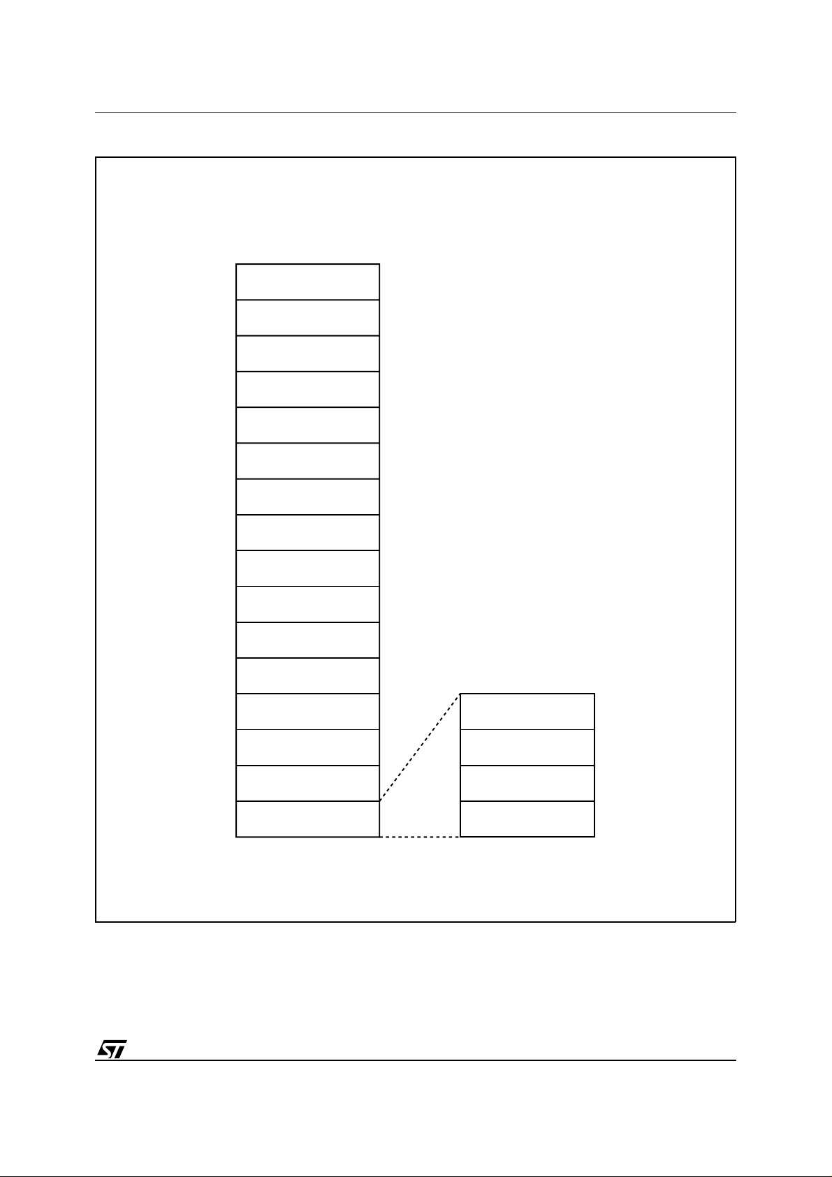
Figure 3B. Bottom Boot Block Memory Map and Block Address T able
BOTTOM BOOT BLOCK
Byte-WideWord-Wide
FFFFFh
78000h
77FFFh
70000h
6FFFFh
68000h
67FFFh
60000h
5FFFFh
58000h
57FFFh
50000h
4FFFFh
48000h
47FFFh
40000h
3FFFFh
38000h
37FFFh
30000h
2FFFFh
28000h
27FFFh
20000h
1FFFFh
18000h
17FFFh
10000h
0FFFFh
08000h
07FFFh
00000h
FFFFFh7FFFFh
F0000h
EFFFFh
E0000h
DFFFFh
D0000h
CFFFFh
C0000h
BFFFFh
B0000h
AFFFFh
A0000h
9FFFFh
90000h
8FFFFh
80000h
7FFFFh
70000h
6FFFFh
60000h
5FFFFh
50000h
4FFFFh
40000h
3FFFFh
30000h
2FFFFh
20000h
1FFFFh
10000h
0FFFFh
00000h
64K MAIN BLOCK
64K MAIN BLOCK
64K MAIN BLOCK
64K MAIN BLOCK
64K MAIN BLOCK
64K MAIN BLOCK
64K MAIN BLOCK
64K MAIN BLOCK
64K MAIN BLOCK
64K MAIN BLOCK
64K MAIN BLOCK
64K MAIN BLOCK
64K MAIN BLOCK
64K MAIN BLOCK
64K MAIN BLOCK
32K MAIN BLOCK
8K PARAMETER BLOCK
8K PARAMETER BLOCK
16K BOOT BLOCK
M39832
Byte-Wide Word-Wide
0FFFFh
08000h
07FFFh
06000h
05FFFh
04000h
03FFFh
00000h
07FFFh
04000h
03FFFh
03000h
02FFFh
02000h
01FFFh
00000h
AI01731B
5/36
M39832
T ab le 3A. M39832-T Block Address T ab le
Address Range (x8) Address Range (x16) A18 A17 A16 A15 A14 A13 A12
00000h-0FFFFh 00000h-07FFFh 0000XXX
10000h-1FFFFh 08000h-0FFFFh 0001XXX
20000h-2FFFFh 10000h-17FFFh 0010XXX
30000h-3FFFFh 18000h-1FFFFh 0011XXX
40000h-4FFFFh 20000h-27FFFh 0100XXX
50000h-5FFFFh 28000h-2FFFFh 0101XXX
60000h-6FFFFh 30000h-37FFFh 0110XXX
70000h-7FFFFh 38000h-3FFFFh 0111XXX
80000h-8FFFFh 40000h-47FFFh 1000XXX
90000h-9FFFFh 48000h-4FFFFh 1001XXX
A0000h-AFFFFh 50000h-57FFFh 1010XXX
B0000h-BFFFFh 58000h-5FFFFh 1111XXX
C0000h-CFFFFh 60000h-67FFFh 1100XXX
D0000h-DFFFFh 68000h-6FFFFh 1101XXX
E0000h-EFFFFh 70000h-77FFFh 1110XXX
F0000h-F7FFFh 78000h-7BFFFh 11110XX
F8000h-F9FFFh 7C000h-7CFFFh 1111100
FA000h-FBFFFh 7D000h-7DFFFh 1111101
FC000h-FFFFFh 7E000h-7FFFFh 111111X
6/36
M39832
T ab le 3B. M39832-B Block Address Table
Address Range (x8) Address Range (x16) A18 A17 A16 A15 A14 A13 A12
00000h-03FFFh 00000h-01FFFh 0 0 0 0 0 0 X
04000h-05FFFh 02000h-02FFFh 0 0 0 0010
06000h-07FFFh 03000h-03FFFh 0 0 0 0011
08000h-0FFFFh 04000h-07FFFh 0 0 0 0 1 X X
10000h-1FFFFh 08000h-0FFFFh 0 0 0 1 X X X
20000h-2FFFFh 10000h-17FFFh 0 0 1 0 X X X
30000h-3FFFFh 18000h-1FFFFh 0 0 1 1 X X X
40000h-4FFFFh 20000h-27FFFh 0 1 0 0 X X X
50000h-5FFFFh 28000h-2FFFFh 0 1 0 1 X X X
60000h-6FFFFh 30000h-37FFFh 0 1 1 0 X X X
70000h-7FFFFh 38000h-3FFFFh 0 1 1 1 X X X
80000h-8FFFFh 40000h-47FFFh 1 0 0 0 X X X
90000h-9FFFFh 48000h-4FFFFh 1 0 0 1 X X X
A0000h-AFFFFh 50000h-57FFFh 1 0 1 0 X X X
B0000h-BFFFFh 58000h-5FFFFh 1 0 1 1 X X X
C0000h-CFFFFh 60000h-67FFFh 1 1 0 0 X X X
D0000h-DFFFFh 68000h-6FFFFh 1 1 0 1 X X X
E0000h-EFFFFh 70000h-77FFFh 1 1 1 0 X X X
F0000h-FfFFFh 78000h-7FFFFh 1 1 1 1 X X X
7/36
M39832
Table 4. Basic Operations
EF EE G W Operation
V
IL
V
IH
V
IL
V
IH
V
IL
V
IH
V
IH
Note:
X = V
or VIH.
IL
Write Enable (
falling edge of
the rising edge of
W).
W, and Data Inputs are latched on
W.
EEPROM Ready/Busy (ER
V
IH
V
IL
V
IH
V
IL
V
IH
V
IL
V
IH
V
IL
V
IL
V
IH
V
IH
V
IH
V
IH
X X Standby, DQn = Hi-Z
Addresses are latched on the
The EEPROM
B).
Ready/Busy pin outputs the status of the device
when the EEPROM memory array is under the
write condition
B = ’0’: internal writing is in process,
–ER
B = ’1’: no internal writing in in process.
–ER
This status pin can be used when reading (or
fetching opcodes) in the Flash memory array.
The EEPROM Ready/Busy output uses an open
drain transistor, allowing therefore the use of t he
M39832 in multi-memory applications with all
Ready/Busy outputs connected to a single
Ready/Busy line (OR-wired with an external pull-up
resistor).
Flash Ready/Busy is an
Flash Ready/Busy (FR
B).
open-drain output and gives the internal state of
Flash array. When FR
B is Low, the Flash array is
Busy with a Program or Erase operation and it will
not accept any additional program or erase instructions except the Erase Suspend instruction. When
B is High, the Flash array is ready for any Read,
FR
Program or Erase operation. The FR
B will also be
High when the Flash array is put in E rase Sus pend
or Standby modes.
Reset/Block Temporary Unprotect Input (
RP Input provides hardware reset of the Flash
The
RP)
array and temporary unprotection of the protected
Flash block(s). Reset of the Flash array is
acheived by pulling
RP to VIL for at least t
PLPX
When the reset pulse is given while the Flash array
is in Read or Standby modes, it will be available for
new operations in t
after the rising edge of RP.
PHEL
If the Flash array is in Erase, Erase Suspend or
Program modes the reset will take t
PLYH
during
V
IH
V
IH
V
IL
V
IL
V
IH
V
IH
which the FR
Read in Flash Array
Read in EEPROM Array
Write in Flash Array
Write in EEPROM Array
Output Disable, DQn = Hi-Z
Output Disable, DQn = Hi-Z
B signal will be held at VIL. The end
of the Flash array reset will be indicated by the
rising edge of FR
B. A hardware reset during an
Erase or Program operation will corrupt the data
being programmed or the block(s) being erased.
See T able 14 and Figure 9. Temporary block unprotection is made by holding
RP at VID. In this condition, previously protected blocks can be
programmed or erased. The transition of
to VID must be slower than t
V
IH
15 and Figure 9. When
all blocks temporarily unprotected will be again
V
IH
RP is returned from VID to
PHPHH
protected.
OPERATIONS
An operation is defined as the basic decoding of
the logic level applied to the control input pins (
EE, G, W) and the specified voltages applied on
the relevant address pins. These operations are
detailed in Table 3.
Both Chip Enable and Output Enable (that
Read.
EF and G or EE and G) must be low in order to
is
read the output of the memory.
Read operations are used to output the contents
from the Flash or EEPROM array, the Manufacturer
identifier, the Flash Block protection Status, the
Flash Identifier, the EEPROM identifier or the OTP
row content.
.
Notes:
– The Chip Enable input mainly provides power
.
control and should be used for device selection.
The Output Enable input should be used to gate
data onto the output in combination with active
EF or EE input signals.
– The data read depends on the previous instruc-
tion entered into the memory.
RP from
. See Table
EF,
8/36
T ab le 5A. Flash Instructions (EF=0, EE=1)
M39832
Mne. Instr. Cyc.
RD
Memory
Read/Reset
(2,4)
Array
(4)
AS
Auto Select 3+
PG Program 4
BE Block Erase 6
1+
3+
Addr.
Data
Addr.
(3,7)
Data
Addr.
(3,7)
Data
Addr.
(3,7)
Data
Addr.
(3,7)
(3,7)
Byte
Word
Byte
Word
Byte
Word
Byte
Word
1st
Cyc.
X
2nd
Cyc.
3rd
Cyc.
4th
Cyc.
5th
Cyc.
Read Memory Array until a new write cycle is initiated.
F0h
AAAAh 5555h AAAAh
Read Memory Array until a new write
5555h 2AAAh 5555h
cycle is initiated.
AAh 55h F0h
AAAAh 5555h AAAAh
5555h 2AAAh 5555h
Read Electronic Signature or Block
Protection Status until a new write
cycle is initiated. See Note 5 and 6.
AAh 55h 90h
AAAAh 5555h AAAAh Program
5555h 2AAAh 5555h
Address
Read Data Polling or
Toggle Bit until Program
completes.
AAh 55h A0h
Program
Data
AAAAh 5555h AAAAh AAAAh 5555h
5555h 2AAAh 5555h 5555h 2AAAh
6th
Cyc.
Block
Address
7th
Cyc.
Additiona
l Block
(8)
Data
Byte
Word
FAE
Flash Array
Erase
Addr.
(3,7)
6
Data
(3,7)
Addr.
Data
Addr.
Data
(3,7)
will output Manufacturer code (20h). Address bits A0 at VIH and A1, at VIL will output
IL
, A1 at VIH and A15-A18 within the Block will output the Bl ock P rot ect ion st atus .
IL
B until Erase completes.
Erase
(10)
ES
Notes:
Suspend
Erase
ER
Resume
1. Commands not interpreted in this table will default to read array mode.
2. A wait of t
before starting any new operation (see Table 14 and Figure 9).
3. X = Don’t Care.
4. The first cycles of the RD or AS instructions are followed by read operations. Any number of read cycles can occur after
the command cycles.
5. Signature Address bits A0, A1, at V
Flash code.
6. Block Protection Address: A0, at V
7. For Coded cycles address inputs A11-A18 are don’t care.
8. Optional, additional Blocks addresses must be entered within the erase timeout delay after last write entry, timeout status
can be verified through DQ3 value (see Erase Timer Bit DQ3 description). When full comma nd is entered, read Data Polling
or Toggle bi t until Eras e is comp le ted or suspended.
9. Read Data Polling, Toggle bits or FR
10.During Erase Suspend, Read and Data Program functions are allowed in blocks not being erased.
PLYH
1
1
is necessary after a Read/Reset command if the memory was in an Erase or Program mode
AAh 55h 80h AAh 55h 30h 30h
AAAAh 5555h AAAAh AAAAh 5555h AAAAh
5555h 2AAAh 5555h 5555h 2AAAh 5555h
AAh 55h 80h AAh 55h 10h
X
Read until Toggle stops, then read all the data needed
from any Block(s) not being erased then Resume Erase.
B0h
X
Read Data Polling or Toggle Bits until Erase completes
or Erase is suspended another time
30h
Note 9
9/36
M39832
T able 5B. EEPROM Instructions (EE=0, EF=1)
Mne. Instr. Cyc.
Byte 5555h 2AAAh
Word
WOTP
(2)
Write OTP
Row
>3
Addr.
Data
Byte 5555h 2AAAh
Word
ROTP
(2)
Read OTP
Row
>3
Addr.
Data
RT
SSDP
Return
from OTP
Read
(4)
SDP Enable≥3
Addr.
1
Data
Addr.
Byte
Word
Data
Byte
Word
SSDP
(5)
SDP
Disable
Addr.
6
Data
Notes:
1. X = Don’t Care.
2. Once the WOTP has been initiated (first 3 Cycles), from 1 up to 64 bytes can be written in one single write cycle
(See Write OTP chapter in following pages).
3. Once the ROTP has been initiated (first 3 Cycles), from 1 up to 64 bytes of the OTP can be read (See Read OTP chapter
in following pages). The RT (Return) instruction MUST be sent to the device to exit ROTP mode.
4. Once SDP is set (SSDP instruction sent once), it is necessary to send SSDP prior to any byte or page to be written
in the EEPROM array (See Figure 4 and EEPROM array Software Data Protection chapter in following pages).
5. See Figure 5 and EEPROM array Software Data Protection chapter in following pages.
1st
Cyc.
5555h
AAh 55h B0h Byte 1
5555h
AAh 55h 90h Byte 1
X
F0h
5555h 2AAAh 5555h
5555h 2AAAh 5555h
AAh 55h A0h
5555h 2AAAh 5555h 5555h 2AAAh 5555h
5555h 2AAAh 5555h 5555h 2AAAh 5555h
AAh 55h 80h AAh 55h 20h
2nd
Cyc.
2AAAh 5555h
2AAAh 5555h
(1)
3rd
Cyc.
5555h
4th
Cyc.
5th
Cyc.
Addr 1 Addr 2 Addr 3 Addr 4
Byte 2 Byte 3 Byte 4
5555h Addr 1 Addr 2 Addr 3 Addr 4
Byte 2 Byte 3 Byte 4
6th
Cyc.
7th
Cyc.
10/36
M39832
T ab le 6. User Bus Operations
(1)
Operation EE EF G W RP BYTE A0 A1 A6 A9 A12 A15
Block
Protection
(2,4)
Blocks
Unprotection
V
IH
VILV
V
IH
(4)
VIDV
V
IL
V
ID
Pulse
V
IL
ID
Pulse
X XXXVIDXX X X X
IH
V
X XXXVIDVIHV
IH
Block
V
Protection
(2,4)
Verify
Block
Unprotection
(2,4)
Verify
Block
Temporary
IH
VILVILV
V
IH
VILVILV
V
IH
XX X VIDX XXXX X X X X X
IHVIH
IHVIH
XVILVIHVILVIDA12 A15 X X
XVILVIHVIHVIDA12 A15 X X
Unprotection
V
VILVIHVILA0 A1 VILVIDXXA–1 X
Write the
EEPROM
Identifier
(5)
V
IL
Read the
V
EEPROM
Identifier
Notes:
(5)
1. X = V
2. Block Address must be given on A12-A18 bits.
3. See Table 8.
4. Operation performed on programming equipment.
5. The 65 Bytes User defined EEPROM Identifier are accessed on DQ0-DQ7 with A0 to A5 when
when
IL
or V
IL
IH
BYTE = 0 (x8)
V
V
IH
IH
IH
VILVIHVIHA0 A1 VILVIDXX X X
V
IH
VILV
V
IL
IHVIHVIL
V
IHVIHVIH
A0 A1 VILVIDXXA–1 X
A0 A1 VILVIDXX X X
DQ15
A–1
IH
DQ8-
DQ14
XX X
BYTE = 1 (x16) or with A–1 to A4
DQ0-DQ7
Block Protect
Block Protect
Status
Status
(3)
(3)
64 Bytes User
Defined
64 Bytes User
Defined
64 Bytes User
Defined
64 Bytes User
Defined
T able 7. Read Electronic Signature (following AS instruction or with A9 = VID)
Org. Code Device EE EF G W BYTE A0 A1
Word-
wide
Manufacturer V
Flash
M39832-T V
M39832-B V
Manufacturer V
IHVILVILVIH
IHVILVILVIH
IHVILVILVIH
IHVILVILVIH
V
VILV
IH
V
VIHVILDon’t Care 0 00h D7h
IH
V
VIHVILDon’t Care 0 00h 5Bh
IH
V
VILVILDon’t Care
IL
Byte-
wide
M39832-T V
IHVILVILVIH
V
VIHVILDon’t Care
IL
Flash
M39832-B V
IHVILVILVIH
V
VIHVILDon’t Care
IL
Other
Addresses
Don’t Care 0 00h 20h
IL
DQ15
A–1
Don’t
Care
Don’t
Care
Don’t
Care
DQ8-
DQ14
DQ0-
DQ7
Hi-Z 20h
Hi-Z D7h
Hi-Z 5Bh
11/36
 Loading...