

Single Chip 4 Mbit Flash Memory and
■ Multiple Memories on a Single Chip:
– 4 Mbit Flash Memory (organised as 8 sectors)
– 256 Kbit EEPRO M
– 64 Byte One Time Programmable Memory
■ CONCURRENT Mode (Read Flash while
writing to EEPROM)
■ WRITE, PROGRAM and ERAS E Sta t u s Bits
■ 2.7V to 3.6V Single Supply Voltage for
PROGRAM, ERASE and READ Operat ions
■ 100 ns Access Time (Flash and EEPROM
blocks)
■ Low Power Consumption
–60µA Stand-by mode (maximum)
– Deep Power Down mode:
6 µA (maximum), 200 nA (typical)
■ Standard Flash Memory Package
■ 100,000 Erase/Write Cycles (minimum)
■ 10 Year Data Retention (minimum)
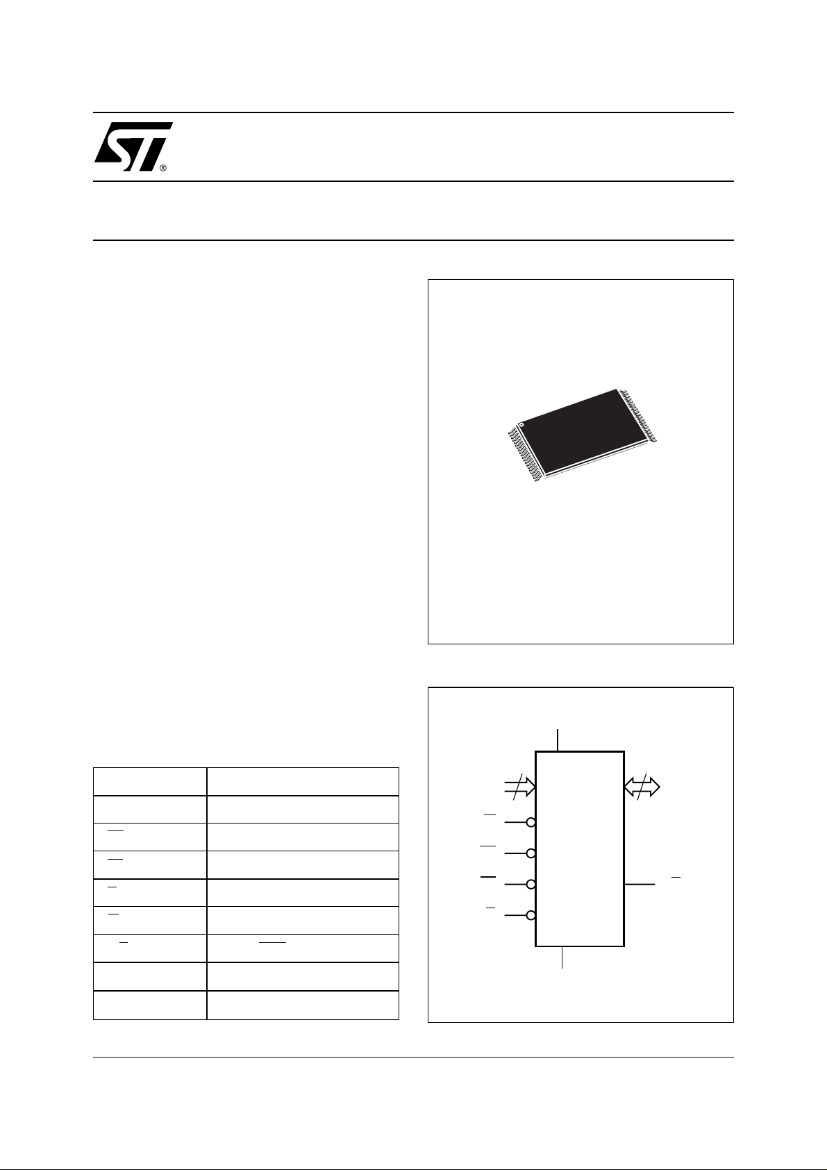
M39432
256 Kbit Parallel EEPROM
TSOP40 (NC)
10 x 20 mm
DESCRIPTION
The M39432 is a single supply voltage memory
device combining Flash memory and EEPROM on
a single chip. The memory is mapped in two
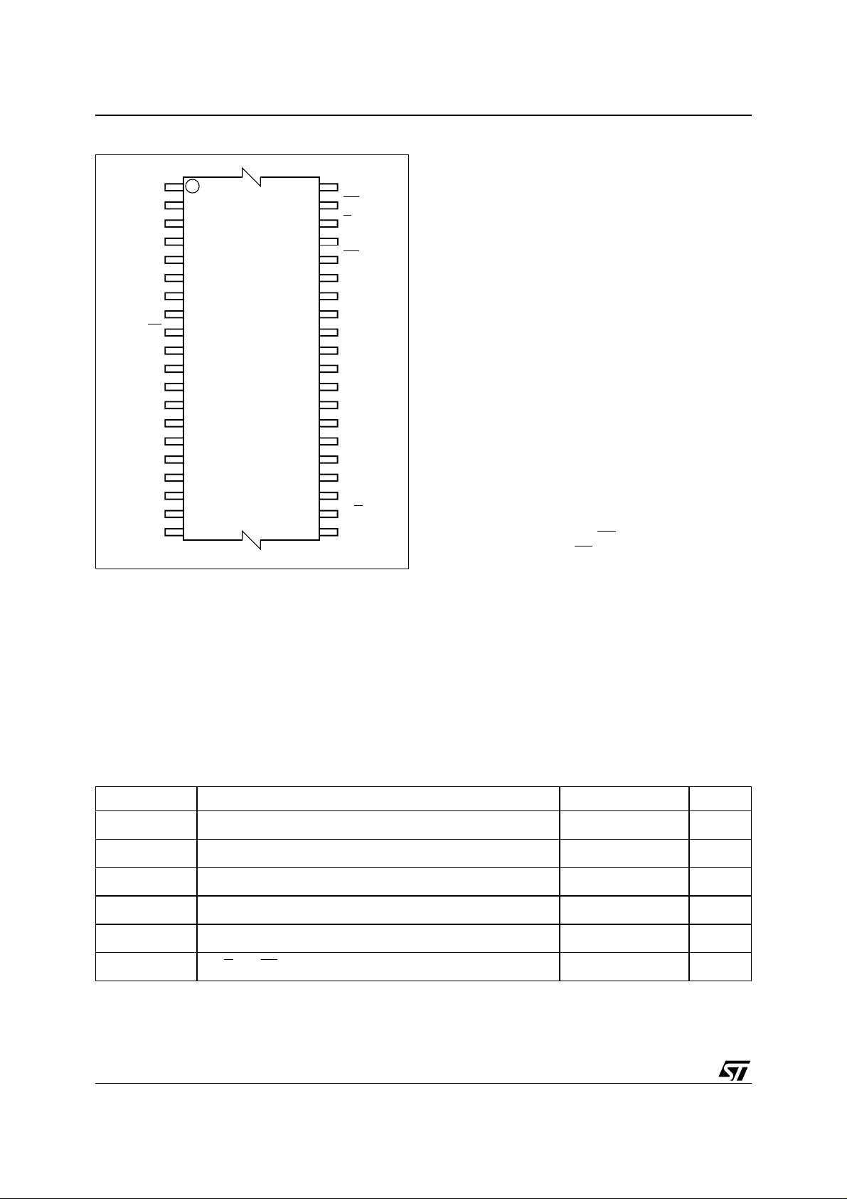
Table 1. Signal Names
A0-A18 Address Inputs
DQ0-DQ7 Data Inputs / Outputs
EE
EF
G
W
R/B
V
CC
V
SS
EEPROM Block Enable
Flash Block Enable
Output Enable
Write Enable
Ready/Busy Output
Supply Voltage
Ground
Figure 1. Logic Diagram
V
CC
19
A0-A18
W
EE
EF
G
M39432
V
SS
8
DQ0-DQ7
R/B
AI01946
1/28November 1999
M39432
Figure 2. TSOP Connection s
NC
NC
A11
A9 A10
A8 EF
A13
A14
A17
V
CC
A18
A16
A15
A12
A7
A6 A1
A5 A2
A4
NC
NC
Note: 1. NC = Not Connected.
1
W
10
11
20 21
M39432
40
31
30
AI01947
NC
EE
G
DQ7
DQ6
DQ5
DQ4
DQ3
V
SS
DQ2
DQ1
DQ0
A0
A3
R/B
NC
blocks: 4 Mbit of Flash memory and 256 Kbit of
EEPROM. Each block operates independently
during a Write cycle: in concurrent mode, the
Flash Memory can be read while the EEP ROM is
being written.
There is also a 64 byte row of OTP (one time
programmable) EPROM.
The M39432 EEPROM block may be written
bytewise or by a page at a time (up to 64 bytes).
The integrity of the data can be s ecured with the
help of the Software Data Protection (SDP).
The M39432 Flash Memory block offers 8 sectors,
each one 64 KByt e in size. Each sector may be
erased individually, and programmed a byte at a
time. Each sector can be separately protected and
unprotected against Program and Erase. Sector
erasure may be suspended, while data is read
from other sectors of the Flash memory block (or
from the EEPR O M block), and then resumed. The
Flash memory block is functionally compatible with
the M29W040 (4 Mbit Single Voltage Flash
Memory).
During a Program or Erase cycle in the Flash
memory or during a Write cycle in the EEPROM,
the status of the M39432 internal logic can be read
on the Data Output pins DQ7, DQ6, DQ5 and
DQ3.
SIGNAL DESCRIPTION
Address Inputs (A0-A18)
The address inputs for the memory array are
latched during a write operation. The EEPROM
block is selected by the E E
memory block the EF
input, and the Flash
input. A0-A14 access
locations in the EEPROM block; A0-A18 access
locations in the Flash memory block.
When V
(as specified in Table 11) is applied on
ID
the A9 address input, additional device-specific
information can be accessed:
– Read the Manufacturer identifier
– Read the Flash block identifier
– Read/Write the EEPROM block identifier
– Verify the Flash Sector Protection Status.
Table 2. Absolute Maximum Ratings
Symbol Parameter Value Unit
T
A
T
BIAS
T
STG
1,2
V
IO
1
V
CC
, VG, VEF
V
A9
Note: 1. Stresses above those listed may cause permanent damage to the device. These are stress ratings only and operation of the device
2/28
at these or any oth er conditi ons abov e those indi cated in th e Operating sections of this spec ificatio n is not imp lied. Expo sure to
Absolute Maximum Rating conditions for extended periods may affect device reliability. Please see the STMicroelectronics SURE
Program an d ot her releva nt quality documents.
2. Minimum voltage ma y undershoot to –2 V, during transiti on and for less than 20 ns.
Ambient Operating Temperature –40 to 85 °C
1
Temperature Under Bias –50 to 125 °C
1
Storage Temperature –65 to 150 °C
Input or Output Voltage (except A9) –0.6 to 7 V
Supply Voltage –0.6 to 7 V
1,2
A9, G and EF Voltage –0.6 to 13.5 V
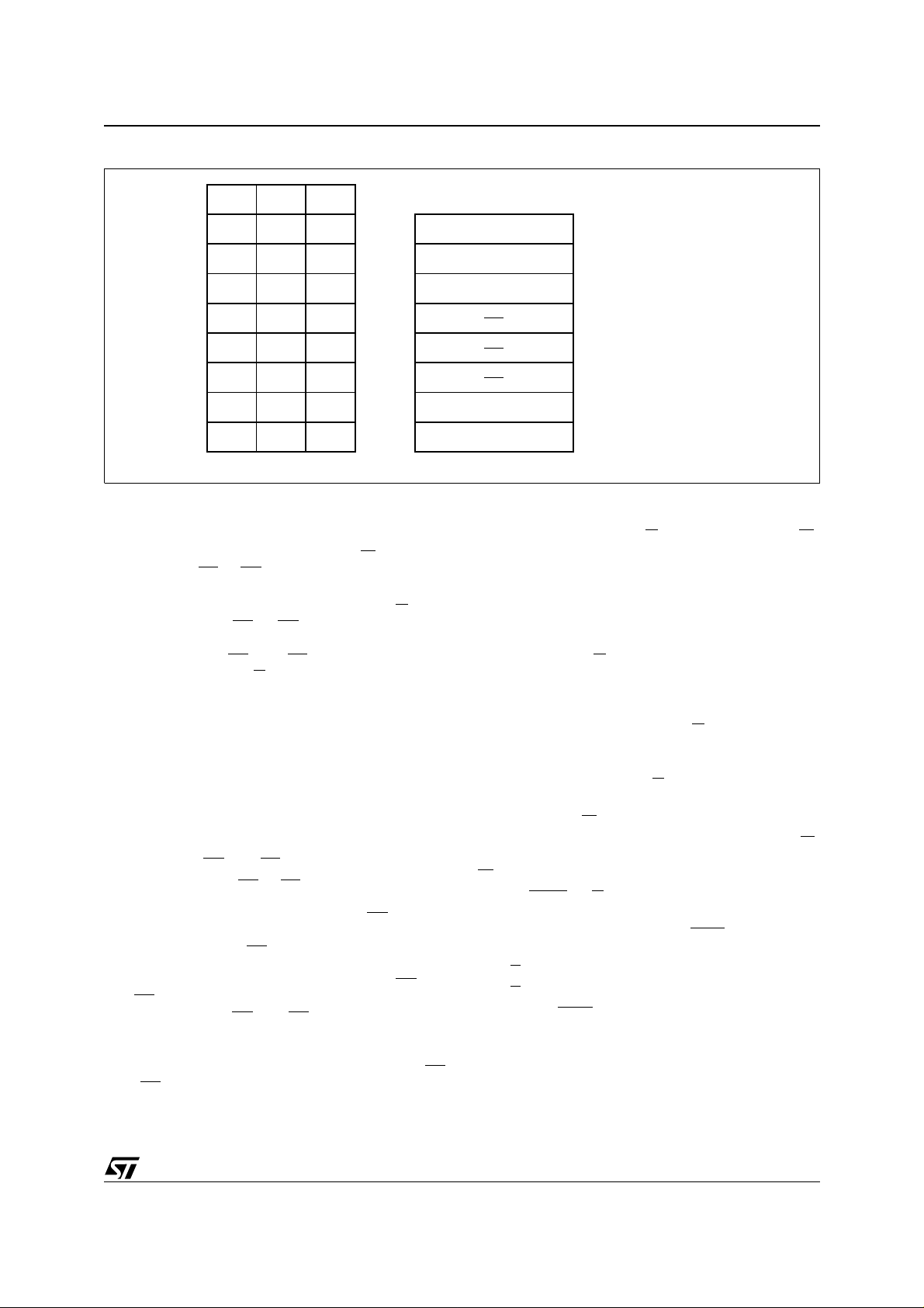
Figure 3. Flash Block Sectors
A18
A17
A16
TOP
ADDRESS
M39432
BOTTOM
ADDRESS
1
1 64K Bytes Block
1
1
0
0
001
000
AI01362B
1
1
0
0
1
1
1
0
1
0
1
0
Data Input/Output (DQ0-DQ7)
During a Write operation, one data byte is latched
into the device when Write E nable (W
Chip Enable (EF
or EE) are driven low.
) and one
During a Read operation, the output presented on
these pins is valid when Output Enable (G
one Chip Enable (E F
or EE) are driven low. The
) and
output is high impedance when the chip is
deselected (both EE
outputs are disabled (G
and EF driven high) or the
driven high).
Read operations are used to output:
– bytes in the Flash memory block
– bytes in the EEPROM block
– the Manufacturer Identifier
– the Flash Sector Protection Status
– the Flash Block Identifier
– the EEPROM Identifier
– the OTP row.
Chip Enable (EE
Each Chip Enable (EE
and EF)
or EF) causes the memory
control logic, input buffers, decoders and sense
amplifiers to be activated. When the EE
input is
driven high, the EEPROM memory block is not
selected; when the EF
input is driven high, the
Flash memory block is not sele cted. Attempts to
access both EEPROM and Flash blocks (EE
and EF
two chip enables (EE
low) are forbidden. Switching between the
and EF) must not be made
low
on the same clock cycle, a delay of greater than
must occur.
t
EHFL
The M39432 is in stand-by mode when both EF
and EE are high (when no internal Erase or
programming cycle is running). The power
consumption is reduced to the st and-by level and
64K Bytes Block
64K Bytes Block
64K Bytes Block
64K Bytes Block
7FFFFh
6FFFFh
5FFFFh
4FFFFh
3FFFFh
2FFFFh
1FFFFh
0FFFFh
70000h
60000h
50000h
40000h
30000h
20000h
10000h
00000h
the outputs are held in the high state, independent
of the Output Enable (G
) or Write Enable (W)
inputs.
After 150 ns of inactivity, and when the addresses
are driven at CMOS levels, the chip aut om atically
enters a pseudo-stand-by mode. Power
consumption is reduced to the CMOS stand-by
level, while the outputs continue to drive the bus.
Output Enable (G
)
The Output Enable gat es the outputs throug h the
data buffers during a Read operation. The data
outputs are left floating in their high impedance
state when the Output Enable (G
) is high.
During Sector Protect (Figure 8) and Sector
Unprotect (Figure 9) operations (for the Flash
memory block only), the G
(as specified in Table 11).
V
ID
Write Enable (W
)
input must be held at
Addresses are latched on the falling edge of W
and Data Inputs are latched on the rising edge of
W
.
Ready/Busy
(R/B )
When the EEPROM block is engaged in an
internal Wri te cycle, the Re ady/Busy
outp ut show s
the status of the device:
–R/B
is 0 when a Write cycle is in progress
is Hi-Z when no Write cycle is in progress
–R/B
The Ready/Busy
pin does not show the status of a
Program or Erase cycle in the Flash memory.
This pin can be used to show the status of the
EEPROM block, even when reading data (or
fetching instructions) from the Flash memory
block.
,
3/28

M39432
Table 3. Operations
Operation EF EE G W DQ0 - DQ7
Read
Write
Output Disable
Stand-by
Note: 1. X = VIH or VIL.
V
IL
V
IH
V
IL
V
IH
V
IL
V
IH
V
IH
V
IH
V
IL
V
IH
V
IL
V
IH
V
IL
V
IH
V
IL
V
IH
V
IH
X X Hi-Z
V
IH
V
IL
X Hi-Z
Read from Flash Block
Read from EEPROM Block
Write to Flash Block
Write to EEPROM Block
This open drain output can be wire-ORed, using
an external pull-up resistor, when several M39xxx
devices are used together.
Supply Voltage
V
CC
The V
Supply Voltage supplies the power for
CC
the device. The M39432 cannot be written when
the V
Voltage, V
Supply Voltage is less than the Lo ckout
CC
. This prevents Bus Write operations
LKO
from accidentally damaging the data during power
up, power down and during power surges.
A 100 nF capacitor should be connected between
the V
Supply Voltage pin and the VSS Ground
CC
pin, to decouple the current surges from the power
supply. The PCB track widths must be sufficient to
carry the currents required during program and
erase operations.
Ground
V
SS
The V
Ground is the reference for all voltage
SS
measurements.
DEVICE OPERATION
The M39432 memory d evice is addressed via 19
inputs (A0-A18) and carries data on 8 Data Inputs/
Outputs (DQ0-DQ7). There are f our other control
inputs: Chip Enable EEPROM (EE
Flash Memory (EF
Enable (W
).
), Output Enable ( E) and Write
The Chip Enable inputs (EF
), Ch ip Enab le
or EE) are used
mainly for power control (turning the chip on and
off) and for block selection (selecting the
EEPROM block or the Flash memory block). The
gating of data to the DQ0-DQ7 pins should be
controlled using the Output Enable input (G
).
The permitted operating modes of the device are
listed in Table 3.
Read
For a Read operation, the Output Enable (G
one Chip Enable (EF
or EE) must be driven low.
) and
As noted on the previous page, Read operations
are used to read the contents of:
– bytes in the Flash memory block
– bytes in the EEPROM block
– the Manufacturer Identifier
– the Flash Sector Protection Status
– the Flash Block Identifier
– the EEPROM Identifier
– the OTP row.
The instruction sequences for selecting between
these areas is summarized in Table 4.
Write
Writing data requires:
– a Chip Enable (either EE
– the Write Enable (W
Enable (G
) to be high.
or EF) to be low
) to be low and the Output
Addresses in the Flash memory block (or the
EEPROM block) are latched on the falling edge of
or EF (or E E) whichever occurs the later. The
W
data to be written to the Flash memory block (or
EEPROM block) is latched on the rising edge of W
or EF (or EE) whichever occurs first.
The Write operation is used in two contexts:
– to write data to the EEPROM memory block
– to enter the sequ ence of bytes that makes up
one of the instructions shown in Table 4.
The programming of a byte of Flash memory
involves one of these instructions (as described in
the section entitled “Instructions” on this page).
Specific Read and Write Operations
Device specific information includes the following:
– Read the Manufacturer Identifier
– Read the Device Identifier
– Define the Flash Sector Protection
– Read the EEPROM Iden tifier
– Write the EEPROM Identifier
4/28

M39432
Table 4. Instructions
1
Instruction EE EF Cycle 1 Cycle 2 Cycle 3 Cycle 4 Cycle 5 Cycle 6 Cycle 7
Read
Manufacturer
Identifier
2
Read Flash
Identifier
2
10
10
Read OTP Row 0 1
Read Sector
Protection Status
Program a Byte of
Flash Memory
Erase a Sector of
Flash Memory
Erase the Whole
of Flash Memory
Suspend Sector
Erase
Resume Sector
Erase
10
2
10
10
10
10
10
AAh
@5555h
AAh
@5555h
AAh
@5555h
AAh
@5555h
AAh
@5555h
AAh
@5555h
AAh
@5555h
B0h
@any
address
30h
@any
address
55h
@2AAAh
55h
@2AAAh
55h
@2AAAh
55h
@2AAAh
55h
@2AAAh
55h
@2AAAh
55h
@2AAAh
90h
@5555h
90h
@5555h
90h
@5555h
90h
@5555h
A0h
@5555h
80h
@5555h
80h
@5555h
Read Identifier
with (A0,A1,A6)
set to (0,0,0)
Read Identifier
with (A0,A1,A6)
set to (1,0,0)
Read
Byte 1
Read Identifier
with (A0,A1,A6)
set to (0,1,0)
Data
@ Address
AAh
@5555h
AAh
@5555h
Read
Byte 2
55h
@2AAAh
55h
@2AAAh
30h
@ Sector
address
10h
@5555h
Read
Byte N
30h
@ Sector
address
3
EEPROM Power
Down
Deep Power
Down
SDP Enable
(EEPROM)
SDP Disable
(EEPROM)
01
10
01
01
Write OTP Row 0 1
Return (from OTP
Read or
EEPROM Power
01
Down)
Reset 1 0
Reset (short
instruction)
Note: 1. AAh @ 5555h means “Write the value AAh at the address 5555h”.
2. This instruction can also be performe d as a Verify operatio n wi t h A9=V
and Unprotection” on page 18).
3. Addresses of additio nal sectors to be erased must be entered wit hi n a time- out of 80 µs of each other.
10
AAh
@5555h
20h
@5555h
AAh
@5555h
AAh
@5555h
AAh
@5555h
F0h
@any
address
AAh
@5555h
F0h
@any
address
55h
@2AAAh
55h
@2AAAh
55h
@2AAAh
55h
@2AAAh
55h
@2AAAh
30h
@5555h
A0h
@5555h
80h
@5555h
B0h
@5555h
F0h
@any
address
Write
Byte 1
AAh
@5555h
Write
Byte 1
(please see the section entitl ed “Flash Sector Prot ection
ID
Write
Byte 2
55h
@2AAAh
Write
Byte 2
Write
Byte N
20h
@5555h
Write
Byte N
5/28

M39432
Table 5. Device Identifier Operations
Instruction EF EE G W A0 A1 A6 A9
Read Manufacturer
Identifier
Read Flash Block
Identifier
Read EEPROM
Block Identifier
Note: 1. X = Don’t Care.
V
V
V
IL
V
V
IL
V
IH
V
IH
IH
IL
V
IL
V
V
IL
V
V
IL
V
IH
V
IH
IH
V
IL
IL
V
IH
XX
IL
V
IL
V
IL
V
IL
V
ID
V
ID
V
ID
Other Address
Lines
Don’t Care 20h
Don’t Care 0E3h
Don’t Care
DQ0 - DQ7
defined bytes
64 user-
To access these, A9 is held at VID (as specified in
Table 11) and the specific logic le vels, shown in
Table 5, are applied to the address input s A0, A1
and A6.
The OTP row is accessed with a specific software
sequence, as described in the section entitled
“Writing the OTP Row” on page 11.
Instructions
Instructions consist of a sequence of specific Write
operations, as summarized in Table 4. The time
between two consecutive bytes must be shorter
than the time-out value (t
WLWL
).
Each received byte i s decoded sequent ially, and
not executed as a standard Write ope ration. The
overall instruction is executed when the correct
number of bytes have been properly received.
The sequence must be followed exactly. If an
invalid combination of instruction bytes occurs, or
time-out between two consecutive bytes, the
device logic resets itself to the Read state, when
addressing the Flash block, or is di rectly de coded
as a single operation, when addressing the
EEPROM block.
The M39432 instructions set, as summarized in
Table 4, includes:
■ Program a byte in the Flash memory block
■ Read the Protection Status of a Flash Sector
■ Erase instructions:
– Flas h Secto r Er a s e
– Flash Block Erase
– Flash Sector Erase Suspend
– Flash Sector Erase Resume
■ EEPROM Power Down
■ Deep Power Down
■ Change the EEPROM software write protection:
– Enable SDP
–Disable SDP
■OTP row access:
– Write the whole OTP row (once)
– Read from the OTP row
■ Reset and Return
■ Read identifiers:
– Read the Manufacturer Identifier
– Read the Flash Block Identifier
For efficiency, each instruction consists of a twobyte escape sequence, followed by a command
byte or a confirmation byte. The escape sequence
consists of writing the value AAh at address
5555h, in the first cycle, and the value 55h at
address 2AAAh, in the second cycle.
In the case of the Erase instructions, an additional
escape sequence is required, for final confirmation
that the instruction is the intended one.
POWER SUPPLY AND CURRENT
CONSUMPTION
Power Up
The M39432 internal logic is reset, to Read mode,
upon a power-up event. All Write operations to the
EEPROM are inhibited for the first 5 ms.
No new Write cycles can be started wh en V
below V
(as specified in Table 11). Howeve r,
LKO
CC
is
for maximum security of the contents of the
memory, and to remove the possibility of a byte
being written on the first rising edge of EF
, at least one of EF, E E or W should be tied to
W
V
during the power-up process.
IH
, EE or
Stand-by
When both EE
and EF are high, the memory
enters Stand-by mode, and the Dat a In put/Ou tput
pins are placed in the high-impedan ce state. To
reduce the Supply Current to the Stand-by Supply
Current, EE
V
±0.2V.
CC
and EF should be held within
If the Stand-by mode is set during a Program or
Erase cycle, the memory continues to use the
Supply Current until the cycle is complete.
6/28
Table 6. Status Bits
EF EE DQ7 DQ6 DQ5 DQ4 DQ3 D Q2 DQ1 DQ0
Flash
EEPROM
Note: 1. X = Not a guaranteed v al ue, can be rea d ei ther as ‘1’ or ‘0 ’ .
V
IL
V
IH
V
V
Data
IH
Polling
Data
IL
Polling
Toggle
Flag
Toggle
Flag
M39432
Error
Flag
XXXXXX
Erase
X
Time-
Out
XXX
Automatic Stand-by
If CMOS le vels (V
±0.2V) are used to drive the
CC
bus, and the bus is inactive f or m ore t han 1 50 ns,
the memory enters the Automatic Stand-by state.
The internal supply current is reduced to the
Stand-by Supply Current, I
CC3
.
Deep Power Down
The I
consumption m ode can be reduced to a
CC
minimum using the Deep Power Down i nstruction
(as shown in Table 4). The device is set in a sleep
mode until the next Reset instruction is executed.
EEPROM Power Down
The M39432 can power-down the EEPROM block
using the specific instruction shown in Table 4.
Once in this state, the EEPROM block is no longer
accessible, until a Return instruction is executed.
READ
Read operations and instructions can be used:
– to read the contents of the memory array (Flash
memory block or EEPROM block)
– to read the memory array statu s and identifiers
(Flash memory block or EEPROM block).
Read Data (from Flash Memory or EEPROM)
For a Read operation, the Output Enable (G
one Chip Enable (EF
or EE) must be driven low.
) and
Read the Manufacturer Identifier
There are two alternative methods for reading the
Manufacturer Identifier: using a Read operation or
using a Read instruction.
Read Operation.
be read with a Read operation by applying V
The Manufacturer Identifier can
(as
ID
specified in Table 11) on A9, and t he logic levels
specified in Table 5 applied to A0, A1, A6.
Read Instruction.
The Manufacturer Identifier can
also be read using an instruction composed of four
operations: three specific Write operations (as
specified in Table 4) and a Re ad operation. This
either accesses the Manufacturer Identifier, the
Flash Block Identifier or the Flash Sector
Protection Status, depending on the levels that are
being applied to A0, A1, A6, A16, A17 and A18.
Read the Flash Block Identifier
Similarly, there are two alternative methods for
reading the Flash Block Identifier (E3h): using a
Read operation or using a Read instruction.
Please see the previous section, entitled “Read
the Manufacturer Identifier”, and Table 5 and
Table 4 for details.
Read the EEPROM Block Identifier
The EEPROM Block Identifier (64 bytes, user defined) can be read with a single Read operation by
holding A6 low and A9 at VID (see Table 5).
Read the OTP Row
The OTP row is mapped in the EEPROM block.
With EE
held low, and EF held high, an EEPROM
Read instruction is composed, as specified in
Figure 4. Dat a Po ll i ng F lo wc h a rt
START
READ DQ5 & DQ7
at VALID ADDRESS
DQ7
DATA
NO
DQ5
READ DQ7
DQ7
DATA
FAIL PASS
= 1
YES
=
NO
YES
YES
=
NO
AI01369B
7/28
M39432
Table 4. This consists of the writing of three
specific data bytes at three specific memory
locations (each location on a different page) as a
prefix to reading the OTP row content.
When accessing the OTP row, only the least
significant bits of the address bus (A0 to A6) are
decoded (of which A6 must be low).
Each Read of the OTP row has t o be followed by
the Return instruction (as shown in Table 4).
Read the Flash Sector Protection Status
There are two alternative methods for reading the
Flash Sector Protection Status: using a Verify
operation with A9=V
(as described on page 18)
ID
or using a Read instruction as described in the
section entitled “Read the Manufacturer Identifier”,
starting on page 7.
Using the Read instruction, the logic levels on A0,
A1, A6 select the correct instruction, while A16,
A17 and A18 specify which sector is being
addressed. This returns the value 01h if the Flash
sector is protected, and the value 0 0h if t he F lash
sector is not protected.
Read the Status Bits
The latency period of W rite, Erase and Program
cycles can be monitored by the application
software, by using the M39432 status bits. The
Ready/Busy
pin provides the status information
during a write cycle to the EEPROM block (t hough
not to the Flash memory block). An internal status
register carries the status information during a
programming or erase cycle. A Read operation,
during the program or write cycle, causes the
contents of this register to be presented to the I/O
ports (DQ0-DQ7), as summarized in Table 6.
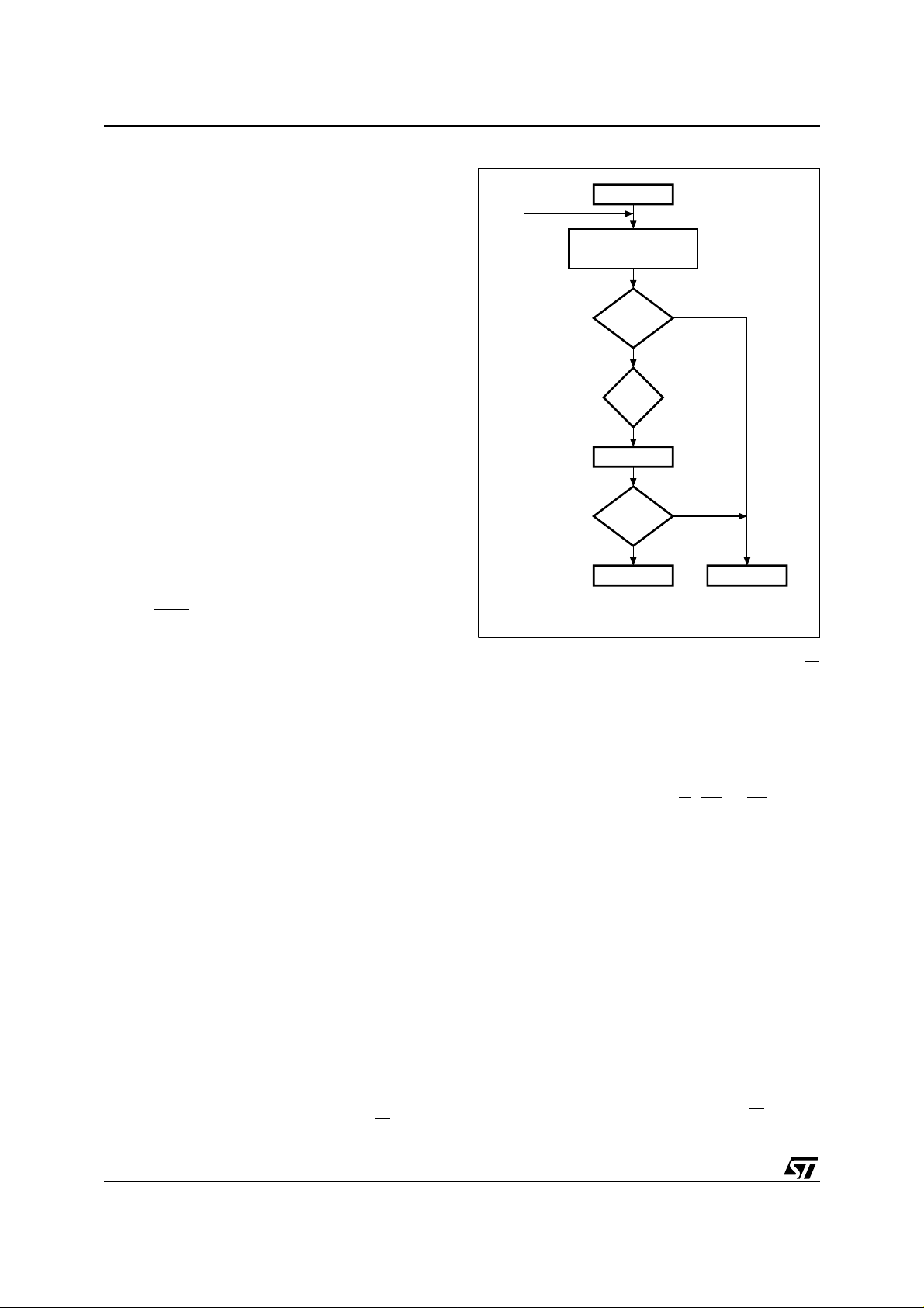
Data Polling flag, DQ7. The I/O lines (DQ0DQ7) are first used as inputs, carrying the data
that is to be written to the EEPROM or
programmed in the Flash memory. Once the Write
or Program cycle is underway, these lines become
outputs (and can be read using a normal Read
operation). The value presented on DQ7 is the
inverse of the data bit that was presented by the
user. When the cycle is complete, the lines remain
as outputs, and the value that is presented on DQ7
is the non-inverted value that was originally
specified for writing.
The suitable algorithm for using this method of
polling is shown in Figure 4. When a Write or
Program cycle is in progress, data bit DQ7 is set to
the complement of the original data bit 7 (or to ‘0’
in the case of an Erase cycle in the Flash memory
block). When DQ7 is identical to the old data (or to
‘1’ in the case of an Erase cycle in the Flash
memory block) and the Error bit (DQ5) is still ’0’,
the cycle is complete .
For the flash memory block, data Polling is
effective after the fourth pulse on the W
line for
Figure 5. Dat a Toggle Flow c hart
START
READ
DQ5 & DQ6
DQ6
=
TOGGLE
NO
DQ5
= 1
READ DQ6
DQ6
=
TOGGLE
FAIL PASS
NO
YES
YES
NO
YES
AI01370
Program cycles, and af ter the si xth pulse on th e W
line for Erase cycles. The Data Polling Read
instruction must address the same location as the
byte that is being programmed, or within the same
Flash sector as the one that is being erased.
Toggle flag , DQ6. During an internal Write,
Program or Erase cycle, DQ6 toggles between ’0’
and ’1’, on successive Read accesses to any byte
of the memory (when either G
, EE or EF is held
low).
When the internal cycle is complete, the toggling is
stopped, and the data read on DQ0-DQ7 is that of
the addressed memory byte. A subsequent
Reading at the same address will result in the
same data being read.
This alternative method for detecting when the
internal Write, Program or Erase cycle has
completed, is shown in the flowchart in Figure 5.
When an internal cycle is in progress, data bit DQ6
toggles between ‘1’ and ‘0’ for successive Read
operations. When DQ6 no longer toggles and the
Error bit DQ5 is ’0’, the operation i s complete. To
determine if DQ6 has toggled, each poll requires
two consecutive Read operations to see if the data
read is the same each time.
For the flash memory block, data Toggling is
effective after the fourth pulse on the W
line for
8/28
M39432
Table 7. Summary of the Use of Status Bits
Operation Address
DQ7 (Data
Polling Bit)
DQ6 (Toggle Bit)
Program (Flash)
or
Any address DQ7
Toggling 0 X
Erase (EEPROM)
Program Error
(Flash)
Flash Block Erase
Sector Erase
Sector Erase
before Time-Out
Any address in
the Flash block
Any address in
the Flash block
Sector address to
be erased
Sector address to
be erased
DQ7
0
0
0
Toggling 1 X
1
1
1
Toggling
Toggling
Toggling
2
2
2
Any byte in the
sector in erase
Erase Suspend
Erase Error Sector address
Note: 1. If all the sectors to be erased are protected, DQ7 is reset to 0 for about 100 µs, then returns to the state it was in for the previously
addressed byte. No erasure is perf orm ed.
2. If all the sectors to be erased are protected, DQ6 is reset to 0 for about 100 µs, then returns to the state it was in for the previously
addressed byte. No erasure is perf orm ed.
mode
Other sector
addresses
DQ6 toggles for 15 µs, then behaves as for a standard Read operaion
1
0
Invalid data on DQ7-DQ0
Toggling
2
DQ5 (Program
Error Bit)
DQ3 (Erase
Time-Out Bit)
01
01
00
11
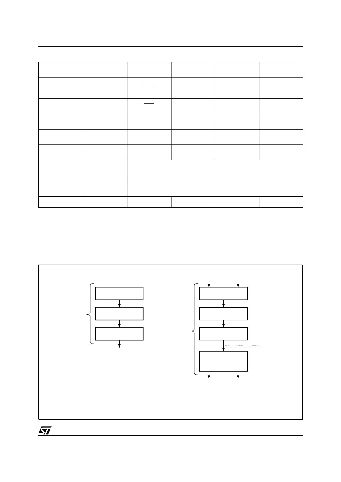
Figure 6. EEPROM SDP-Enable Flowcharts
Write AAh in
Address 5555h
Page Write
Timing
Write 55h in
Address 2AAAh
Write A0h in
Address 5555h
SDP is set
SDP ENABLE ALGORITHM
Page Write
Timing
SDP
Set
Write AAh in
Address 5555h
Write 55h in
Address 2AAAh
Write A0h in
Address 5555h
Write Data to
be Written in
any Address
Write
in Memory
SDP
not Set
Write Data
and
SDP Set
after t
WC
Write
is enabled
AI01698C
9/28
 Loading...