


64 Mbit (4Mb x16, Multiple Bank, Burst) Flash Memory
and 8 Mbit (512K x16) SRAM, Multiple Memory Product
FEATURES SUMMARY
■ SUPPLY VOLTAGE
–V
–V
–V
■ ACCESS TIME: 70, 85, 100ns
■ LOW POWER CONSUMPTION
■ ELECTRONIC SIGNATURE
– Manufacturer Code: 20h
– Top Device Code, M36WT864TF: 8810h
– Bottom Device Code, M36W T864 BF : 8811h
FLASH MEMORY
■ PROGRAMMING TIME
– 8µs by Word typical for Fast Factory Program
– Double/Quad ruple Word P rogram option
– Enhanced Factory Pro gram options
■ MEMORY BLOCKS
– Multiple Bank Memory Array: 4 Mbit Banks
– Parameter Blocks (Top or Botto m locati o n )
■ DUAL OPERATIONS
– Program Erase in one Bank while Read in
– No delay between Read and Write operations
■ BLOCK LOCKING
– All blocks locked at Power up
– Any combination of blocks can be locked
–WP
■ SECURITY
– 128 bit user programmable OTP cells
– 64 bit unique device number
– One parameter block permanent ly lockable
■ COMMON FLASH INTERFACE (CFI)
■ 100,000 PROGRAM/ERASE CYCL ES per
BLOCK
= 1.65V to 2.2V
DDF
= V
DDS
= 12V for Fast Program (optional)
PPF
= 2.7V to 3.3V
DDQF
others
for Block Lock-Down
M36WT864TF
M36WT864BF
PRODUCT PREVIEW
SRAM
■ 8 Mbit (512K x 16 bit)
■ EQUAL CYCLE and ACCESS TIMES: 70ns
■ LOW STANDBY CURRENT
■ LOW V
■ TRI-STATE COMMON I/O
■ AUTOMATIC POWER DOWN
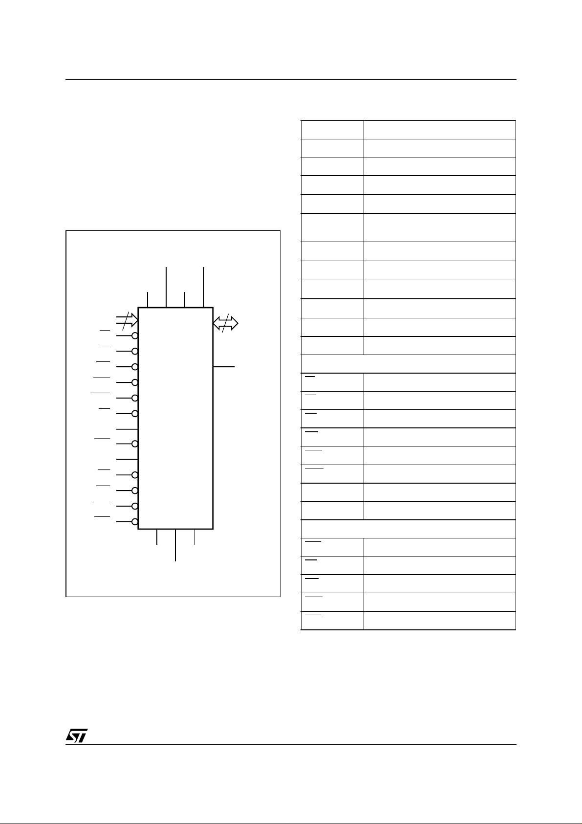
Figure 1. Packages
DATA RETENTION: 1.5V
DDS
FBGA
Stacked LFBGA96 (ZA)
8 x 14mm
July 2002
This is preliminary information on a new product now in development. Details are subject to change without notice.
1/92

M36WT864TF, M36WT864BF
TABLE OF CONTENTS
SUMMARY DESCRIPTION. . . . . . . . . . . . . . . . . . . . . . . . . . . . . . . . . . . . . . . . . . . . . . . . . . . . . . . . . . . 7
Figure 2. Logic Diagram . . . . . . . . . . . . . . . . . . . . . . . . . . . . . . . . . . . . . . . . . . . . . . . . . . . . . . . . . . 7
Table 1. Signal Names . . . . . . . . . . . . . . . . . . . . . . . . . . . . . . . . . . . . . . . . . . . . . . . . . . . . . . . . . . . 7
Figure 3. LFBGA Connections (Top view through package). . . . . . . . . . . . . . . . . . . . . . . . . . . . . . .8
SIGNAL DESCRIPTIONS . . . . . . . . . . . . . . . . . . . . . . . . . . . . . . . . . . . . . . . . . . . . . . . . . . . . . . . . . . . . 9
Address Inputs (A0-A18). . . . . . . . . . . . . . . . . . . . . . . . . . . . . . . . . . . . . . . . . . . . . . . . . . . . . . . . . . 9
Address Inputs (A19-A21). . . . . . . . . . . . . . . . . . . . . . . . . . . . . . . . . . . . . . . . . . . . . . . . . . . . . . . . . 9
Data Input/Output (DQ0-DQ15). . . . . . . . . . . . . . . . . . . . . . . . . . . . . . . . . . . . . . . . . . . . . . . . . . . . . 9
Flash Chip Enable (EF). . . . . . . . . . . . . . . . . . . . . . . . . . . . . . . . . . . . . . . . . . . . . . . . . . . . . . . . . . . 9
Flash Output Enable (GF). . . . . . . . . . . . . . . . . . . . . . . . . . . . . . . . . . . . . . . . . . . . . . . . . . . . . . . . . 9
Flash Write Enable (WF). . . . . . . . . . . . . . . . . . . . . . . . . . . . . . . . . . . . . . . . . . . . . . . . . . . . . . . . . . 9
Flash Write Protect (WPF). . . . . . . . . . . . . . . . . . . . . . . . . . . . . . . . . . . . . . . . . . . . . . . . . . . . . . . . . 9
Flash Reset (RPF). . . . . . . . . . . . . . . . . . . . . . . . . . . . . . . . . . . . . . . . . . . . . . . . . . . . . . . . . . . . . . . 9
Flash Latch Enable (LF).. . . . . . . . . . . . . . . . . . . . . . . . . . . . . . . . . . . . . . . . . . . . . . . . . . . . . . . . . . 9
Flash Clock (KF).. . . . . . . . . . . . . . . . . . . . . . . . . . . . . . . . . . . . . . . . . . . . . . . . . . . . . . . . . . . . . . . . 9
Flash Wait (WAITF). . . . . . . . . . . . . . . . . . . . . . . . . . . . . . . . . . . . . . . . . . . . . . . . . . . . . . . . . . . . . . 9
SRAM Chip Enable (E1S, E2S). . . . . . . . . . . . . . . . . . . . . . . . . . . . . . . . . . . . . . . . . . . . . . . . . . . . . 9
SRAM Write Enable (WS). . . . . . . . . . . . . . . . . . . . . . . . . . . . . . . . . . . . . . . . . . . . . . . . . . . . . . . . . 9
SRAM Output Enable (GS).. . . . . . . . . . . . . . . . . . . . . . . . . . . . . . . . . . . . . . . . . . . . . . . . . . . . . . . . 9
SRAM Upper Byte Enable (UBS). . . . . . . . . . . . . . . . . . . . . . . . . . . . . . . . . . . . . . . . . . . . . . . . . . . . 9
SRAM Lower Byte Enable (LBS). . . . . . . . . . . . . . . . . . . . . . . . . . . . . . . . . . . . . . . . . . . . . . . . . . . . 9
V
Supply Voltage. . . . . . . . . . . . . . . . . . . . . . . . . . . . . . . . . . . . . . . . . . . . . . . . . . . . . . . . . . . . . 9
DDF
V
and V
DDQF
V
Program Supply Voltage. . . . . . . . . . . . . . . . . . . . . . . . . . . . . . . . . . . . . . . . . . . . . . . . . . . . .10
PPF
V
SSF ,VSSQF
Supply Voltage. . . . . . . . . . . . . . . . . . . . . . . . . . . . . . . . . . . . . . . . . . . . . . . . . . . 10
DDS
and V
Grounds.. . . . . . . . . . . . . . . . . . . . . . . . . . . . . . . . . . . . . . . . . . . . . . . . . . . 10
SSS
FUNCTIONAL DESCRIPTION . . . . . . . . . . . . . . . . . . . . . . . . . . . . . . . . . . . . . . . . . . . . . . . . . . . . . . . 11
Figure 4. Functional Block Diagram . . . . . . . . . . . . . . . . . . . . . . . . . . . . . . . . . . . . . . . . . . . . . . . . 11
Table 2. Main Operation Modes . . . . . . . . . . . . . . . . . . . . . . . . . . . . . . . . . . . . . . . . . . . . . . . . . . . 12
Flash Memory Componen t . . . . . . . . . . . . . . . . . . . . . . . . . . . . . . . . . . . . . . . . . . . . . . . . . . . . . . . 13
SRAM Component . . . . . . . . . . . . . . . . . . . . . . . . . . . . . . . . . . . . . . . . . . . . . . . . . . . . . . . . . . . . . . 13
Table 3. Flash Bank Architecture . . . . . . . . . . . . . . . . . . . . . . . . . . . . . . . . . . . . . . . . . . . . . . . . . . 1 4
Figure 5. Flash Block Add re sse s. . . . . . . . . . . . . . . . . . . . . . . . . . . . . . . . . . . . . . . . . . . . . . . . . . . 14
FLASH BUS OPERATIONS . . . . . . . . . . . . . . . . . . . . . . . . . . . . . . . . . . . . . . . . . . . . . . . . . . . . . . . . . 15
Bus Read. . . . . . . . . . . . . . . . . . . . . . . . . . . . . . . . . . . . . . . . . . . . . . . . . . . . . . . . . . . . . . . . . . . . . 15
Bus Write. . . . . . . . . . . . . . . . . . . . . . . . . . . . . . . . . . . . . . . . . . . . . . . . . . . . . . . . . . . . . . . . . . . . . 15
Address Latch.. . . . . . . . . . . . . . . . . . . . . . . . . . . . . . . . . . . . . . . . . . . . . . . . . . . . . . . . . . . . . . . . . 15
Output Disable. . . . . . . . . . . . . . . . . . . . . . . . . . . . . . . . . . . . . . . . . . . . . . . . . . . . . . . . . . . . . . . . . 15
Standby. . . . . . . . . . . . . . . . . . . . . . . . . . . . . . . . . . . . . . . . . . . . . . . . . . . . . . . . . . . . . . . . . . . . . . 15
Reset. . . . . . . . . . . . . . . . . . . . . . . . . . . . . . . . . . . . . . . . . . . . . . . . . . . . . . . . . . . . . . . . . . . . . . . . 15
FLASH COMMAND INTERFACE. . . . . . . . . . . . . . . . . . . . . . . . . . . . . . . . . . . . . . . . . . . . . . . . . . . . .16
2/92

M36WT864TF, M36WT864BF
Table 4. Command Codes. . . . . . . . . . . . . . . . . . . . . . . . . . . . . . . . . . . . . . . . . . . . . . . . . . . . . . . . 16
COMMAND INTERFACE - STANDARD COMMANDS . . . . . . . . . . . . . . . . . . . . . . . . . . . . . . . . . 17
Read Array Command. . . . . . . . . . . . . . . . . . . . . . . . . . . . . . . . . . . . . . . . . . . . . . . . . . . . . . . . . . . 17
Read Status Register Command. . . . . . . . . . . . . . . . . . . . . . . . . . . . . . . . . . . . . . . . . . . . . . . . . . .17
Read Electronic Signature Comma nd . . . . . . . . . . . . . . . . . . . . . . . . . . . . . . . . . . . . . . . . . . . . . . . 17
Read CFI Query Command. . . . . . . . . . . . . . . . . . . . . . . . . . . . . . . . . . . . . . . . . . . . . . . . . . . . . . . 1 7
Clear Status Regist e r Command. . . . . . . . . . . . . . . . . . . . . . . . . . . . . . . . . . . . . . . . . . . . . . . . . . . 17
Block Erase Command . . . . . . . . . . . . . . . . . . . . . . . . . . . . . . . . . . . . . . . . . . . . . . . . . . . . . . . . . . 1 7
Bank Erase Command . . . . . . . . . . . . . . . . . . . . . . . . . . . . . . . . . . . . . . . . . . . . . . . . . . . . . . . . . . 1 8
Program Command. . . . . . . . . . . . . . . . . . . . . . . . . . . . . . . . . . . . . . . . . . . . . . . . . . . . . . . . . . . . . 18
Program/Erase Suspend Comm and . . . . . . . . . . . . . . . . . . . . . . . . . . . . . . . . . . . . . . . . . . . . . . . . 18
Program/Eras e Resume Command . . . . . . . . . . . . . . . . . . . . . . . . . . . . . . . . . . . . . . . . . . . . . . . . 19
Protection Regi ste r Pr o g ra m Comman d . . . . . . . . . . . . . . . . . . . . . . . . . . . . . . . . . . . . . . . . . . . . . 19
Set Configuratio n Regi ste r Comman d. . . . . . . . . . . . . . . . . . . . . . . . . . . . . . . . . . . . . . . . . . . . . . . 19
Block Lock Command . . . . . . . . . . . . . . . . . . . . . . . . . . . . . . . . . . . . . . . . . . . . . . . . . . . . . . . . . . . 19
Block Unlock Command . . . . . . . . . . . . . . . . . . . . . . . . . . . . . . . . . . . . . . . . . . . . . . . . . . . . . . . . . 20
Block Lock-Down Command. . . . . . . . . . . . . . . . . . . . . . . . . . . . . . . . . . . . . . . . . . . . . . . . . . . . . . 20
Table 5. Flash Standard Commands. . . . . . . . . . . . . . . . . . . . . . . . . . . . . . . . . . . . . . . . . . . . . . . . 21
Table 6. Electronic Signature Codes. . . . . . . . . . . . . . . . . . . . . . . . . . . . . . . . . . . . . . . . . . . . . . . . 22
Figu r e 6 . Flash Security Bl o c k and Pr o tection Re g ister M e mory M a p . . . . . . . . . . . . . . . . . . . . . . 22
COMMAND INTERFACE - FACTORY PROGRAM COMMANDS. . . . . . . . . . . . . . . . . . . . . . . . . 23
Double Word Program Command . . . . . . . . . . . . . . . . . . . . . . . . . . . . . . . . . . . . . . . . . . . . . . . . . . 23
Quadruple Word Program Command . . . . . . . . . . . . . . . . . . . . . . . . . . . . . . . . . . . . . . . . . . . . . . . 23
Enhanced Factory Program Command. . . . . . . . . . . . . . . . . . . . . . . . . . . . . . . . . . . . . . . . . . . . . . 23
Setup Phase. . . . . . . . . . . . . . . . . . . . . . . . . . . . . . . . . . . . . . . . . . . . . . . . . . . . . . . . . . . . . . . 24
Program Phase . . . . . . . . . . . . . . . . . . . . . . . . . . . . . . . . . . . . . . . . . . . . . . . . . . . . . . . . . . . . 24
Verify Phase. . . . . . . . . . . . . . . . . . . . . . . . . . . . . . . . . . . . . . . . . . . . . . . . . . . . . . . . . . . . . . . 24
Exit Phase . . . . . . . . . . . . . . . . . . . . . . . . . . . . . . . . . . . . . . . . . . . . . . . . . . . . . . . . . . . . . . . . 24
Quadruple Enhanced Factory Program Command . . . . . . . . . . . . . . . . . . . . . . . . . . . . . . . . . . . . . 24
Setup Phase. . . . . . . . . . . . . . . . . . . . . . . . . . . . . . . . . . . . . . . . . . . . . . . . . . . . . . . . . . . . . . . 25
Load Phase . . . . . . . . . . . . . . . . . . . . . . . . . . . . . . . . . . . . . . . . . . . . . . . . . . . . . . . . . . . . . . . 25
Program and Verify Phase . . . . . . . . . . . . . . . . . . . . . . . . . . . . . . . . . . . . . . . . . . . . . . . . . . . . 25
Exit Phase . . . . . . . . . . . . . . . . . . . . . . . . . . . . . . . . . . . . . . . . . . . . . . . . . . . . . . . . . . . . . . . . 25
Table 7. Flash Facto ry Pr o g ra m Commands. . . . . . . . . . . . . . . . . . . . . . . . . . . . . . . . . . . . . . . . . . 26
FLASH STATUS REGISTER . . . . . . . . . . . . . . . . . . . . . . . . . . . . . . . . . . . . . . . . . . . . . . . . . . . . . . . . 27
Program/Erase Controller Status Bit (SR7) . . . . . . . . . . . . . . . . . . . . . . . . . . . . . . . . . . . . . . . . . . .27
Erase Suspend Status Bit (SR6) . . . . . . . . . . . . . . . . . . . . . . . . . . . . . . . . . . . . . . . . . . . . . . . . . . . 27
Erase Status Bit (SR5) . . . . . . . . . . . . . . . . . . . . . . . . . . . . . . . . . . . . . . . . . . . . . . . . . . . . . . . . . . 27
Program Status Bit (SR4) . . . . . . . . . . . . . . . . . . . . . . . . . . . . . . . . . . . . . . . . . . . . . . . . . . . . . . . . 27
V
Status Bit (SR3) . . . . . . . . . . . . . . . . . . . . . . . . . . . . . . . . . . . . . . . . . . . . . . . . . . . . . . . . . . . 27
PPF
Program Suspend Status Bit (SR2). . . . . . . . . . . . . . . . . . . . . . . . . . . . . . . . . . . . . . . . . . . . . . . . .28
Block Protection Status Bit (SR1) . . . . . . . . . . . . . . . . . . . . . . . . . . . . . . . . . . . . . . . . . . . . . . . . . . 2 8
Bank Write/Multiple Word Program Status Bit (SR0) . . . . . . . . . . . . . . . . . . . . . . . . . . . . . . . . . . . 28
Table 8. Flash Status Register Bits. . . . . . . . . . . . . . . . . . . . . . . . . . . . . . . . . . . . . . . . . . . . . . . . . 29
3/92

M36WT864TF, M36WT864BF
FLASH CONFIGURATION REGISTER . . . . . . . . . . . . . . . . . . . . . . . . . . . . . . . . . . . . . . . . . . . . . . . . 30
Read Select Bit (CR15). . . . . . . . . . . . . . . . . . . . . . . . . . . . . . . . . . . . . . . . . . . . . . . . . . . . . . . . . . 30
X-Latency Bits (CR13- CR1 1 ) . . . . . . . . . . . . . . . . . . . . . . . . . . . . . . . . . . . . . . . . . . . . . . . . . . . . . 30
Wait Polarity Bit (CR10). . . . . . . . . . . . . . . . . . . . . . . . . . . . . . . . . . . . . . . . . . . . . . . . . . . . . . . . . . 30
Data Output Configura tion Bit (CR9). . . . . . . . . . . . . . . . . . . . . . . . . . . . . . . . . . . . . . . . . . . . . . . . 30
Wait Configurat ion Bit (CR8). . . . . . . . . . . . . . . . . . . . . . . . . . . . . . . . . . . . . . . . . . . . . . . . . . . . . . 30
Burst Type Bit (CR7). . . . . . . . . . . . . . . . . . . . . . . . . . . . . . . . . . . . . . . . . . . . . . . . . . . . . . . . . . . . 30
Valid Clock Edge Bit (CR6). . . . . . . . . . . . . . . . . . . . . . . . . . . . . . . . . . . . . . . . . . . . . . . . . . . . . . . 30
Wrap Burst Bit (CR3). . . . . . . . . . . . . . . . . . . . . . . . . . . . . . . . . . . . . . . . . . . . . . . . . . . . . . . . . . . . 31
Burst length Bits ( CR2- CR0). . . . . . . . . . . . . . . . . . . . . . . . . . . . . . . . . . . . . . . . . . . . . . . . . . . . . . 31
Table 9. Flash Confi g u ra tion Register. . . . . . . . . . . . . . . . . . . . . . . . . . . . . . . . . . . . . . . . . . . . . . . 32
Table 10. Burs t Type Def ini tion. . . . . . . . . . . . . . . . . . . . . . . . . . . . . . . . . . . . . . . . . . . . . . . . . . . . 33
Figure 7. X-Latency and Dat a Outpu t Confi g u ra tion Example . . . . . . . . . . . . . . . . . . . . . . . . . . . . 34
Figure 8. Wait Configura tion Example. . . . . . . . . . . . . . . . . . . . . . . . . . . . . . . . . . . . . . . . . . . . . . .34
FLASH READ MODES . . . . . . . . . . . . . . . . . . . . . . . . . . . . . . . . . . . . . . . . . . . . . . . . . . . . . . . . . . . . . 35
Asynchronous Read Mode . . . . . . . . . . . . . . . . . . . . . . . . . . . . . . . . . . . . . . . . . . . . . . . . . . . . . . . 35
Synchronous Burst Read Mode. . . . . . . . . . . . . . . . . . . . . . . . . . . . . . . . . . . . . . . . . . . . . . . . . . . . 35
Single Synchronous Read Mode. . . . . . . . . . . . . . . . . . . . . . . . . . . . . . . . . . . . . . . . . . . . . . . . . . .35
FLASH DUAL OPERATIONS AND MULTIPLE BANK ARCHITECTURE. . . . . . . . . . . . . . . . . . . . . . 36
Table 11. Dual Oper at ions Allowed In Other Bank s . . . . . . . . . . . . . . . . . . . . . . . . . . . . . . . . . . . . 36
Table 12. Dual Operations Allowed In Same Bank . . . . . . . . . . . . . . . . . . . . . . . . . . . . . . . . . . . . . 36
FLASH BLOCK LOCKING. . . . . . . . . . . . . . . . . . . . . . . . . . . . . . . . . . . . . . . . . . . . . . . . . . . . . . . . . . 37
Reading a Block’s Lock Status . . . . . . . . . . . . . . . . . . . . . . . . . . . . . . . . . . . . . . . . . . . . . . . . . . . . 37
Locked State . . . . . . . . . . . . . . . . . . . . . . . . . . . . . . . . . . . . . . . . . . . . . . . . . . . . . . . . . . . . . . . . . . 37
Unlocked State . . . . . . . . . . . . . . . . . . . . . . . . . . . . . . . . . . . . . . . . . . . . . . . . . . . . . . . . . . . . . . . . 37
Lock-Down State. . . . . . . . . . . . . . . . . . . . . . . . . . . . . . . . . . . . . . . . . . . . . . . . . . . . . . . . . . . . . . . 37
Locking Operatio n s Durin g Erase Su sp e nd . . . . . . . . . . . . . . . . . . . . . . . . . . . . . . . . . . . . . . . . . . 37
Table 13. Flash Lock Status . . . . . . . . . . . . . . . . . . . . . . . . . . . . . . . . . . . . . . . . . . . . . . . . . . . . . . 38
FLASH PROGRAM AND ERASE TIMES AND ENDURANCE CYCLES. . . . . . . . . . . . . . . . . . . . . . . 39
Table 14. Flash Program, Erase Times and Endurance Cycles . . . . . . . . . . . . . . . . . . . . . . . . . . . 39
SRAM OPERATIONS . . . . . . . . . . . . . . . . . . . . . . . . . . . . . . . . . . . . . . . . . . . . . . . . . . . . . . . . . . . . . . 40
Read . . . . . . . . . . . . . . . . . . . . . . . . . . . . . . . . . . . . . . . . . . . . . . . . . . . . . . . . . . . . . . . . . . . . . . . . 40
Write . . . . . . . . . . . . . . . . . . . . . . . . . . . . . . . . . . . . . . . . . . . . . . . . . . . . . . . . . . . . . . . . . . . . . . . . 40
Standby/Power-Down . . . . . . . . . . . . . . . . . . . . . . . . . . . . . . . . . . . . . . . . . . . . . . . . . . . . . . . . . . . 40
Data Retention. . . . . . . . . . . . . . . . . . . . . . . . . . . . . . . . . . . . . . . . . . . . . . . . . . . . . . . . . . . . . . . . . 40
Output Disable. . . . . . . . . . . . . . . . . . . . . . . . . . . . . . . . . . . . . . . . . . . . . . . . . . . . . . . . . . . . . . . . . 40
MAXIMUM RATING. . . . . . . . . . . . . . . . . . . . . . . . . . . . . . . . . . . . . . . . . . . . . . . . . . . . . . . . . . . . . . . . 41
Table 15. Absolu te Maximum Ratings. . . . . . . . . . . . . . . . . . . . . . . . . . . . . . . . . . . . . . . . . . . . . . . 41
4/92

M36WT864TF, M36WT864BF
DC AND AC PARAMETERS. . . . . . . . . . . . . . . . . . . . . . . . . . . . . . . . . . . . . . . . . . . . . . . . . . . . . . . . . 42
Table 16. Operating and AC Measurement Conditions. . . . . . . . . . . . . . . . . . . . . . . . . . . . . . . . . . 42
Figure 9. AC Measurement I/O Waveform . . . . . . . . . . . . . . . . . . . . . . . . . . . . . . . . . . . . . . . . . . . 42
Figure 10. AC Measure men t L o ad Circuit. . . . . . . . . . . . . . . . . . . . . . . . . . . . . . . . . . . . . . . . . . . . 42
Table 17. Device Capacitance. . . . . . . . . . . . . . . . . . . . . . . . . . . . . . . . . . . . . . . . . . . . . . . . . . . . . 42
Table 18. Flas h DC Characteristics - Currents . . . . . . . . . . . . . . . . . . . . . . . . . . . . . . . . . . . . . . . . 43
Table 19. Flash DC Characteristics - Voltages . . . . . . . . . . . . . . . . . . . . . . . . . . . . . . . . . . . . . . . . 44
Table 20. SRAM DC Character istics. . . . . . . . . . . . . . . . . . . . . . . . . . . . . . . . . . . . . . . . . . . . . . . .44
Figure 11. Flash Asynchronous Random Access Read AC Waveforms. . . . . . . . . . . . . . . . . . . . . 45
Figure 12. Flash Asynchronous Page Read AC Waveforms. . . . . . . . . . . . . . . . . . . . . . . . . . . . . . 46
Table 21. Flash Asynchronous Read AC Characteristics . . . . . . . . . . . . . . . . . . . . . . . . . . . . . . . . 47
Figure 13. Flash Synchronous Burst Read AC Waveforms . . . . . . . . . . . . . . . . . . . . . . . . . . . . . . 48
Figure 14. Flash Single Synchronous Read AC Waveforms. . . . . . . . . . . . . . . . . . . . . . . . . . . . . . 49
Figure 15. Flash Clock input AC Waveform . . . . . . . . . . . . . . . . . . . . . . . . . . . . . . . . . . . . . . . . . . 50
Table 22. Flash Synchronous Read AC Characteristics . . . . . . . . . . . . . . . . . . . . . . . . . . . . . . . . . 50
Figure 16. Fla sh Wri te AC Wavefo r ms, Wri te Enabl e Contro lled . . . . . . . . . . . . . . . . . . . . . . . . . . 51
Table 23. Flas h Write AC Charac te r i stics, Write Enable Contro l led . . . . . . . . . . . . . . . . . . . . . . . . 52
Figure 17. Flash Write AC Waveforms, Chip Enable Controlled. . . . . . . . . . . . . . . . . . . . . . . . . . . 53
Table 24. Flash Write AC Characteristics, Chip Enable Controlled. . . . . . . . . . . . . . . . . . . . . . . . . 54
Figure 18. Fla sh Reset and Po we r- u p AC Waveforms . . . . . . . . . . . . . . . . . . . . . . . . . . . . . . . . . . 55
Table 25. Flas h Reset and Power-up AC Characteristi c s. . . . . . . . . . . . . . . . . . . . . . . . . . . . . . . . 55
Figure 19. SRAM Address Controlled, Read AC Waveforms . . . . . . . . . . . . . . . . . . . . . . . . . . . . .56
Figure 20. SRAM Chip Enable or Output Enable Controlled, Read AC Waveforms. . . . . . . . . . . . 56
Figure 21. SRAM Chip Enable or UBS/LBS Controlled, Standby AC Waveforms . . . . . . . . . . . . . 57
Table 26. SRAM Read and Standby AC Characteristics. . . . . . . . . . . . . . . . . . . . . . . . . . . . . . . . . 57
Figure 22. SRAM Write AC Waveforms, Write Enable Controlled. . . . . . . . . . . . . . . . . . . . . . . . . . 58
Figure 23. SRAM Write AC Waveforms, Chip Enable Contro l led . . . . . . . . . . . . . . . . . . . . . . . . . . 59
Figure 24. SRAM Write AC Waveforms, UB/LB Controlled. . . . . . . . . . . . . . . . . . . . . . . . . . . . . . . 59
Table 27. SRAM Write AC Chara cte ristics . . . . . . . . . . . . . . . . . . . . . . . . . . . . . . . . . . . . . . . . . . . 60
Figure 25. SRAM Low VDD Data Retention AC Waveform s, E1S Control l e d. . . . . . . . . . . . . . . . . 61
Figure 26. SRAM Low VDD Data Retention AC Waveform s, E2 S Control led. . . . . . . . . . . . . . . . . 61
Table 28. SRAM Low VDD Data Retention Characteristics . . . . . . . . . . . . . . . . . . . . . . . . . . . . . . 61
PACKAGE MECHANICAL . . . . . . . . . . . . . . . . . . . . . . . . . . . . . . . . . . . . . . . . . . . . . . . . . . . . . . . . . . 62
Figure 27. Stacked LFBGA96 - 8x14mm, 8x10ball array, 0.8mm pitch, Bottom View Package Outline
62
Table 29. Stacked LFBGA96 - 8x14mm, 8x10 ball array, 0.8mm pitch, Package Mechanical Data62
PART NUMBERING . . . . . . . . . . . . . . . . . . . . . . . . . . . . . . . . . . . . . . . . . . . . . . . . . . . . . . . . . . . . . . . 63
Table 30. Ordering Information Scheme. . . . . . . . . . . . . . . . . . . . . . . . . . . . . . . . . . . . . . . . . . . . . 63
REVISION HISTORY . . . . . . . . . . . . . . . . . . . . . . . . . . . . . . . . . . . . . . . . . . . . . . . . . . . . . . . . . . . . . . . 64
Table 31. Document Revision History. . . . . . . . . . . . . . . . . . . . . . . . . . . . . . . . . . . . . . . . . . . . . . .64
APPENDIX A. FLASH BLOCK ADDRESS TABLES. . . . . . . . . . . . . . . . . . . . . . . . . . . . . . . . . . . . . . 65
5/92

M36WT864TF, M36WT864BF
Table 32. Flash Top Boot Block Addresses . . . . . . . . . . . . . . . . . . . . . . . . . . . . . . . . . . . . . . . . . . 65
Table 33. Flash Bottom Boot Block Addresses. . . . . . . . . . . . . . . . . . . . . . . . . . . . . . . . . . . . . . . . 67
APPENDIX B. FLASH COMMON FLASH INTERFACE. . . . . . . . . . . . . . . . . . . . . . . . . . . . . . . . . . . . 69
Table 34. Query Stru cture Overview. . . . . . . . . . . . . . . . . . . . . . . . . . . . . . . . . . . . . . . . . . . . . . . .69
Table 35. CFI Query Identification String . . . . . . . . . . . . . . . . . . . . . . . . . . . . . . . . . . . . . . . . . . . .69
Table 36. CFI Query System Interface Information. . . . . . . . . . . . . . . . . . . . . . . . . . . . . . . . . . . . . 70
Table 37. Device Geome try Definition. . . . . . . . . . . . . . . . . . . . . . . . . . . . . . . . . . . . . . . . . . . . . . .70
Table 38. Primary Algorithm-Specific Extended Query Table . . . . . . . . . . . . . . . . . . . . . . . . . . . . . 71
Table 39. Protection Register Information. . . . . . . . . . . . . . . . . . . . . . . . . . . . . . . . . . . . . . . . . . . .72
Table 40. Burst Read Information . . . . . . . . . . . . . . . . . . . . . . . . . . . . . . . . . . . . . . . . . . . . . . . . . . 72
Table 41. Bank and Erase Block Region Information . . . . . . . . . . . . . . . . . . . . . . . . . . . . . . . . . . . 72
Table 42. Bank and Erase Block Region 1 Information . . . . . . . . . . . . . . . . . . . . . . . . . . . . . . . . . . 73
Table 43. Bank and Erase Block Region 2 Information . . . . . . . . . . . . . . . . . . . . . . . . . . . . . . . . . . 74
APPENDIX C. FLASH FLOWCHARTS AND PSEUDO CODES . . . . . . . . . . . . . . . . . . . . . . . . . . . . . 76
Figure 28. Program Flowchart and Pseudo Code . . . . . . . . . . . . . . . . . . . . . . . . . . . . . . . . . . . . . . 76
Figure 29. Double Word Program Flowchart and Pseudo code . . . . . . . . . . . . . . . . . . . . . . . . . . . 77
Figure 30. Quadruple Word Program Flowchart and Pseudo Code . . . . . . . . . . . . . . . . . . . . . . . . 78
Figure 31. Program Suspend & Resume Flowchart and Pseudo Code . . . . . . . . . . . . . . . . . . . . . 79
Figure 32. Block Erase Flowchart and Pseudo Code . . . . . . . . . . . . . . . . . . . . . . . . . . . . . . . . . . . 80
Figure 33. Erase Suspend & Resume Flowchart and Pseudo Code. . . . . . . . . . . . . . . . . . . . . . . . 81
Figure 34. Locking Operations Flowchart and Pseudo Code . . . . . . . . . . . . . . . . . . . . . . . . . . . . . 82
Figure 35. Protection Register Program Flowchart and Pseudo Code . . . . . . . . . . . . . . . . . . . . . . 83
Figure 36. Enhanced Factory Program Flowchart. . . . . . . . . . . . . . . . . . . . . . . . . . . . . . . . . . . . . . 84
Enhanced Factory Program Pseudo Code . . . . . . . . . . . . . . . . . . . . . . . . . . . . . . . . . . . . . . . . . . . 85
Figure 37. Quadruple Enhanced Factory Program Flowchart . . . . . . . . . . . . . . . . . . . . . . . . . . . . . 86
Quadruple Enhanced Factory Program Pseudo Code . . . . . . . . . . . . . . . . . . . . . . . . . . . . . . . . . .87
APPENDIX D. FLASH COMMAND INTERFACE STATE TABLES. . . . . . . . . . . . . . . . . . . . . . . . . . . 88
Table 44. Command Inte rface States - Modify Tab l e , Next Sta te. . . . . . . . . . . . . . . . . . . . . . . . . . 88
Table 45. Command Interface States - Modify Tab l e , Next Outpu t. . . . . . . . . . . . . . . . . . . . . . . . . 89
Table 46. Command Inte rface States - Lock Table, Next State . . . . . . . . . . . . . . . . . . . . . . . . . . . 90
Table 47. Command Interface States - Lock Table, Next Output . . . . . . . . . . . . . . . . . . . . . . . . . . 91
6/92
SUMMARY DESCRIPTION
The M36WT864 is a low voltage M ultiple Me mory
Product which combines two memory devices ; a
64 Mbit Multiple Bank Flash memory and an 8 Mbit
SRAM. Recommended operating conditions do
not allow both the F lash and the S RAM t o be active at the same time.
The memory is offered in a Stacked LFBGA96 (8
x 14mm, 0.8 mm pitch) package and is supplied
with all the bits erased (set to ‘1’).
M36WT864TF, M36WT864BF
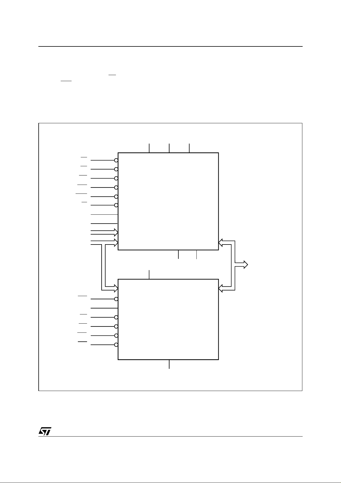
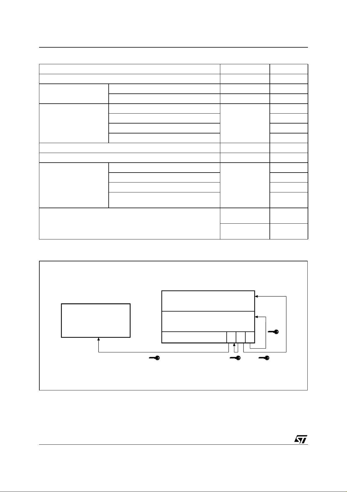
Table 1. Signal Names
A0-A18 Address Inputs
A19-A21 Address Inputs for Flash Chip only
DQ0-DQ15 Data Input/Output
V
V
DDF
DDQF
Flash Power Supply
Flash Power Supply for I/O Buffers
Figure 2. Logic Diagram
V
DDQF
V
DDF
22
A0-A21
EF
GF
WF
RPF
WPF
LF
KF
E1S
E2S
GS
WS
UBS
LBS
M36WT864TF
M36WT864BF
V
PPF
V
DDS
16
DQ0-DQ15
WAITF
V
PPF
V
SSF
V
SSQF
V
DDS
V
SSS
NC Not Connected Internally
DU Do Not Use as Internally Connected
Flash control functions
LF
EF
GF
WF
RPF
WPF
KF Flash Burst Clock
WAITF Wait Data in Burst Mode
SRAM control function s
Flash Optional Supply Voltage for Fast
Program & Erase
Flash Ground
Flash Ground for I/O Buffers
SRAM Power Supply
SRAM Ground
Latch Enable input
Chip Enable input
Output Enable input
Write Enable input
Reset input
Write Protect input
V
SSF
V
SSQF
V
SSS
AI06270
, E2S Chip Enable inputs
E1S
GS
WS
UBS
LBS
Output Enable input
Write Enable input
Upper Byte Enable input
Lower Byte Enable input
7/92
M36WT864TF, M36WT864BF
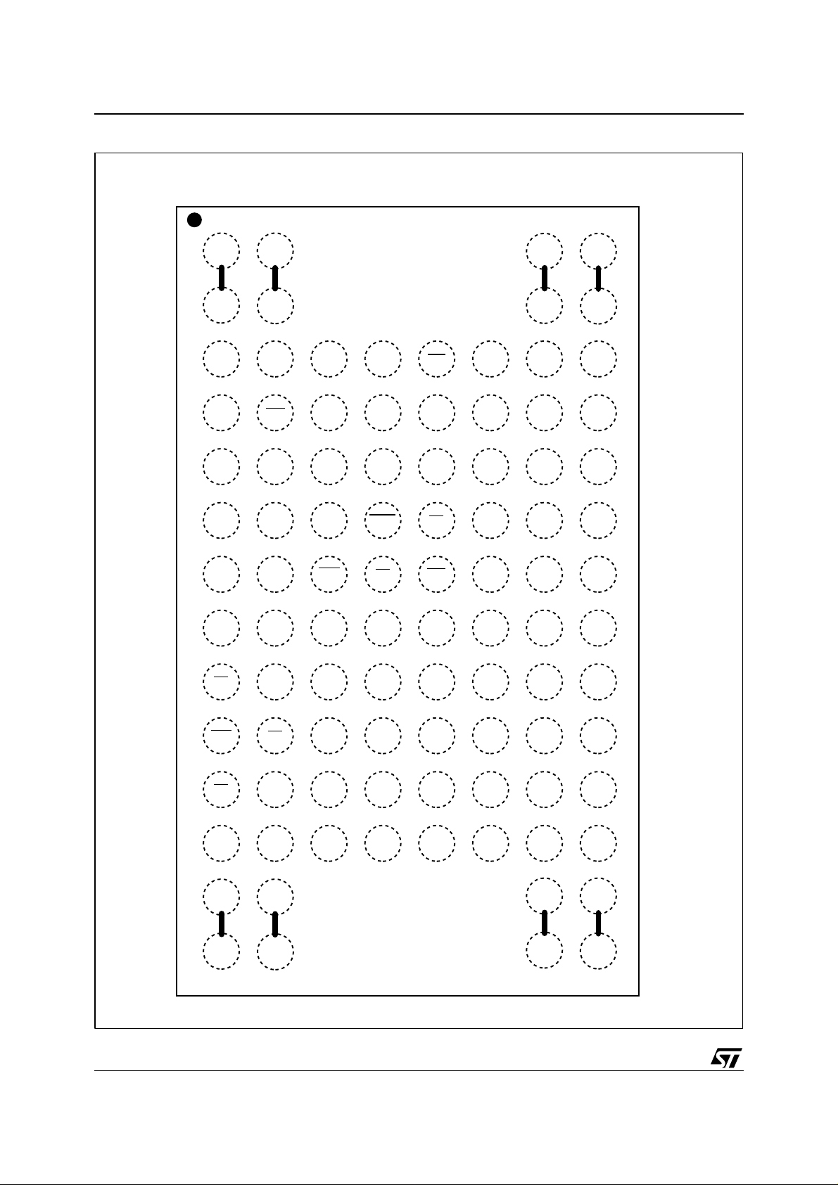
Figure 3. LFBGA Connections (Top view through package)
87654321
#A
#B
NC
NC
A
B
C
D
E
F
A4
A5
A3
A2
A1
A0
NC
NC
NCNC
NC
A21KF
NCV
A9V
A10A20
A14A8
WAITF
V
WS
E2SV
DDF
LFWPFNCA7
WFRPUBSA6
DQ5DQ10DQ2DQ8
DDS
SSF
DQ13
A19A18
NCLBS
NCA17
V
V
SSS
SSS
PPF
NC
A11
A12
A13
A15
A16
DU
8/92
G
#C
#D
GS
V
E1S
EF
SSS
NC
NC
V
SSQF
NC
NC
H
J
K
DQ1DQ0
DUDU
V
DDQF
DQ3
V
DDS
V
DDF
DQ12
DQ4DQ11DQ9GF
V
DDS
V
SSS
DU
V
SSQF
DQ7DQ14
DQ15DQ6
V
DDQF
V
SSF
NC
NC
V
V
DU
DU
SSS
SSS
NC
NC
AI06271

SIGNAL DESCRIPTIONS
See Figure 2 Logic Diagram and T able 1,Signal
Names, for a brief overview of the signals connected to this de vice.
Address Inputs (A0-A18). Addresses A0-A18
are common inputs for the Flash an d the SRAM
components. The Address Inputs select the cells
in the memory array to access during Bu s Read
operations. During Bus Write operations they control the commands sent to the Command Interface
of the internal state machine. The Flash memory is
accessed through the Chip Enable (
Enable (WF
) signals, while the SRAM is accessed
through two Chip Enable signals (E1S
and the Write Enable signal (WS
EF) and Write
and E2S)
).
Address Inputs (A19-A21). Addresses A19-A21
are inputs for the Flash component only. The
Flash memory is acc essed through the Chip E nable (EF
) and Write Enable (WF) signals.
Data Input/Output (DQ0-DQ15). The Data I/O
outputs the data stored at the selected address
during a Bus Read operation or inputs a command
or the data to be programmed durin g a Write Bus
operation.
Flash Chip Enable (EF
). The Chip Enable input
activates the memory control logic, input buffers,
decoders and sense amplifiers. When Chip Enable is at V
tive mode. When Chip Enable is at V
andReset is at VIH the device is in ac-
IL
IH
the
memory is deselected, the outputs are high impedance and the power consumption is reduced to the
stand-b y l e v el.
Flash Output Enable (GF
). The Output Enable
controls data outputs during the Bus Read operati on of the memo ry.
Flash Write Enable (
WF). The Write Enable
controls the Bus Write operation of the memory’s
Command Interface. The data and address inputs
are latched on the rising ed ge of Chip Enable or
Write Enable whichever occurs first.
Flash Write Protect (WPF
). Write Protect is an
input that gives an additional hardware protection
for each block. When Write Protect is at V
IL
, the
Lock-Down is enabled and the protection status of
the Locked-Down blocks cannot be changed.
When Write Protect is at V
, the Lock-Down is
IH
disabled and the Locked-Down blocks can be
locked or unlocked. (refer to Table 13, Lock Status).
Flash Reset (RPF
). The Reset input provides a
hardware reset of the memory. When Re set is at
V
, the memory is in reset mode: the outputs are
IL
high impedance and the current consumption is
reduced to the Reset Supply Current I
. Refer to
DD2
Table 2, DC Characteristics - Currents for the value of I
After Reset all blocks are in the Locked
DD2.
state and the Configuration Register is reset.
M36WT864TF, M36WT864BF
When Reset is at V
eration. Exiting reset mode the device enters
asynchronous read mod e, but a negative transition of Chip Enable or Lat ch E nable is required to
ensure valid data outputs.
The Reset pin can be interfaced with 3V logic without any additional circuitry . It can be t ied to V
(refer to Table 19, DC Characteristics).
Flash Latc h En abl e (LF
the address bits on its rising edge. The address
latch is transparent when Latch Enable is at V
and it is inhibited when Latch Enable is at VIH.
Latch Enable can be kept Low (also at board level)
when the Latch Enable function is not required or
supported.
Flash Clock (KF). The clock input synchronizes
the Flash memory to the microcontroller during
synchronous read operations; the address is
latched on a Clock edge (rising or falling, acc ording to the configuration settings) when L atch Enable is at VIL. Clock is don't care during
asynchronous read and in write operations.
Flash Wait ( WAITF). Wait is a Flash output signal
used during synchronous read to indicate whether
the data on the output bus are valid. This output is
high impedance when Flash Chip Enable is at V
or Flash Reset is at VIL. It can be configured to be
active during the wait cycle or one clock cycle in
advance. The WAITF signal is not gated by Output
Enable.
SRAM Chip Enable (E1S
able inputs activate the SRAM memory control
logic, input buffers and decoders. E1S
E2S at V
deselects the memory and reduces the
IL
power consumption to the standby level. E1S
E2S can also be used to control writing to the
SRAM memory array, while WS
is not allowed to set EF
at the same time.
at V
IH
SRAM Write Enable (WS
put controls writing to the SRA M memory array.
WS
is active low.
SRAM Output Enable (GS)
gates the outputs through the data buffers during
a read operation of t he S RAM mem ory. GS
tive low.
SRAM Upper Byte Enable (UBS)
Byte Enable input enables the upper byte for
SRAM (D Q8-D Q15). U BS
SRAM Lower Byte Enable (LBS
Byte Enable input enables the lower byte for
SRAM (DQ0- D Q 7). L BS
Supply Voltage. V
V
DDF
supply to the internal core of the Flash memory de-
, the device is in normal op-
IH
). Latch Enable latches
, E2S). The Chip En-
at VIH or
remains at V
at V
E1S at VIL and E2S
IL,
). The Write Enable in-
. The Output Ena ble
is ac-
. The Upper
is active low .
). The Lower
is active low.
provides the power
DDF
RPH
and
It
IL.
IL
IH
9/92

M36WT864TF, M36WT864BF
vice. It is the main power supply for all Flash operations (Read, Program and Erase).
V
DDQF
and V
Supply Voltage. V
DDS
DDQF
provides the power supply for the Flash mem ory I/O
pins and V
provides the power supply for the
DDS
SRAM control and I/O pins. This allows all Outputs
to be powered independently from t he Flash core
power supply, V
DDF
. V
can be tied to V
DDQF
DDS
or
it can use a separate supply.
V
Program Supp ly Vol tage. V
PPF
is both a
PPF
Flash control input and a Flash power supply pin.
The two functions are selected by the voltage
range applied to the pin.
is kept in a low voltage range (0V to V
If V
PPF
V
is seen as a control input. In this case a volt-
PPF
age lower than V
gives an absolute protec-
PPLKF
tion against program or erase, while V
PPF
> V
DDQF
PP1F
enables these functions (s ee Tables 18 and 19,
DC Characteristics for the relevant values). V
PPF
is only sampled at the b eginning of a program or
erase; a change in its value after the operation has
started does not have any effect and program or
erase operations continue.
If V
is in the range of V
PPF
supply pin. In this condition V
it acts as a power
PPHF
must be stable
PPF
until the Program/Erase algorithm is completed.
V
SSF ,VSSQF
and V
SSS
and V
are the ground references for all voltage
Grounds. V
SSS
SSF
measurements in the Flash (core and I/O Buffers)
and SRAM chips, respectively.
Note: Each device in a system should have
and V
V
DDF
capacitor close to the pin (high frequency, in-
)
decoupled with a 0.1µF ceramic
PPF
herently low inductance ca pacitors should b e
as close as possible to the package). See Figure 10, AC Measurement Load Circuit. The
PCB trace widths shou ld be sufficien t to ca rry
the required V
program and erase currents.
PPF
, V
SSQF
10/92
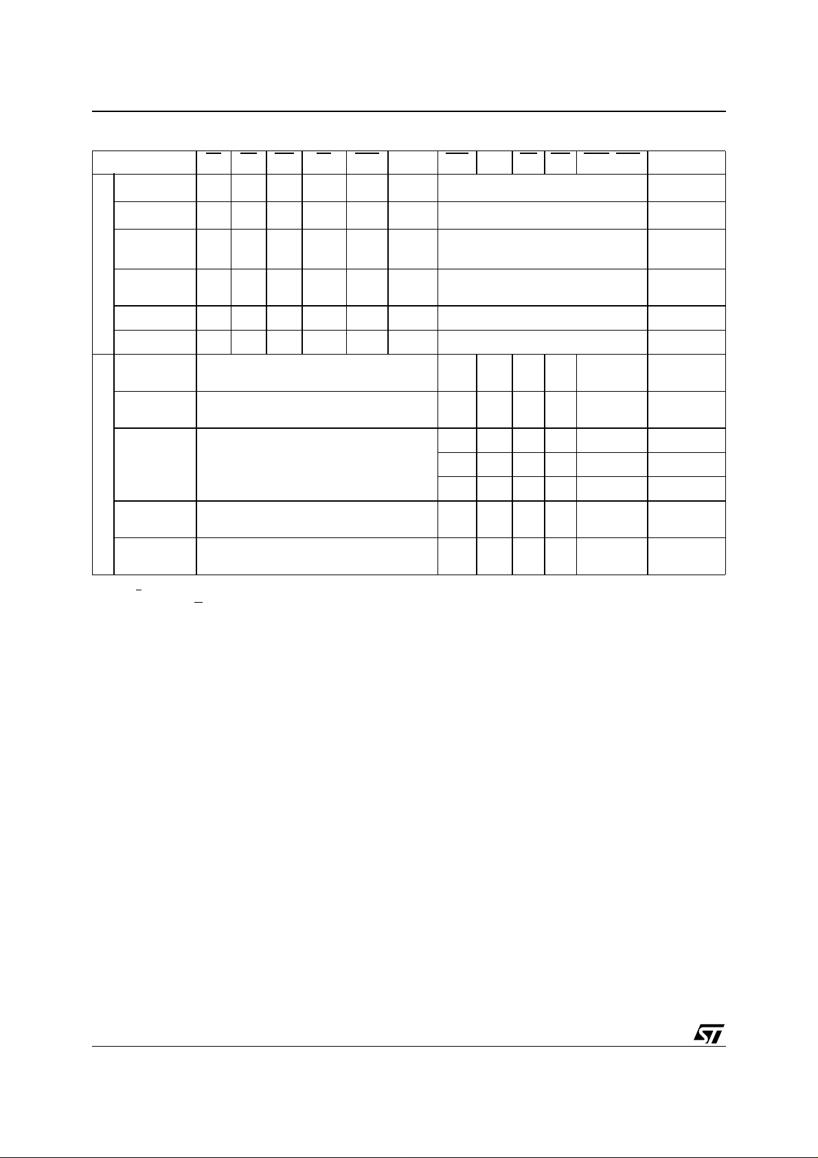
FUNCTIONAL DESCRIPTION
The Flash and SRAM components have separate
power supplies and grounds and are distinguished
by three chip enable inputs: EF
ory and, E1S
and E2S for the SRAM.
for the Flash mem-
Recommended operating conditions do not allow
both the Flash and the SRAM to be in active mode
at the same time. The most common example is
Figure 4. Func ti onal Block Di a gram
M36WT864TF, M36WT864BF
simultaneous read operations on the Flash and
the SRAM which would resul t in a data bus contention. Therefore it is recommended to put the
SRAM in the h igh impedance state whe n reading
the Flash and vice versa (see Table 2 Main Operation Modes for details).
EF
GF
WF
RPF
WPF
LF
WAITF
KF
A19-A21
A0-A18
E1S
E2S
GS
WS
UBS
LBS
V
DDF
Flash Memory
64 Mbit (x16)
V
DDS
8 Mbit (x 16)
V
DDQF
V
SRAM
SSQF
V
PPF
V
SSF
DQ0-DQ15
V
SSS
AI06272
11/92
M36WT864TF, M36WT864BF
Table 2. Main Operation Modes
Operation Mode EF GF WF LF RPF WAITF E1S E2S GS WS UBS, LBS DQ15-DQ0
Bus Read
Bus Write
Address
Latch
V
ILVILVIH
V
ILVIHVIL V
V
IL
V
X
IH
(2)
V
V
V
(2)
IH
V
IH
V
IH
IL
IL
IL
SRAM must be disabled Data Output
SRAM must be disabled Data Input
SRAM must be disabled
Data Output
or Hi-Z
(3)
Output
Disable
Flash Memory
Standby
V
ILVIHVIH
V
XX X
IH
Reset X X X X
V
X
IH
V
IH
V
IL
Hi-Z Any SRAM mode is allowed Hi-Z
Hi-Z Any SRAM mode is allowed Hi-Z
Read Flash must be disabled
Write Flash must be disabled
Standby/
Power Down
SRAM
Data
Any Flash mode is allowable
Any Flash mode is allowable
Retention
Output
Disable
Note: 1. X = Don' t care.
can be tied to VIH if the valid address has been previously latched.
2. L
3. Depends on G
4. WAIT signal pol arity is conf i gured using t he Set Confi guration Register command.
Any Flash mode is allowable
.
SRAM must be disabled Hi-Z
V
VIHVILV
IL
V
V
IL
IH
V
X X X X Hi-Z
IH
V
X
IL
IH
V
X
IL
X X X Hi-Z
XXXX
V
V
IH
V
IL
X X X Hi-Z
IL
VIHVIHV
IH
V
IL
V
IL
V
IH
X Hi-Z
Data out
Word Read
Data in
Word Write
Hi-Z
12/92

M36WT864TF, M36WT864BF
Flash Memory Component
The Flash memory is a 64 Mbit (4Mbit x16) nonvolatile Flash memory that may be erased electrically at block level and programmed in-system on
a Word-by-Word basis using a 1.65V to 2.2V V
supply for the circuitry and a 1.65V to 3.3V V
DD
DDQ
supply for the Input/Output pins. An optional 12V
V
power supply is provided to s peed up cus-
PPF
tomer programming.
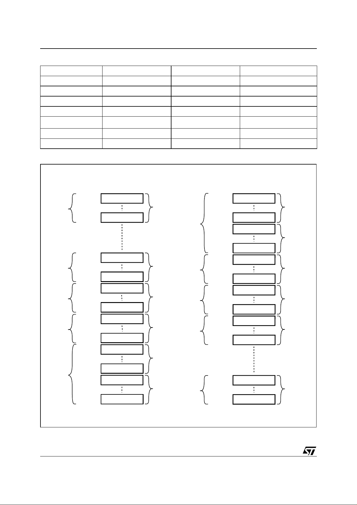
The device features an asymmetr ical block archi-
tecture with an array of 135 blo cks divided into 4
Mbit banks. There are 15 banks each containing 8
main blocks of 32 KWords, and one parameter
bank containing 8 parameter blocks of 4 KWords
and 7 main blocks of 32 KWords. The Multiple
Bank Architecture allows Dual Operations, while
programming or erasing in one bank, Read operations are possible in other banks. Only one bank at
a time is allowed to be in Program or Erase mode.
It is possible to perform burst reads that cross
bank boundaries. The bank architecture is summarized in Table 3, and the memory maps are
shown in Figure 5. The Parameter Blocks are located at the top of t he m em ory ad dres s s pace f or
the M36WT864TF, and at the bottom for the
M36WT864BF.
Each block can be erased separately. Erase can
be suspended, in order to perform program in any
other block, and then resum ed. Program can be
suspended to read data in any other block and
then resumed. Each block can be programmed
and erased over 100,000 cycles using the supply
voltage V
. There are two Enhanced Factory
DD
programming commands available to speed up
programming.
Program and Erase command s are written to the
Command Interface of the memory. An internal
Program/Erase Controller takes care of the timings necessary for program and erase operations.
The end of a program or erase operation can be
detected and any error conditions identified in the
Status Register. The command set required to
control the memory is consistent with JEDEC standards.
The device supports synchronous burst read and
asynchronous read from all blocks of the me mory
array; at power-up the device is configured for
asynchronous read. In synchronous burst mode,
data is output on each clock cycle at frequencies
of up to 54MHz.
The device features an Aut oma tic Standby m ode.
During asynchronous read operations, after a bus
inactivity of 150ns, the device automatically
switches to the Automatic Standby m ode. In this
condition the power consumption is reduced to the
standby value I
and the outputs are still driven.
DD4
The Flash memory features an instant, individual
block locking scheme that allows any block to be
locked or unlocked with no latency, enabling instant code and data protection. All blocks have
three levels of protection. They can be locked and
locked-down individually preventing any accidental programming or erasure. There is an additional
hardware protection against program and erase.
When V
PPF
≤ V
all blocks are protected
PPLK
against program or erase. All blocks are locked at
Power- Up.
The device includes a Protection Re gister and a
Security Block to increase the protectio n of a s ystem’s design. The Protection Register is divided
into two segments: a 64 bit segment c ontaining a
unique device number written by ST, and a 128 bit
segment One-Time-Programmable (OTP) by the
user. The user programmable segment can be
permanently protected. The Security Block, parameter block 0, can be permanently protected by
the user. Figure 6, shows the Security Block and
Protection Register Memory Map.
SRAM Comp onent
The SRAM is an 8 Mbit (512Kb x16) asynchronous
random access memory which features a super
low voltage operation and low current consumption with an access time of 70ns. The memory operations can be performed using a single low
voltage supply, 2.7V to 3.3V.
13/92
M36WT864TF, M36WT864BF
Table 3. Flash Bank Architecture
Number Bank Size Parameter Blocks Main Blocks
Parameter Bank 4 Mbits 8 blocks of 4 KWords 7 blocks of 32 KWords
Bank 0 4 Mbits - 8 blocks of 32 KWords
Bank 1 4 Mbits - 8 blocks of 32 KWords
Bank 2 4 Mbits - 8 blocks of 32 KWords
----
Bank 13 4 Mbits - 8 blocks of 32 KWords
Bank 14 4 Mbits - 8 blocks of 32 KWords
Figure 5. Flash Block Addresses
Top Boot Block
Address lines A21-A0
Bank 14
Bank 2
Bank 1
Bank 0
Parameter
Bank
000000h
007FFFh
038000h
03FFFFh
300000h
307FFFh
338000h
33FFFFh
340000h
377FFFh
378000h
37FFFFh
380000h
387FFFh
3D8000h
3BFFFFh
3C0000h
3C7FFFh
3F0000h
3F7FFFh
3F8000h
3F8FFFh
3FF000h
3FFFFFh
32 KWord
32 KWord
32 KWord
32 KWord
32 KWord
32 KWord
32 KWord
32 KWord
32 KWord
32 KWord
4 KWord
4 KWord
----
8 Main
Blocks
8 Main
Blocks
8 Main
Blocks
8 Main
Blocks
7 Main
Blocks
8 Parameter
Blocks
Parameter
Bank
Bank 0
Bank 1
Bank 2
Bank 14
----
000000h
000FFFh
007000h
007FFFh
008000h
00FFFFh
038000h
03FFFFh
040000h
047FFFh
078000h
07FFFFh
080000h
087FFFh
0B8000h
0BFFFFh
0C0000h
0C7FFFh
0F8000h
0FFFFFh
3C0000h
3C7FFFh
3F8000h
3FFFFFh
Bottom Boot Block
Address lines A21-A0
4 KWord
4KWord
32 KWord
32 KWord
32 KWord
32 KWord
32 KWord
32 KWord
32 KWord
32 KWord
32 KWord
32 KWord
----
8 Parameter
Blocks
7 Main
Blocks
8 Main
Blocks
8 Main
Blocks
8 Main
Blocks
8 Main
Blocks
14/92
AI06273

FLASH BUS OPERATIONS
There are six standard bus operations that control
the Flash device. These are Bus Read, Bus Write,
Address Latch, Ou tput Disable, Standby and Reset. See Table 2, Main Operating Modes, for a
summary.
Typically glitches of less than 5ns on Chip Enable
or Write Enable are ignored by the memory and do
not affect Bus Write operations.
Bus Read. Bus Read operations are used to output the contents of the Memory Array, the Electronic Signature, the Status Register and the
Common Flash Interface. Both Chip Enable and
Output Enable must be at V
in order to perform a
IL
read operation. The Chip Enable input should be
used to enable the device. Out put Enable should
be used to gate data onto the output. The data
read depends on the previous command written to
the memory (see Command Interface section).
See Figures 11, 12, 13 and 14 Read AC Waveforms, and Tables 21 and 22 Read AC Characteristics, for details of when the output becomes
valid.
Bus Write. Bus Write operations write Commands to the memory or latch Input Data to be
programmed. A bus write operation is initiated
when Chip Enable and Write Enable are at V
Output Enable at V
. Commands, Input Data and
IH
IL
with
Addresses are latched on the rising edge of Write
Enable or Chip Enable, whichever occurs first. The
addresses can also be latched prior to the write
operation by toggling Latch E nable. In this case
M36WT864TF, M36WT864BF
the Latch Enable shoul d be t ied to V
bus write operation.
See Figures 16 and 17, Write AC Waveforms, and
Tables 23 and 24, Write AC Characteristics, for
details of the timing requirements.
Address Latch. Address latch operations input
valid addresses. Both Chip enable and Latch Enable must be at V
during address latch opera-
IL
tions. The addresses are latched on the rising
edge of Latch Enable.
Output Disa bl e . The outputs are high impedance when the Output Enable is at V
Standby. Standby di sables most of the internal
circuitry allowing a substantial reduction of the current consumption. The memory is in stand-by
when Chip Enable and Reset are at V
er consumption is reduced to the stand-by level
and the outputs are s et to high impedan ce, independently from the Output Enable or Write Enable
inputs. If Chip Enable switches to V
gram or erase operation, the device enters Standby mode when finished.
Reset. During Reset mode the memory is deselected and the outputs are high impedance. The
memory is in Reset mode when Reset is at V
The power consumption is reduced to the Standby
level, independently from the Chip Enable, Output
Enable or Write Enable inputs. If Reset is pulled to
V
during a Program or Erase, this operation is
SS
aborted and the memory content is no longer valid.
during the
IH
.
IH
. The pow-
IH
during a pro-
IH
IL
.
15/92

M36WT864TF, M36WT864BF
FLASH COMMAND INTERFACE
All Bus Write operations t o the me mory are in terpreted by the Command Interface. Commands
consist of one or more sequential Bus Write operations. An internal Program/Erase Controller handles all timings and verifies the correct execution
of the Program and Erase commands. The Program/Erase Controller provides a Status Regi ster
whose output may be read at any ti me to monitor
the progress or the result of the operation.
The Command Interface is reset to read mode
when power is first applied, when exiting from Reset or whenever V
mand sequences must be followed exactly. Any
invalid combination of commands will reset the device to read mode.
Refer to Table 4, Command C odes and Appendix
D, Tables 44, 45, 46 and 47, Command I nterface
States - Modify and Lock Tables, for a summary of
the Command Interface.
The Command Interface is split into two type s of
commands: Standard commands and Factory
Program commands. The following sections explain in detail how to perform each command.
is lower than V
DD
LKO
. Com-
Table 4. Command Codes
Hex Code Command
01h Block Lock Confirm
03h Set Configuration Register Confirm
10h Alternative Program Setup
20h Block Erase Setup
2Fh Block Lock-Down Confirm
30h Enhanced Factory Program Setup
35h Double Word Program Setup
40h Program Setup
50h Clear Status Register
56h Quadruple Word Program Setup
Block Lock Setup, Block Unlock Setup,
60h
70h Read Status Register
75h
80h Bank Erase Setup
90h Read Electronic Signature
Block Lock Down Setup and Set
Configuration Register Setup
Quadruple Enhanced Factory Program
Setup
98h Read CFI Query
B0h Program/Erase Suspend
C0h Protection Register Program
Program/Erase Resume, Block Erase
D0h
FFh Read Array
Confirm, Bank Erase Confirm, Block
Unlock Confirm or Enhanced Factory
Program Confirm
16/92

COMMAND INTERFACE - STANDARD COMMANDS
The following commands are the basic commands
used to read, write to and configure the device.
Refer to Table 5, Standard Commands, in conjunction with the following text descriptions.
Read Array Command
The Read Array command re turns the addressed
bank to Read Array mode. One Bus Write cycle is
required to issue the Read Array command and return the addressed bank to Read Array mode.
Subsequent read operations will read the addressed location and output t he data. A Read Array command can be issued in one bank while
programming or erasing in another bank. However
if a Read Array command is issued to a bank currently executing a Program or Erase operation the
command will be e xecuted but the output da ta is
not guaranteed.
Read Status Register Command
The Status Register indi cates when a Program or
Erase operation is complete and the success or
failure of operation itself. Issue a Read Status
Register command to read the Status Register
content. The Read Status Register com man d c an
be issued at any time, even during Program or
Erase operations.
The following read operations output the content
of the Status Register of the addressed bank. The
Status Register is latched on the falling edge of E
or G signals, and c an b e read until E or G returns
to V
. Either E or G must be toggled to update the
IH
latched data. See Table 8 for the description of the
Status Register Bits. This mode supports asynchronous or single synchronous reads only.
Read Electronic Signature Command
The Read Electronic Signature command reads
the Manufacturer and Device Codes, the Block
Locking Status, the Protection Register, and the
Configuration Register.
The Read Electronic Signature command consists
of one write cycle to an address within one o f the
banks. A subsequent Read ope ra tion in the sam e
bank will output the Manufacturer Code, the Device Code, the protection Status of the blocks in
the targeted bank, the Protection Register, or the
Configuration Register (see Table 6).
If a Read Electronic Signature command is issued
in a bank that is executing a Program or Erase operation the bank will go into Read Electronic Signature mode, subsequent Bus Read cycles will
output the Electronic Sign ature data an d the Program/Erase controller will continue t o program or
erase in the background. This mode supports
asynchronous or single synchronous reads only, it
does not support page mode or synchronous burst
reads.
M36WT864TF, M36WT864BF
Read CFI Query Command
The Read CFI Query command is used to read
data from the Common Flash Interface (CFI). The
Read CFI Query Command consists of one Bus
Write cycle, to an address within one of the banks.
Once the command is issued subsequent Bus
Read operations in the sam e bank read from the
Common Flash Interface.
If a Read CFI Query command is issued in a bank
that is executing a Program or Erase operation the
bank will go into Read CFI Query mo de, subsequent Bus Read cycles will output the CFI data
and the Program/Erase con troller will continue to
Program or Erase in the background. This m ode
supports asynchronous or single synchronous
reads only, it does not support page mode or synchronous burst reads.
The status of the other banks is not affected by the
command (see Table 11). After issuing a Read
CFI Query command, a Read Array command
should be issued to t he address ed bank to return
the bank to Read Array mode.
See Appendix C, Common Flash Interface, Tables
34, 35, 36, 37, 38, 40, 41, 42 and 43 for details on
the information contained in the Common Flash Interface memory area.
Clear Status Register Command
The Clear Status Register comm and can be used
to reset (set to ‘0’) error bits 1, 3, 4 and 5 in the Status Register. One bus write cycle is required to issue the Clear Status Register command. After the
Clear Status Register command the bank returns
to read mode.
The error bits in the Status Regi ster do not automatically return to ‘0’ when a new command is issued. The error bits in the Status Register should
be cleared before attempting a new Program or
Erase command.
Block Erase Command
The Block Erase com mand can be used to erase
a block. It sets all the bits within the selected block
to ’1’. All previous data in the b lock is lost. If the
block is protected then the Erase operation will
abort, the data in the block will not be changed and
the Status Register will output the error. The Block
Erase command can be issued at any moment, regardless of whether the block has been programmed or not.
Two Bus Write cycles are required to issue the
command.
■ The first bus cycle sets up the Erase command.
■ The second latches the block address in the
internal state machine and starts the Program/
Erase Controller.
17/92

M36WT864TF, M36WT864BF
If the second bus cycle is not Write Erase Confirm
(D0h), Status Register bits 4 and 5 are set and the
command aborts. Erase aborts if Reset turns to
. As data integrity cannot be guaranteed when
V
IL
the Erase operation is aborted, the block m ust be
erased again.
Once the command is issued the device outputs
the Status Register data when any address within
the bank is read. At the end o f the operation the
bank will remain in Read Status Register mode until a Read Array, Read CFI Query or Read Electronic Signature command is issued.
During Erase operations the bank containing the
block being erased will only accept the Read Array, Read Status Register, Read Electronic Signature, Read CFI Query and the Program/Erase
Suspend command, all other commands will be ignored. Refer to Dual Operations section for detailed information about simultaneous operations
allowed in banks not being e rased. Typical Erase
times are given in Table 14, Program, Erase
Times and Program/Erase Endurance Cycles.
See Appendix C, Figure 32, Block Erase Flowchart and Pseudo Code, for a suggested flowchart
for using the Block Erase command.
Bank Erase Command
The Bank Erase command can be used to erase a
bank. It sets all the bits within the selected bank to
’1’. All previous data in the bank is lost. The B ank
Erase command will igno re any protected blocks
within the bank. If all blocks in the bank are protected then the Bank Erase operation will abort
and the data in the bank wi ll not b e changed. The
Status Register will not output any error.
Two Bus Write cycles are required to issue the
command.
■ The first bus cycle sets up the Bank Erase
command.
■ The second latches the bank address in the
internal state machine and starts the Program/
Erase Controller.
If the second bus cycle is not Write Bank Erase
Confirm (D0h), Status Register bits SR4 and S R5
are set and the command aborts. Erase aborts if
Reset turns to V
. As data integrity cannot be
IL
guaranteed when the Erase operation is aborted,
the bank must be erased again.
Once the command is issued the device outputs
the Status Register data when any address within
the bank is read. At the end o f the operation the
bank will remain in Read Status Register mode until a Read A rray, Read CFI Query o r Read Electronic Signature command is issued.
During Bank Erase operations the bank being
erased will only accept the Read Array, Read Status Register, Read Electronic Signature and Read
CFI Query command, all other commands will be
ignored. A Bank Erase operation ca nnot be suspended.
Refer to Dual Operations section for detailed information about simultaneous operations allowed in
banks not being erased. Typical Erase times are
given in Table 14, Program, Erase Times and Program/Erase Endurance Cycles.
Program Command
The memory array can be programmed word-byword. Only one Word in one bank can be programmed at any one time. Two bus write cycles
are required to issue the Program Command.
■ The first bus cycle sets up the Program
command.
■ The second latches the Address and the Data to
be written and starts the Program/Erase
Controller.
After programming has started, read operations in
the bank being programmed output the Status
Register content.
During Program operations the bank being programmed will only accept the Read Array, Read
Status Register, Read Electronic Signature, Read
CFI Query and the Program/Erase Suspen d command. Refer to Dual Operations section for detailed information about simultaneous operations
allowed in banks not bei ng programmed. Typical
Program times are given in Table 14, Program,
Erase Times and Program/Erase Endurance Cycles .
Programming aborts if Reset goes to V
. As data
IL
integrity cannot be guaranteed when the program
operation is aborted, the memory location must be
reprogrammed.
See Appendix C, Figure 28, Program Flowchart
and Pseudo Code, for the f lowchart for using the
Program command.
Program/Erase Suspend Command
The Program/Erase Suspend command is used to
pause a Program or Block Erase operation. A
Bank Erase operation cannot be suspended.
One bus write cycle is required to issue the P rogram/Erase command. O nce the Program/Erase
Controller has paused bits SR7, SR6 and/ or SR2
of the Statu s Regist er will be s et to ‘1’. Th e command can be addressed to any bank.
During Program/Erase Suspend the Command Interface will accept the Program/Erase Resume,
Read Array (cannot read the suspended block),
Read Status Register, Read Electronic S ignature
and Read CFI Q uery commands. Additionally, if
the suspend operation was Erase then the Clear
status Register, Program, Block Lock, Block LockDown or Block Unlock commands will also be accepted. The block being erased may be protected
18/92

M36WT864TF, M36WT864BF
by issuing the Block Lock, Block Lock-Down or
Protection Register Program commands. Only the
blocks not being erased may be read or programmed correctly. When the Program/Erase Resume command is issued the operation will
complete. Refer to the Dual Operations section for
detailed information about simultaneous operations allowed during Program/Erase Suspend.
During a Program/Erase Suspend, the device can
be placed in standby mode by taking Chip Enable
. Program/Erase is aborted if Reset turns to
to V
IH
V
.
IL
See Appendix C, Figure 31 , Program Suspend &
Resume Flowchart and Pseudo Code, and Figure
33, Erase Suspend & Resume Flowchart and
Pseudo Code for flowcharts for using the Program/
Erase Suspend command.
Program/Erase Resume Command
The Program/Erase Resume command can be
used to restart the Program/Erase Controller after
a Program/Erase Suspen d command has paused
it. One Bus Write cycle is required to issue the
command. The command can be written to any
address.
The Program/Erase R esume command d oes not
change the read m ode of the banks. If the s uspended bank was in Read Status Register, Read
Electronic signature or Read CFI Query mode the
bank remains in that m ode and outputs the corresponding data. If the bank was in Read Array
mode subsequent read operations will output invalid data.
If a Program command is issued during a Block
Erase Suspend, then the erase cannot be resumed until the programming operation has completed. It is possible to accumulate suspend
operations. For example: suspend an eras e operation, start a programming operation, suspend the
programming operation then read the array. See
Appendix C, Figure 31, Program Susp end & Resume Flowchart and Pseudo Code, and Figure 33,
Erase Suspend & Resume Flowchart and Pseudo
Code for flowcharts for using the Program/Erase
Resume command.
Prot e ction R e gister P rogram C om m and
The Protection Register Program command is
used to Program the 128 bit user O ne-Time-Programmable (OTP) segment of the Protection Register and the Protection Register Lock. The
segment is programmed 16 bits at a time. When
shipped all bits in the segment are set to ‘1’. The
user can only program the bits to ‘0’.
Two write cycles are required to issue the Protection Register Program command.
■ The first bus cycle sets up the Protection
Register Program command.
■ The second latches the Address and the Data to
be written to the Protection Register and starts
the Program/Erase Controller.
Read operations output the Status Register content after the programming has started.
The segment can be protected by programming bit
1 of the Protection Lock Register. Bit 1 of the Protection Lock Register also protects bit 2 of the Protection Lock Register. Programming bit 2 of the
Protection Lock Register will result in a permanent
protection of Parameter B lock #0 (see Figure 6,
Security Block and Protection Register Memory
Map). Attempting to program a previously protected Protection Register will result in a Status Register error. The protection of the Protection
Register and/or the Security Block is not reversible.
The Protection Register Program cannot be suspended. See Appendix C, Figure 35, Protection
Register Program Flowchart and Pseudo Code,
for a flowchart for using the Protection Register
Program command.
Set Configuration Regi s te r C om m and.
The Set Configuration Register command is used
to write a new value to the Burst Configuration
Control Register which defines the burst length,
type, X latency, Synchronous/Asynchronous Read
mode and the valid Clock edge configuration.
Two Bus Writ e cycle s are required to issue th e Se t
Configuration Register command.
■ The first cycle writes the setup command and
the address corresponding to the Configuration
Register content.
■ The second cycle writes the Configuration
Register data and the confirm command.
Once the command is issued the memory returns
to Read mode.
The value for the Configuration Register is always
presented on A0-A15. CR0 is on A0, C R1 on A1,
etc.; the other address bits are ignored.
Block Lock Command
The Block Lock command is used to lock a block
and prevent Program or Erase operations from
changing the data in it. All blocks are locked at
power-up or reset.
Two Bus Write cycles are required to issue the
Block Lock command.
■ The first bus cycle sets up the Block Lock
command.
■ The second Bus Write cycle latc hes the blo ck
address.
The lock status can be monitored for each block
using the Read Electronic Signature command.
Table. 13 shows the Lock Status after issuing a
Block Lock command.
19/92

M36WT864TF, M36WT864BF
The Block Lock bits are volatile, once set they remain set until a hardware reset or power-down/
power-up. They are cleared by a Block Unlock
command. Refer to the section, Block Locking, for
a detailed explanation. See Appendix C, Figure
34, Locking Operations Flowchart and Pseudo
Code, for a flowchart for using the Lock command.
Block Unlock Command
The Block Unlock command is used to unlock a
block, allowing the block to be programmed or
erased. Two Bus Write cycles are requ ired to issue the Block Unlock command.
■ The first bus cycle sets up the Block Unlock
command.
■ The second Bus Write cycle latc hes the blo ck
address.
The lock status can be monitored for each block
using the Read Electronic Signature command.
Table 13 shows the protection status after issuing
a Block Unlock command. Refer to the section,
Block Locking, for a detailed expla nation and A ppendix C, Figure 34, Locking Operations Flowchart and Pseudo Code, f or a flowchart for using
the Unlock command.
Block Lock-Down Command
A locked or unlocked block can be locked-down by
issuing the Block Lock-Down command. A lockeddown block cannot be programm ed or erased, or
have its protection status changed when WP
low, V
. When WP is high, V
IL
the Lock-Down
IH,
is
function is disabled and the lock ed blocks can be
individually unlocked by the Block Unlock command.
Two Bus Write cycles are required to issue the
Block Lock-Down command.
■ The first bus cycle sets up the Block Lock
command.
■ The second Bus Write cycle latc hes the blo ck
address.
The lock status can be monitored for each block
using the Read Electronic Signature command.
Locked-Down blocks revert to the locked (and not
locked-down) state when the device is reset on
power-down. Table. 13 shows the Lo ck Statu s after issuing a Block Lock-Down command. Refer to
the section, Block Locking, for a detailed explanation and Appendix C, Fi gure 34, Locking Operations Flowchart and Pseudo Code, for a flowchart
for using the Lock-Down command.
20/92
Table 5. Flash Standard Commands
M36WT864TF, M36WT864BF
Bus Operations
Commands
Cycles
Read Array 1+ Write BKA FFh
Read St atus Register 1+ Write BKA 70h Read
Read Electro nic Signature 1+ Write BKA 90h Read
Read CFI Query 1+ Write BKA 98h Read
Clear Status Register 1 Write BKA 50h
Block Erase 2 Write BKA 20h Write BA D0h
Bank Erase 2 Write BKA 80h Write BKA D0h
Program 2 Write BKA 40h or 10h Write WA PD
Program/Erase Suspend 1 Write X B0h
Program/Erase Resume 1 Write X D0h
Protection Register Program 2 Write PRA C0h Write
Set Configuration Register 2 Write CRD 60h Write
Block Lock 2 Write BKA 60h Write
Block Unlock 2 Write BKA 60h Write
Block Lock-Down 2 Write BKA 60h Write
Note: 1. X = Don't Care, WA=Word Address in targeted bank, RD=Read Data, SRD=Status Register Data, ESD=Electronic Signature Data,
QD=Query Dat a, BA=Bl ock Address, BK A= Ban k Address , PD= Program Data, PR A=Prot ectio n Regist er Addre ss, PRD =Prote ction
Register Dat a, CRD=Configurat ion Regist er Data.
2. Must be same bank as in the first cycle. The signatur e addresses are listed in Table 6.
Op. Add Data Op. Add Data
1st Cycle 2nd Cycle
Read
WA RD
(2)
BKA
(2)
BKA
(2)
BKA
PRA
CRD 03h
BA 01h
BA
BA
SRD
ESD
QD
PRD
D0h
2Fh
21/92
M36WT864TF, M36WT864BF
Table 6. Electronic Signature Codes
Code Address (h) Data (h)
Manufacturer Code Bank Address + 00 0020
Device Code
Top Bank Address + 01 8810
Bottom Bank Address + 01 8811
Lock
0001
Unlocked 0000
Block Protection
Block Address + 02
Locked and Locked-Down 0003
Unlocked and Locked-Down 0002
Reserved Bank Address + 03 Reserved
Configuration Register Bank Address + 05 CR
ST Factory Default
0006
Security Block Permanently Locked 0002
Protection Register Lock
OTP Area Permanently Locked 0004
Security Block and OTP Area Permanently
Locked
Bank Address + 80
Bank Address + 81
Bank Address + 84
0000
Unique Device
Number
Protection Register
Bank Address + 85
Bank Address + 8C
Note: CR=Con figuration Register.
OTP Area
Figure 6. Flash Security Block and Protection Register Memo ry Ma p
22/92
SECURITY BLOCK
Parameter Block # 0
8Ch
85h
84h
81h
80h
PROTECTION REGISTER
User Programmable OTP
Unique device number
Protection Register Lock 2 1 0
AI06181

COMMAND INTERFACE - FACTORY PROGRAM COMMANDS
The Factory Program commands are used to
speed up programming. They require V
V
. Refer to Table 7, Factory Program Com-
PPH
PPF
to be at
mands, in conjunction with the following text descrip tion s.
Double Word Program Command
The Double Word Program command improves
the programming throughput by writing a page of
two adjacent words in parallel. The two words
must differ only for the address A0.
Programming should not be attempted when V
is not at V
V
is below V
PPF
. The command can be executed if
PPH
but the result is not guaran-
PPH
PPF
teed .
Three bus write cycles are necessary to issue the
Double Word Program command.
■ The first bus cycle sets up the Double Word
Program Command.
■ The second bus cycle latches the Address and
the Data of the first word to be written.
■ The third bus cycle latches the Address and the
Data of the second word to be written and starts
the Program/Erase Controller.
Read operations in the bank bei ng programmed
output the Status Register content after the programming has started.
During Double Word Program operations the bank
being programmed will only ac cept the Read Array, Read Status Register, Read Electronic Signature and Read CFI Query command, all other
commands will be ignored. Dual operations are
not supported during Double Word Program operations and it is not recommended to suspend a
Double Word Program operation. Typical Program
times are given in Table 14, Program, Erase
Times and Program/Erase Endurance Cycles.
Programming aborts if Reset goe s to V
. As data
IL
integrity cannot be guaranteed when the program
operation is aborted, the memory locations mu st
be reprogrammed.
See Appendix C, Figure 29, Double Word Program Flowchart and Pseudo Code, for the flowchart for using the Double Word Program
command.
Quadruple Word Program Command
The Quadruple Word Program command improves the programming throughput by writing a
page of four adjacent words in parallel. The four
words must differ only for the addresses A0 and
A1.
Programming should not be attempted when V
is not at V
V
is below V
PPF
. The command can be executed if
PPH
but the result is not guaran-
PPH
PPF
teed .
Five bus write cycles are necessary to issue the
Quadruple Word Program command.
■ The first bus cycle sets up the Double Word
Program Command.
■ The second bus cycle latches the Address and
the Data of the first word to be written.
■ The third bus cycle latches the Address and the
Data of the second word to be written.
■ The fourth bus cycle latches the Address and
the Data of the third word to be written.
■ The fifth bus cycle latches the Ad dr es s and th e
Data of the fourth word to be written and starts
the Program/Erase Controller.
Read operations to the bank being programmed
output the Status Register content after the programming has started.
Programming aborts if Reset goes to V
integrity cannot be guaranteed when the program
operation is aborted, the memory locations m ust
be reprogrammed.
During Quadruple Word Program operations the
bank being programmed will only accept the Read
Array, Read Status Register, Read Electronic Signature and Read CFI Query command, all other
commands will be ignored.
Dual operations are not supported during Quadruple Word Program operations and it is not recommended to suspend a Quadrupl e Word Program
operation. Typical Program times are given in Table 14, Program, Erase Times and Program/Erase
Endurance Cycles.
See Appendix C, Figure 30, Quadruple Word Program Flowchart and Pseudo Code, for the flowchart for using the Quadruple Word Program
command.
Enhanced Factory Program Command
The Enhanced Factory Program command can be
used to program large streams of dat a within any
one block. It greatly reduces the total programming time when a large number of Words are written to a block at any one time.
The use of the Enha nced Factory Program command requires certain operating conditions.
■ V
■ V
■ Ambient temperature, T
■ The targeted block must be unlocked
must be set to V
PPF
must be within operating range
DD
Dual operations are not s upported during the Enhanced Factory Program operation an d the command cannot be suspended.
For optimum performance the Enhanc ed Factory
Program commands should be limited to a maximum of 10 program/erase cycles per block. If this
M36WT864TF, M36WT864BF
. As data
IL
PPH
must be 25°C ± 5°C
A
23/92

M36WT864TF, M36WT864BF
limit is exceeded the in ternal algorithm will cont inue to work properly but some degradation in performance is possible. Typical Program times are
given in Table 14.
The Enhanced Factory Program command has
four phases: the Setup Phase, the Program Phase
to program the data to the memory, the Verify
Phase to check that the data has been correctly
programmed and reprogram if necessary a nd the
Exit Phase. Refer to Table 7, Enhanced Factory
Program Command and Figure 36, Enhanced
Factory Program Flowchart.
Setup Phase. The Enhanced Factory Program
command requires two Bus Write operations to initiate the command.
■ The first bus cycle sets up the Enhanced
Factory Program command.
■ The second bus cycle confirms the command.
The Status Register P/E.C. Bit 7 should be read to
check that the P/E.C. is ready. After the confirm
command is issued, read operations output the
Status Register data. The read Status Register
command must not be issued as it will be
interpreted as data to program.
Program Phase. The Program Phase requires
n+1 cycles, wh ere n is the n umber of Words (refer
to Table 7, Enhanced Factory Program Command
and Figure 36, Enhanced Factory Program Flowchar t).
Three successive steps are required to issue and
execute the Program Phase of the command.
1. Use one Bus Write operation to latch the Start
Address and the first Word to be programmed.
The Status Register Bank Write Status bit SR0
should be read to check that the P/E.C. is ready
for the next Word.
2. Each subsequent Word to be programmed is
latched with a new Bus Write operation. The
address can either remain the Start Address, in
which case the P/E.C. increments the address
location or the address can be incremented in
which case the P/E.C. jumps to the new
address. If any address that is not in the same
block as the Start Address is given with data
FFFFh, the Program Phase terminates and the
Verify Phase begins. The Status Register bit
SR0 should be read between each Bus Write
cycle to check that the P/E.C. is ready for the
next Word.
3. Finally, after all Words have been programmed,
write one Bus Write operation with data FFFFh
to any address outside the bloc k contain ing the
Start Address, to terminate the programming
phase. If the data is not FFFFh, the command is
ignored.
The memory is now set to enter the Verify Phase.
Verify Phase. Th e Verify Phase is sim ilar to the
Program Phase in that all Words must be resent to
the memory for them to be che cked against the
programmed data. The Program/Erase Controller
checks the stream of da ta with the data that was
programmed in the Program Phase and reprograms the memory location if necessary.
Three successive steps are required to execute
the Verify Phase of the command.
1. Use one Bus Write operation to latch the Start
Address and the first Word, to be verified. The
Status Register bit SR0 should be read to check
that the Program/Erase Controller is ready for
the next Word.
2. Each subsequent Word to be verified is latched
with a new Bus Write operation. The Words
must be written in the same order as in the
Program Phase. The address can remain the
Start Address or be incremented. If any address
that is not in the same block as the Start
Address is given, the Verify Phase terminates.
Status Register bit SR0 should be read to check
that the P/E.C. is ready for the next Word.
3. Finally, after all Words have been verified, write
one Bus Write operation with data FFFFh to any
address outside the block containing the Start
Address, to terminate the Verify Phase.
If the Verify Phase is successfully completed the
memory returns to the Read mode. If the Pr ogram/
Erase Controller fails to reprogram a given location, the error will be signaled in the Status Register.
Exit Phase. Status Register P/E.C. bit SR7 set to
‘1’ indicates that the device has ret urned to Read
mode. A full Status Register check should be done
to ensure that the block has been successfully programmed. See the s ect ion on the Status Register
for more details.
Quadruple Enhanced Factory Program
Command
The Quadruple Enhanced Factory Program command can be used to program one or more pages
of four adjacent words in parallel. The four words
must differ only for the addresses A0 and A1. V
must be set to V
during Quadruple Enhanced
PPH
PPF
Factory Program.
It has four phases: the Setup Phase, the Load
Phase where the data is loaded into the buffer, the
combined Program and Verify Phase where the
loaded data is programmed to the memory and
then automatically checked and reprogrammed if
necessary and the Exit Phase. Unlike the Enhanced Factory Program it is not necess ary to resubmit the data for the Verify Phase. The Load
Phase and the Program and Verify Phas e can be
repeated to program any number of pag es within
the block.
24/92

M36WT864TF, M36WT864BF
Setup Phase. The Q uadruple Enhan ced F actory
Program command requires one Bus Write operation to initiate the load phase. After the setup
command is issued, read operations output the
Status Register data. Th e Read Status Register
command must not be issued as it will be
interpreted as data to program.
Load Phase. The Loa d Phase requires 4 cycles
to load the data (refer to Table 7, Factory Program
Commands and Figure 37, Qu adruple Enhanced
Factory Program Flowchart). Once the first Word
of each Page is written it is impossible to exit the
Load phase until all four Words have been written.
Two successive steps are required to issue and
execute the Load Phase of the Quadruple Enhanced Factory Program command.
1. Use one Bus Write operation to latch the Start
Address and the first Word of the first Page to
be programmed. For subsequent Pages the first
Word address can remain the Start Address (in
which case the next Page is programmed) or
can be any address in the same block. If any
address is given that is not in the same block as
the Start Address, the device enters the Exit
Phase. For the first Load Phase Status Register
bit SR7 should be read after the first Word has
been issued to check that the command has
been accepted (bit 7 set to ‘0’). This check is not
required for subsequent Load Phases. Status
Register bit SR0 should be read to check that
the P/E.C. is ready for the next Word.
2. Each subsequent Word to be programmed is
latched with a new Bus Write operation. The
address is only checked for the first Word of
each Page as the order of the Words to be
programmed is fixed. The Status Register bit
SR0 should be read between each Bus Write
cycle to check that the P/E.C. is ready for the
next Word.
The memory is now set to enter the Program and
Verify Phas e .
Program and Verify Phase. In the Program and
Verify Phase the four Words that were loaded in
the Load Phase are programmed in the memory
array and then verified by the Program/Erase Controller. If any errors are found the Program/Erase
Controller reprograms the location. During this
phase the Status Register shows that the Program/Erase Controller is busy, Status Register bit
SR7 set to ‘0’, and that the device is not waiting for
new data, Status Register bit SR0 set to ‘1’. When
Status Register bit SR0 is set t o ‘0’ the Program
and Verify phase has terminated.
Once the Verify Phase has successfully completed subsequent pages i n the same block can be
loaded and programmed. The device returns to
the beginning of the Load Phase by issuing one
Bus Write operation to latch the Addres s and the
first of the four new Words to be programmed.
Exit Phase. Finally, after all the pages have been
programmed, write one Bus Write operation with
data FFFFh to any address outside the block containing the Start Address, to terminate the Load
and Program and Verify Phases.
If the Program and Verify Phase has successfully
completed the memory returns to Read m ode. If
the P/E.C. fails to program and reprogram a given
location, the error will be signaled in the Status
Register.
Status Register bit SR7 set to ‘1’ and bit 0 set to ‘0’
indicate that the device has returned to Read
mode. A full Status Register check should be done
to ensure that the block has been successfully programmed. See the s ect ion on the Status Register
for more details.
25/92
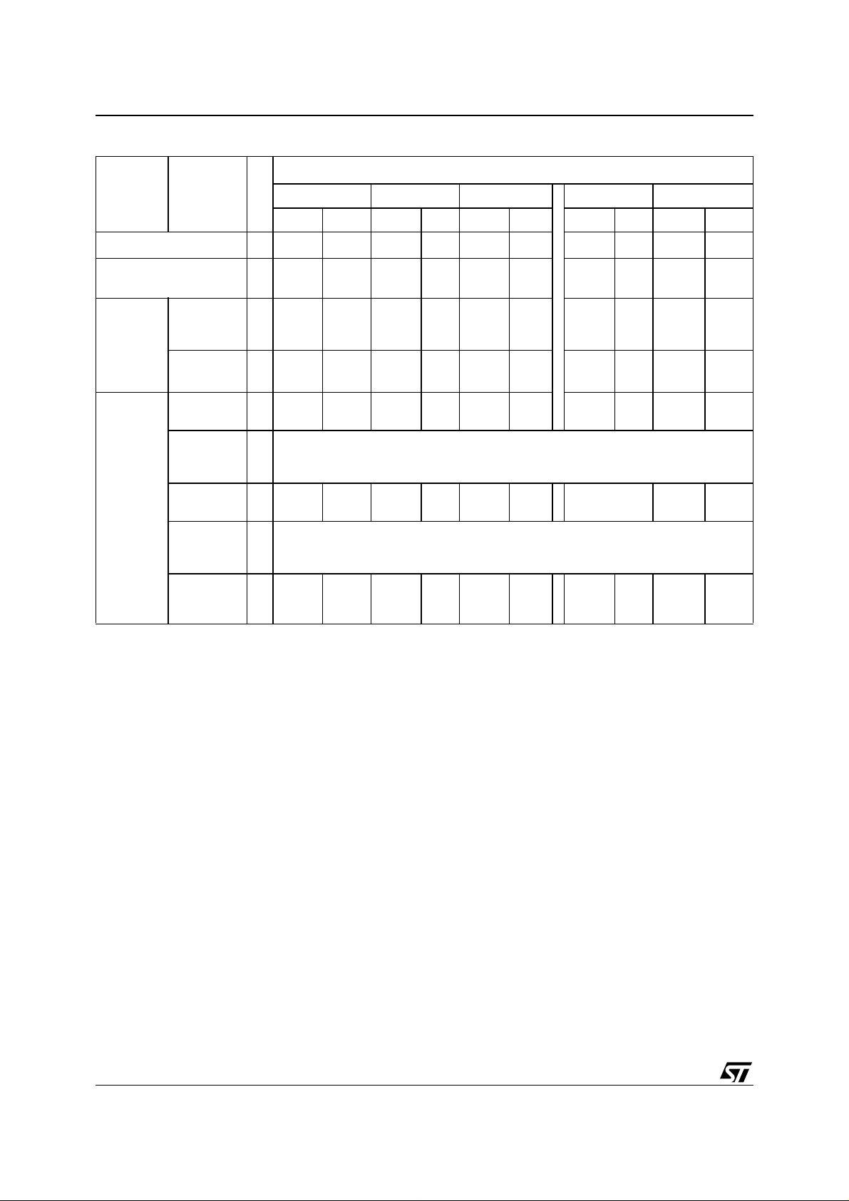
M36WT864TF, M36WT864BF
Table 7. Flash Factory Program Comman ds
Bus Write Operations
Command Phase
Cycles
(4)
Double Word Program
Quadruple Word
Program
(5)
Enhanced
Factory
Setup,
Program
3 BKA 35h WA1 PD1 WA2 PD2
5
2
+n+1BKA 30h BA D0h
Program
(6)
Verify, Exit
Setup,
first Load
n
+1
5
First
Quadruple
Enhanced
Factory
Program
(5,6)
Program &
Verify
Subsequent
Loads
Subsequent
Program &
Automatic
4
Automatic
Verify
Exit 1
Note: 1. WA=Word Addres s in t arget ed bank, BKA= Bank A d dress, P D=Pro gram Data , B A =Block Address .
2. WA1 is the Start Address. NOT WA1 is any address that is not in the sam e bl ock as W A1.
3. Address ca n remain Start i ng Address WA1 or be incremented.
4. Word Addresses 1 and 2 mus t be consecuti ve Addresses differing only for A0.
5. Word Addresses 1,2,3 and 4 m ust be consecutive Addresses dif fe ri ng only for A0 and A1.
6. A Bus Read m ust b e d one bet we en eac h Wr ite cyc le where t he da t a is p rog ra mmed or verif ied to rea d the St atus Reg ist er an d
check that the memory is ready to accept the next data. n = number of Wo rds, i = number of Pages to be programmed .
7. Address is o nly che ck ed for the fir st Wo rd o f each Page a s the o rder t o pro gram the Wo rds i n each pag e is fixe d so subs equent
Words in each Page can be written to any address.
1st 2nd 3rd Final -1 Final
Add Data Add Data Add Data Add Data Add D ata
BKA 56h WA1 PD1 WA2 PD2 WA3 PD3 WA4 PD4
NOT
WA1
NOT
WA1
WA4
WA4i
(7)
(2)
WA1
BKA 75h
WA1i
(2)
PD1
PD1i
WA2
WA1
WA2i
(7)
(3)
(2)
PD2
PD1
PD2i
WA1
WA3
WA2
WA3i
(7)
(2)
(3)
(7)
PD1
PD3
PD2
PD3i
WAn
WAn
WA3
(3)
(3)
(7)
PAn
PAn
PD3
NOT
WA1
FFFFh
(2)
(2)
(2)
(7)
FFFFh
FFFFh
PD4
PD4i
26/92

FLASH STATUS REGISTER
The Flash memory contains a Status Register
which provides information on the current or previous Program or Erase operations. Issue a Read
Status Register command to read the contents of
the Status Register, refer to Read Status Register
Command section for more details. To output the
contents, the Status Register is latched and updated on the falling edge of the Chip Enable or Output
Enable signals and can be read until Chip Enable
or Output Enable returns t o V
. The Status Reg-
IH
ister can only be read using single asynchronous
or single synchronous reads. Bus Read operations from any address within the bank, always
read the Status Register during Program and
Erase operations.
The various bits convey information about the status and any errors of the operation. Bits SR7, SR6,
SR2 and SR0 give information on the status of the
device and are set and reset by the device. Bits
SR5, SR4, SR3 and SR1 give inform ation on errors, they are set by the device but must be reset
by issuing a Clear Status Register command or a
hardware reset. If an error bit is set to ‘1’ the Status
Register should be reset before issuing another
command. SR7 to SR1 refer to the status of the
device while SR0 refers to the status of the addressed bank.
The bits in the Status Register are summarized in
Table 8, Status Register Bits. Refer to Table 8 in
conjunction with the following text descriptions.
Program/Erase Controller Status Bit (SR7).
The Program/Erase Controller Status bit indicates
whether the Program/Erase Con troller is active or
inactive in any bank. When the Program/Erase
Controller Status bit is Low (set to ‘0’), the Program/Erase Controller is active; when the bit is
High (set to ‘1’), the Program/Erase Controller is
inactive, and the device is ready to process a new
command.
The Program/Erase Controller Status is Low immediately after a Program/Erase Suspend command is issued until the Program/Erase Controller
pauses. After the Program/Erase Controller pauses the bit is High.
During Program, Erase, operations the Program/
Erase Controller Status bit can be polled to find the
end of the operation. Other bits in the Status Register should not be tested until the Program/Erase
Controller completes the operation and the bit is
High.
After the Program/Erase Cont roller completes its
operation the Erase Status, Program Status, V
PPF
Status and Block Lock Status bits should be tested
for errors.
Erase Suspend Status Bit (SR6). The Erase
Suspend Status bit indicates that an Erase opera-
M36WT864TF, M36WT864BF
tion has been suspended or is going to be suspended in the addressed block. When the Eras e
Suspend Status bit is High (set to ‘1’), a Program/
Erase Suspend command has been issued and
the memory is waiting for a Program/Erase Resume command.
The Erase Suspend Status should only be considered valid when the Program/Erase Controller Status bit is High (Program/Erase Controller inactive).
SR7 is set within the Erase Suspend Latency time
of the Program/Erase Suspend command being
issued therefore the memory may still complete
the operation rather than entering the Suspend
mode.
When a Program/Erase Re sume command is issued the Erase Suspend Status bit returns Low.
Erase Status Bit (SR5). The Erase Status bit
can be used to identify if the memory has failed to
verify that the block or bank has erased correctly.
When the Erase Status b it is High (set to ‘1’), the
Program/Erase Controller has applied the maximum number of pulses to the block or bank and
still failed to verify that it has erased correctly. The
Erase Status bit should be read once the Program/
Erase Controller Status bit is High (Program/Erase
Controller inactive).
Once set High, the Erase Status bit can only be reset Low by a Clear Status Register command or a
hardware reset. If set High it should be reset before a new Program or Erase command is issued,
otherwise the new command will appear to fail.
Program Status Bit (SR4). The Program Status
bit is used to identify a Program f ailure. Wh en t he
Program Status bit is High (set to ‘1’), the Program/Erase Controller has applied the maximum
number of pulses to the byte and still failed to verify that it has programmed correctly. The Program
Status bit should be read once the Program/Erase
Controller Status bit is High (Program/Erase Controller inactive).
Once set High, the Program Status bit can only be
reset Low by a Clear Status Register command or
a hardware reset. If set High it should be reset before a new command is issued, otherwise the new
command will appear to fail.
Status Bit (SR3). The V
V
PPF
be used to identify an invalid voltage o n the V
pin during Program and Erase operations. The
V
pin is only sampled at the beginning of a Pro-
PPF
gram or Erase operation. Indeterminate results
can occur if V
becomes invalid during an oper-
PPF
ation.
When the V
voltage on the V
voltage; when the V
‘1’), the V
Status bit is Low (set to ‘0’), the
PPF
pin has a voltage that is below the
PPF
pin was sampled at a valid
PPF
Status bit is High (set to
PPF
Status bit can
PPF
PPF
27/92

M36WT864TF, M36WT864BF
V
Lockout Voltage, V
PPF
tected and Program and Erase operations cannot
be performed.
Once set High, the V
PPF
set Low by a Clear Status Register command or a
hardware reset. If set High it should be reset before a new Program or Erase command is issued,
otherwise the new command will appear to fail.
Program Suspend Status Bit (SR2). The Program Suspend Status bit indicates that a Program
operation has been suspended in the addressed
block. When the Program Suspend Status bit is
High (set to ‘1’), a Program/Erase Suspend command has been issued and the memory is waiting
for a Program/Erase Resume command. The Program Suspend Status should only be considered
valid when the Program/Erase Controller Status
bit is High (Program/Erase Controller inactive).
SR2 is set within the Program Suspend Latency
time of the Program/Erase Suspend command being issued therefore the memory may still complete the operation rather than entering the
Suspend mode.
When a Program/Erase Re sume command is issued the Program Suspend Status bit returns Low.
Block Protection Status Bit (SR1). The Block
Protection Status bit can be used to identify if a
Program or Block Erase operation has tried to
modify the contents of a locked block.
When the Block Protection S tatus bit is High (set
to ‘1’), a Program or Erase operation has been attempted on a locked block.
, the memory is pro-
PPLK
Status bit can only be re-
Once set High, the Block Protection Status bit can
only be reset Low by a Clear Status Register command or a hardware reset. If set High it should be
reset before a new command is issued, otherwise
the new command will appear to fail.
Bank Wri te/Multiple Wor d Program Sta tus Bit
(SR0). The Bank Write Status bit indicates wheth-
er the addressed bank is programming or erasing.
In Enhanced Factory Program m ode the Multiple
Word Program bit shows if a Word has finished
programming or verifying depending on the phase.
The Bank Write Status bit should only be considered valid when the Pro gr a m/Erase Controller Status SR7 is Low (set to ‘0’).
When both the Pro gra m/Erase Controller Status bit
and the Bank Write Status bit are Low (set to ‘0’),
the addressed bank is executing a Program or
Erase operation. When the Program/Erase Controller Status bit is Low (set to ‘0’) and the Bank
Write Status bit is High (set to ‘1’), a Program or
Erase operation is being executed in a bank other
than the one being addressed.
In Enhanced Factory Program mode if Multiple
Word Program Status bit is Low (set to ‘0’), the device is ready for the next Word, if the Multiple Word
Program Status bit is High (set to ‘1’) the device is
not ready for the next Word.
Note: Refer to Appendix C, Flowcharts and Ps eudo Codes, for using the Status Register.
28/92
 Loading...