


32 Mbit (2Mb x16, Boot Block) Flash Memory
and 4 Mbit (256K x16) SRAM, Multiple Me mory Product
FEATURES SUMMARY
■ SUPPLY VOLTAGE
–V
–V
–V
■ ACCE SS TIME: 70,85ns
■ LOW POWE R CONSUMPT ION
■ ELECTRONIC SIGNATURE
– Manufacturer Code: 20h
– Top Device Code, M36W432T: 88BAh
– Bottom Device Code, M36W432B: 88BBh
FLASH MEMORY
■ 32 Mbit (2Mb x16) BOOT BLOCK
– 8 x 4 KWord Parameter Blocks (Top or
■ PROGRAMMING TIME
– 10µs typical
– Double Word Programming Option
■ BL OCK LOCKING
– All blocks locked at Power up
– Any combination of blocks can be locked
–WPF
■ AUTOMATIC STAND-BY MODE
■ PROGRAM and ERASE SUSPEND
■ COMMON FLASH INTERFACE
– 64 bit Security Code
■ SECURITY
– 64 bit user programmable OTP cells
– 64 bit unique device identifier
– One parameter block permanently lockable
=2.7Vto3.3V
DDF
DDS=VDDQF
= 12V for Fast Program (optional)
PPF
=2.7Vto3.3V
Bottom Location)
for Block Lock-Down
M36W432T
M36W432B
PRODUCT PREVIEW
SRAM
■ 4 Mbit (256K x 16 bit)
■ ACCE SS TIME: 70ns
■ LOW V
■ POWER DOWN FEATURES USING TWO
CHIP ENABLE INPUTS
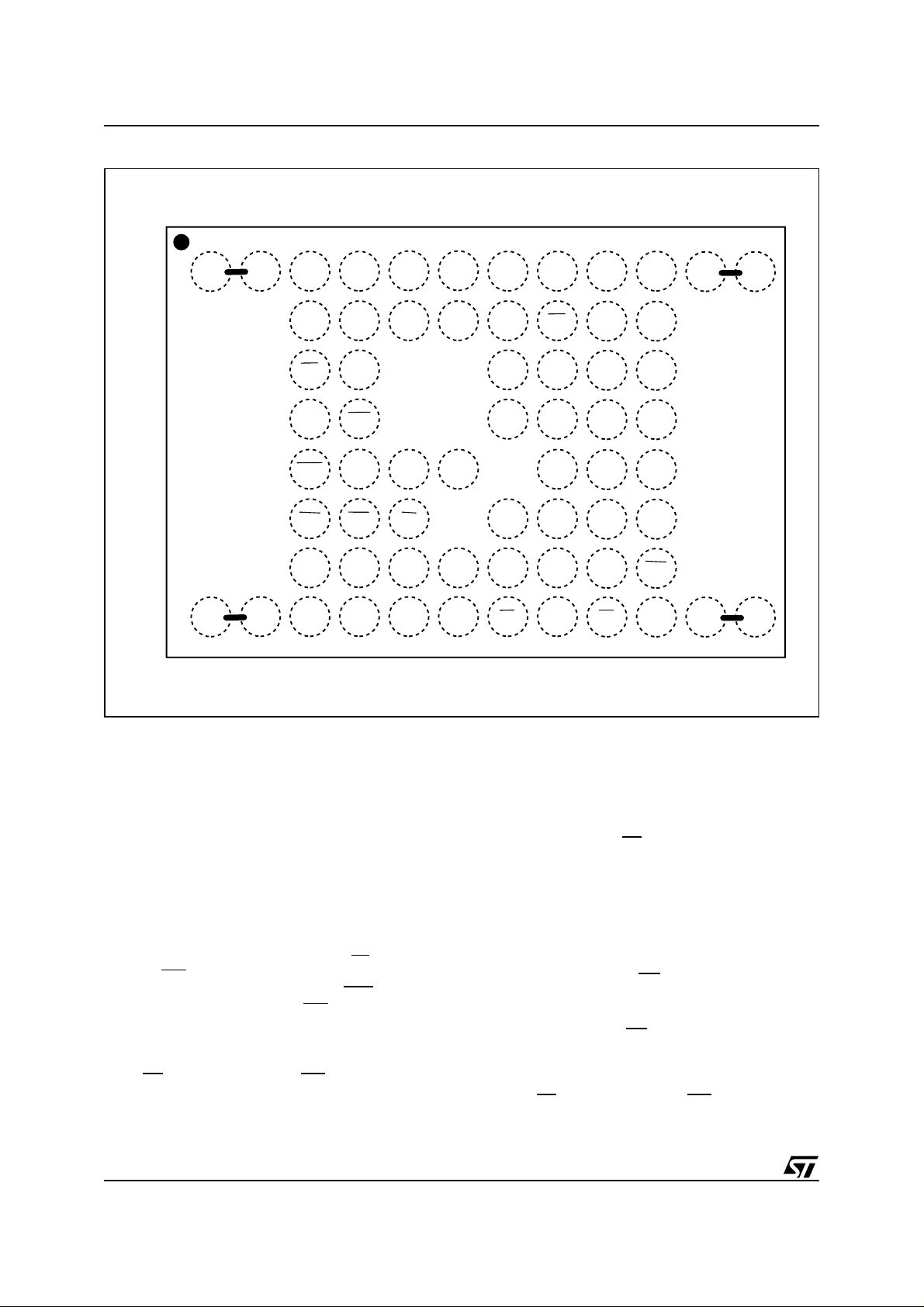
Figure 1. Packages
DATA RETENTION: 1.5V
DDS
FBGA
Stacked LFBGA66 (ZA)
8 x 8 ball array
February 2002
This is preliminary information on a new product now in development. Details are subject to change without notice.
1/57

M36W432T, M36W432B
TABLE OF CONTENTS
SUMMARYDESCRIPTION...........................................................5
Figure2.LogicDiagram ..........................................................5
Table 1. Signal Names . . . ........................................................5
Figure 3. LFBGA Connections (Top view through package). ..............................6
SIGNALDESCRIPTIONS............................................................6
FUNCTIONAL DESCRIPTION ........................................................8
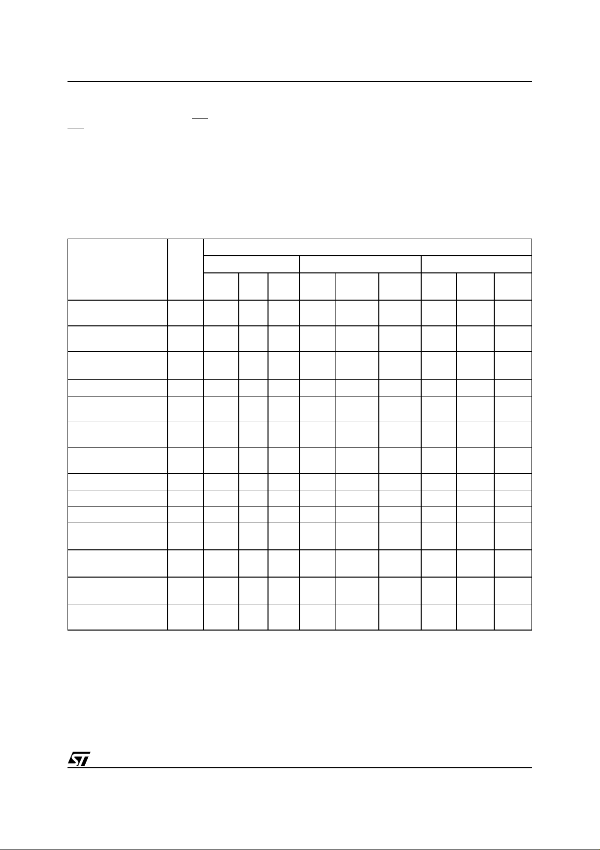
Figure 4. Functional Block Diagram .................................................8
Table2.MainOperationModes ....................................................9
FlashMemoryComponent......................................................10
Figure5.FlashBlockAddresses...................................................11
Figure6.FlashSecurityBlockMemoryMap..........................................11
SRAMComponent.............................................................11
OPERATINGMODES..............................................................12
FlashBusOperations..........................................................12
FlashCommandInterface.......................................................12
Table3.Commands ............................................................15
Table4.ReadElectronicSignature.................................................16
Table5.ReadBlockSignature....................................................16
Table6.ReadProtectionRegisterandLockRegister ..................................16
Table7.Program,EraseTimesandProgram/EraseEnduranceCycles ....................17
FlashBlockLocking...........................................................17
Table8.BlockLockStatus .......................................................18
Table9.LockStatus............................................................18
FlashStatusRegister ...........................................................19
Table10.StatusRegisterBits.....................................................20
SRAMOperations .............................................................20
MAXIMUMRATING................................................................21
Table11.AbsoluteMaximumRatings...............................................21
DCandACPARAMETERS .........................................................22
Table 12. Operating and AC Measurement Conditions..................................22
Figure7.ACMeasurementI/OWaveform...........................................22
Figure 8. AC Measurement Load Circuit. . . ..........................................22
Table 13. Device Capacitance.....................................................22
Table14.DCCharacteristics......................................................23
Figure9.FlashReadACWaveforms...............................................24
Table15.FlashReadACCharacteristics............................................24
2/57

M36W432T, M36W432B
Figure10.FlashWriteACWaveforms,WriteEnableControlled..........................26
Table16.FlashWriteACCharacteristics,WriteEnableControlled........................27
Figure 11. Flash Write AC Waveforms, Chip Enable Controlled...........................28
Table 17. Flash Write AC Characteristics, Chip Enable Controlled. . .......................29
Figure12.FlashPower-UpandResetACWaveforms..................................30
Table18.FlashPower-UpandResetACCharacteristics................................30
Figure 13. SRAM Read AC Waveforms, Address Controlled with UBS = LBS = V
Figure14.SRAMReadACWaveforms,E1S,E2SorGSControlled.......................31
Figure 15. SRAM Standby AC Waveforms . ..........................................32
Table19.SRAMReadACCharacteristics...........................................32
Figure16.SRAMWriteACWaveforms,WSControlledwithGSLow ......................33
Figure17.SRAMWriteACWaveforms,WSControlledwithGSHigh......................33
Figure18.SRAMWriteACWaveforms,UBSandLBSControlled.........................34
Figure19.SRAMWriteACWaveforms,E1SControlled ................................34
Table20.SRAMWriteACCharacteristics ...........................................35
Figure 20. SRAM Low V
Figure 21. SRAM Low V
Table 21. SRAM Low V
DataRetentionACWaveforms,E1SControlled................36
DDS
DataRetentionACWaveforms,E2SControlled................36
DDS
DataRetentionCharacteristic...............................36
DDS
PACKAGE MECHANICAL . . . .......................................................37
...........31
IL
Figure22.StackedLFBGA66-8x8ballarray,0.8mmpitch,BottomViewPackageOutline....37
Table 22. Stacked LFBGA66 - 8 x 8 ball array, 0.8 mm pitch, Package Mechanical Data . . . ....37
Figure 23. Stacked LFBGA66 Daisy Chain - Package Connections (Top view through pack age) . 38
Figure 24. Stacked LFBGA66 Daisy Chain - PCB Connections proposal (Top view through package)39
PARTNUMBERING ...............................................................40
Table23.OrderingInformationScheme.............................................40
Table24.DaisyChainOrderingScheme ............................................40
REVISIONHISTORY...............................................................41
Table25.DocumentRevisionHistory...............................................41
APPENDIXA.FLASHMEMORYBLOCKADDRESSTABLES .............................42
Table 26. Top Boot Block Addresses, M36W432T . ....................................42
Table27.BottomBootBlockAddresses,M36W432B ..................................43
APPENDIXB.COMMONFLASHINTERFACE(CFI) .....................................44
Table28.QueryStructureOverview................................................44
Table 29. CFI Query Identification String . . ..........................................44
Table30.CFIQuerySystemInterfaceInformation.....................................45
Table31.DeviceGeometryDefinition...............................................46
Table 32. Primary Algorithm-Specific Extended Query Table .............................47
Table33.SecurityCodeArea.....................................................48
APPENDIXC.FLASHMEMORYFLOWCHARTSandPSEUDOCODES.....................49
3/57

M36W432T, M36W432B
Figure 25. Program Flowchart and Pseudo Code . . ....................................49
Figure 26. Double Word Program Flowchart and Pseudo Code ...........................50
Figure 27. Program Suspend & Resume Flowchart and Pseudo Code .....................51
Figure 28. Erase Flowchart and Pseudo Code ........................................52
Figure 29. Erase Suspend & Resume Flowchart and Pseudo Code. .......................53
Figure 30. Locking Operations Flowchart and Pseudo Code .............................54
APPENDIX D. FLASH MEMORY COMMAND INTERFACE and PROGRAM/ERASE CONTROLLER
STATE..........................................................................55
Table34.WriteStateMachineCurrent/Next,sheet1of2...............................55
Table35.WriteStateMachineCurrent/Next,sheet2of2...............................56
4/57
SUMMARY DESCRIPTION
The M36W432 is a low voltage M ultiple Memory
Product which combines two memory devices; a
32 Mbit boot block F lash memory and a 4 Mbit
SRAM. Rec ommended operating condit ions do
not allow both the Flash and the SRAM to be active at the same time.
The memory is offered ina StackedLFBGA66 (0.8
mm pitch) pack age and is supplied wi th all the bits
erased (set to ‘1’).
M36W432T, M36W432B
Table 1. Signal Names
A0-A17 Address Inputs
A18-A20 Address Inputs for Flash Chip only
DQ0-DQ15 Data Input/Output
V
V
DDF
DDQF
Flash Power Supply
Flash Power Supply for I/O Buffers
Figure 2. Logic Diagram
V
DDQF
V
M36W432T
M36W432B
A0-A20
EF
GF
WF
RPF
WPF
E1S
E2S
GS
WS
UBS
LBS
21
V
DDF
PPF
V
DDS
16
DQ0-DQ15
V
PPF
V
SSF
V
DDS
V
SSS
NC Not Connected Internally
Flash control functions
EF
GF
WF
RPF
WPF
SRAM control functions
, E2S Chip Enable inputs
E1S
GS
WS
UBS
LBS
Flash Optional Supply Voltage for Fast
Program & Erase
Flash Ground
SRAM Power Supply
SRAM Ground
Chip Enable input
Output Enable input
Write Enable input
Reset input
Write Protect input
Output Enable input
Write Enable input
Upper Byte Enable input
Lower Byte Enable input
V
SSF
V
SSS
AI05200
5/57
M36W432T, M36W432B
Figure 3. LFBGA Connections (Top view throu gh p ackage)
654321#2#1
A
B
C
D
E
F
G
H
NC
NC
A8 A10
RPF
SSS
V
PPF
UBS
A17
NC V
A5
A15 A14
DQ11A19WPF
A13A11A20NC
DQ9GSLBS
EFA0A4NC
A12
WSDQ15A9A16
DQ6DQ13NCWF
E2SDQ12V
DQ10
DQ8
A2A3A6A7A18
SSF
V
SSFVDDQF
DQ14
DQ4
V
DDS
DQ7
DQ5
V
DQ3DQ2
DQ1DQ0
E1SA1
DDF
NCNCGF
#4#387
NCNC
NC
SIGNAL DESCRIPTIONS
See Figure 2 Logic Diagram and Table 1,Signal
Names, for abrief overview of the signals connected to this device.
Address Inputs (A0-A17). Addresses A0-A17
are common inputs for the Flash an d the SRAM
components. The Address Inputs select the cells
in the mem ory array to acces s during Bus Read
operations. During Bus Write operations they control thecommands sent to the Command Interface
ofthe internalstate machine.The Flashmemory is
accessed through the Chip Enable (
Enable (WF
) signals, while the SRAM is accessed
through two Chip Enab le signals (E1S
and the Write Enable signal (WS
EF)andWrite
and E2S)
).
Address Inputs (A18-A20). A ddres s es A18-A20
are in puts for the Flash component only. The
Flash memory is acces s ed through the Chip Enable (EF
) and Write Enable (WF) signals
Data Input/Output (DQ0-DQ15). The Data I/O
outputs the data stored at t he s elected address
AI05201
during a Bus Read operationor inputsa command
orthedatatobeprogrammedduringaWriteBus
operation.
Flash Chip Enable (EF
). The Chip En able input
activates the Flash memory control logic, input
buffers, decoders and sense amplifiers. When
Chip Enable is at V
is in active mode. When Chip Enable is at V
andResetisatVIHthe device
IL
the
IH
memory is deselected,the outputsare high impedance an d the power consumption isreduced tothe
standby level.
Flash Output Enable (GF
). The Output Enable
controls the data outputs during the Bus R ead operation of the Flash memory.
Flash Write Enable (
WF). The Write Enable
controls the Bus Write operation of the Flash
memory’s Command Interface. The data and address inputs are latched on the rising edge of Chip
Enable, EF
, or Write Enable, WF, whichever oc-
curs first.
6/57

M36W432T, M36W432B
Flash Write Protect (WPF). Write Protect is an
input that gives an additional hardware protection
for each block. When Write Protect is at V
,the
IL
Lock-Down is enabled and the protection status of
the block cannot be changed. When Write Protect
is at V
, the Lock-Down is disabled and the block
IH
can be locked or unlocked. (refer to Table 6, Read
Protection Registerand Protection Register Lock).
Flash Reset (RPF
). The Res et input provides a
hardware reset of the Flash memory. When Res et
is at V
, the m emory is in reset mode: the outputs
IL
are high impedance and the c urrent consumption
is minimized. After R es et all blocks are i n the
Locked state. When Reset is at V
, the device is
IH
in norm al operation. Exiting resetmode the device
enters read array mode, but a negative transition
of Chip Enable or a change of the address is required to ensure valid data outputs.
SRAM Chip Enable (E1S
,E2S). TheChipEn-
able inputs activate the SRAM memory control
logic, input buffers and decoders. E1S
E2S at V
deselects the memory and reduces the
IL
power consumption to the standby level. E1S
at VIHor
and
E2S can also be used to control writing to the
SRAM memory array, while WS
is not allowed to set EF
at V
at the same time.
IH
at V
SRAMWriteEnable(WS
remains at V
E1S at VILandE2S
IL,
IL.
). The Write Enable in-
put cont rols writing to the SR AM memory array.
is active low.
WS
SRAM Output Enable (GS)
. The Ou tput Enable
gates the outputs through the data buffers during
a read operation of the SRAM memory. GS
is ac-
tive low.
SRAM Upper Byte Enable (UBS)
. The Upper
Byte Enable enables the upper bytes for SRAM
(DQ8-DQ15). UBS
SRAM Lower Byte Enable (LBS
is active low.
). The Lower
Byte Enable enables t he lower bytes for SRAM
(DQ0-DQ7). LBS
is active low.
V
Supply Voltage (2.7V to 3.3V). V
DDF
vides the power supply to the internal core of the
Flash Memory device. It is the main power supply
for all operations (Read, Program and Erase).
V
V
and V
DDQF
provides the power supply for the Flash
DDQF
memory I/O pins and V
Supply Voltage (2.7V to 3.3V).
DDS
provides the power
DDS
supply for the SRAM control pins. This allows all
Outputs to be powered independently from the
Flash core power supply,V
to V
DDS
V
Program Supply Voltage. V
PPF
DDF.VDDQF
control input and a power supply pin for the Flash
memory. The two functions are s elect ed by the
voltage range applied to the pin. The S upply Voltage V
and the Program Supply Voltage V
DDF
can be applied in any order.
If V
V
age lower than V
against program or erase, while V
is kept in a low voltage range (0V to 3.6V)
PPF
is seen as a control input. In this case a volt-
PPF
gives anabsolute protection
PPLK
PPF>VPPLK
ables these functions (see Table 14, DC Charac teristics for the rele va nt values ). V
sampled at the beginning of a program or erase; a
It
change in its value after the operation has started
does not haveany effect and programor eraseoperations continue.
If V
is in the range 11.4V to 12.6V it acts as a
PPF
power supply pin. In this condition V
stable until the Program/Erase algorithm is completed (see Table 16 and 17).
V
SSF
and V
Ground. V
SSS
SSF
and V
ground reference for all voltage measurements in
the Flash and SRAM chips, respectively.
Note: E ach device in a system should have V
DF
,V
DDQF
and V
decoupled with a 0.1µF ca-
PPF
pacitor clos e to the pin. See Figure 9, AC
Measurement Load Circuit. The PCB trace
widths should be sufficient to carry the required V
program and erase currents.
PPF
DDF
canbetied
is both a
PPF
PPF
must be
PPF
SSS
pro-
PPF
en-
is only
are the
D-
7/57
M36W432T, M36W432B
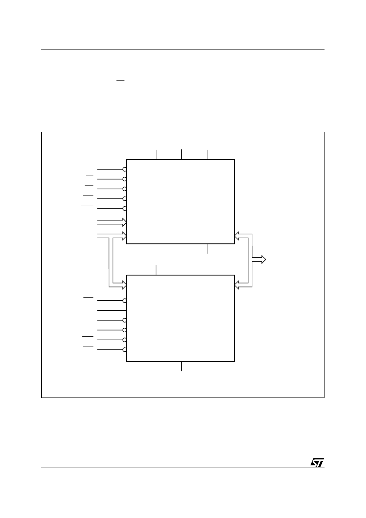
FUNCTIONAL DESCRIPTION
The Flash and SRAM components have separate
power supplies and grounds and are distinguished
by three chip ena ble inputs: EF
ory and, E1S
and E2S for the SRAM.
Recommended operating conditions do not allow
both theFlash and the SRAM to be in active mode
at the same time. The mos t common example is
Figure 4. Functional Block Diagram
for the Flash mem-
simultaneous rea d operations on the Flash and
the SRAM which would result in a data bus contention. Therefore it is recommended to put the
SRAM in the high impedance state when reading
theFlashandviceversa(seeTable2MainOperation Modes for details).
EF
EF
GF
GF
WF
WF
RPF
RPF
WPF
WPF
A18-A20
A18-A20
A0-A17
A0-A17
E1S
E1S
E2S
E2S
GS
GS
WS
WS
UBS
UBS
LBS
LBS
V
DDF
V
DDF
Flash Memory
Flash Memory
32 Mbit (x16)
32 Mbit (x16)
V
DDS
V
DDS
V
DDQF
V
DDQF
SRAM
SRAM
4 Mbit (x16)
4 Mbit (x16)
V
V
V
V
PPF
PPF
SSF
SSF
DQ0-DQ15
DQ0-DQ15
8/57
V
V
SSS
SSS
AI05202
AI05202
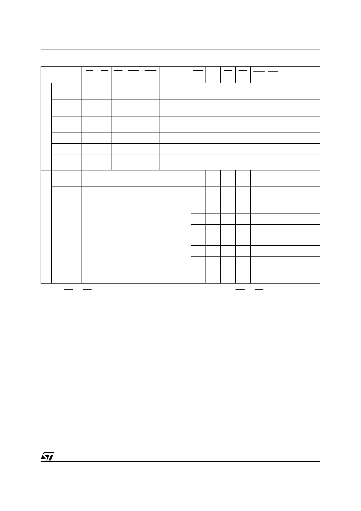
Table 2. Main Operation Modes
Operation
Mode
Read
Write
Block
Locking
Standby
Flash Memory
Reset X X X
Output
Disable
Read Flash must be disabled
Write Flash must be disabled
Standby/
Power
Down
SRAM
Data
Retention
Output
Disable
Note: X = VILor VIH,V
1. If UBS
and LBS are tied together the bus is at 16 bit. For an 8 bit bus configuration use UBS and LBS separately.
GF WF RPF WPF
EF
V
ILVILVIHVIH
V
ILVIHVILVIH
V
IL
V
IH
XX
XX
V
V
V
V
ILVIHVIHVIH
Any Flash mode is allowable
Any Flash mode is allowable
Any Flash mode is allowable
=12V±5%.
PPFH
M36W432T, M36W432B
V
PPF
X Don't care SRAM must be disabled
V
V
IH
V
IH
IL
X Don't care Any SRAM mode is allowed Hi-Z
IH
X Don't care Any SRAM mode is allowed Hi-Z
IL
DDF
V
PPFH
Don't care SRAM must be disabled X
X Don't care Any SRAM mode is allowed Hi-Z
E1S E2S GS WS
or
SRAM must be disabled Data Input
V
ILVIHVILVIH
V
ILVIHVIHVIL
V
XXX X Hi-Z
IH
V
X
IL
XXXX
V
XXX X Hi-Z
IH
V
X
IL
XXXX
V
ILVIHVIHVIH
UBS,LBS
V
IL
V
IL
X X X Hi-Z
V
IH
X X X Hi-Z
V
IH
X Hi-Z
(1)
DQ15-DQ0
Data
Output
Data out
Word Read
Data in
Word Write
Hi-Z
Hi-Z
9/57

M36W432T, M36W432B
Flash Memory Component
TheFlashMemoryisa32Mbit(2Mbitx16)device that can be erased electrically at th e block
level and progra m m ed in-system on a Word-byWord basis. These operations can be performed
using a single low voltage (2.7 to 3.3V) supply
and t he V
same voltage range. An optional 12V V
for de vice I/0operation feature the
DDQF
PPF
power
supply is provided to speed up customer programming.
The dev ice features an asymmetrical blocked architecture with an array of 71 blocks: 8 Parameter
Blocksof4KWordand63MainBlocksof32
KWord. The M36W432T device has the Flash
Memory Parameter Blocks at the top of the memoryaddress spacewhile theM36W432B devicelocates the Parameter Blocks s tarting from the
bottom. The memory m aps are shown in Figure 5,
Block Addresses.
The Flash Memory features an instant, individual
block locking scheme that allows any block to be
locked or unlocked with no latency, enabling instant code and data protection. All blocks have
three levels of protection. They can be lock ed and
locked-down individually preventing any accidental programming or erasure. There is an additional
hardware protection against program and erase.
When V
PPF
≤ V
all blocks are protected
PPLK
against program or erase. All blocks are locked at
Power Up.
Each block can be erased separately. Erase can
be suspended in order to perform either read or
program in any other block and then resumed.
Program can be suspended to read data in any
other block and then resumed. Each block can be
programmed and erased over 100,000 cycles.
The device includes a 128 bit Protec tion Register
and a Securit y Block to increase the prote ction of
a system design. The Protection Register is divided into two 64 bit segments, the first one contains
a unique device number written by ST, whi le the
second one is one-time-programmable by the user. The user programmable segment can be permanently protected. The Sec urity Block,
parameter block 0, can be permanently p ro tected
by the user. Figure 6, shows the Flash Security
Block Memory Map.
Program a nd Erase commands are written to the
Command Interface of the memory. An on-c hip
Program/Erase Control ler takes care of the timings necessary for program and erase operations.
The end of a program or erase operation can be
detected and any error conditions identified. The
command set required to control the memory is
consistent with JEDEC standards.
10/57
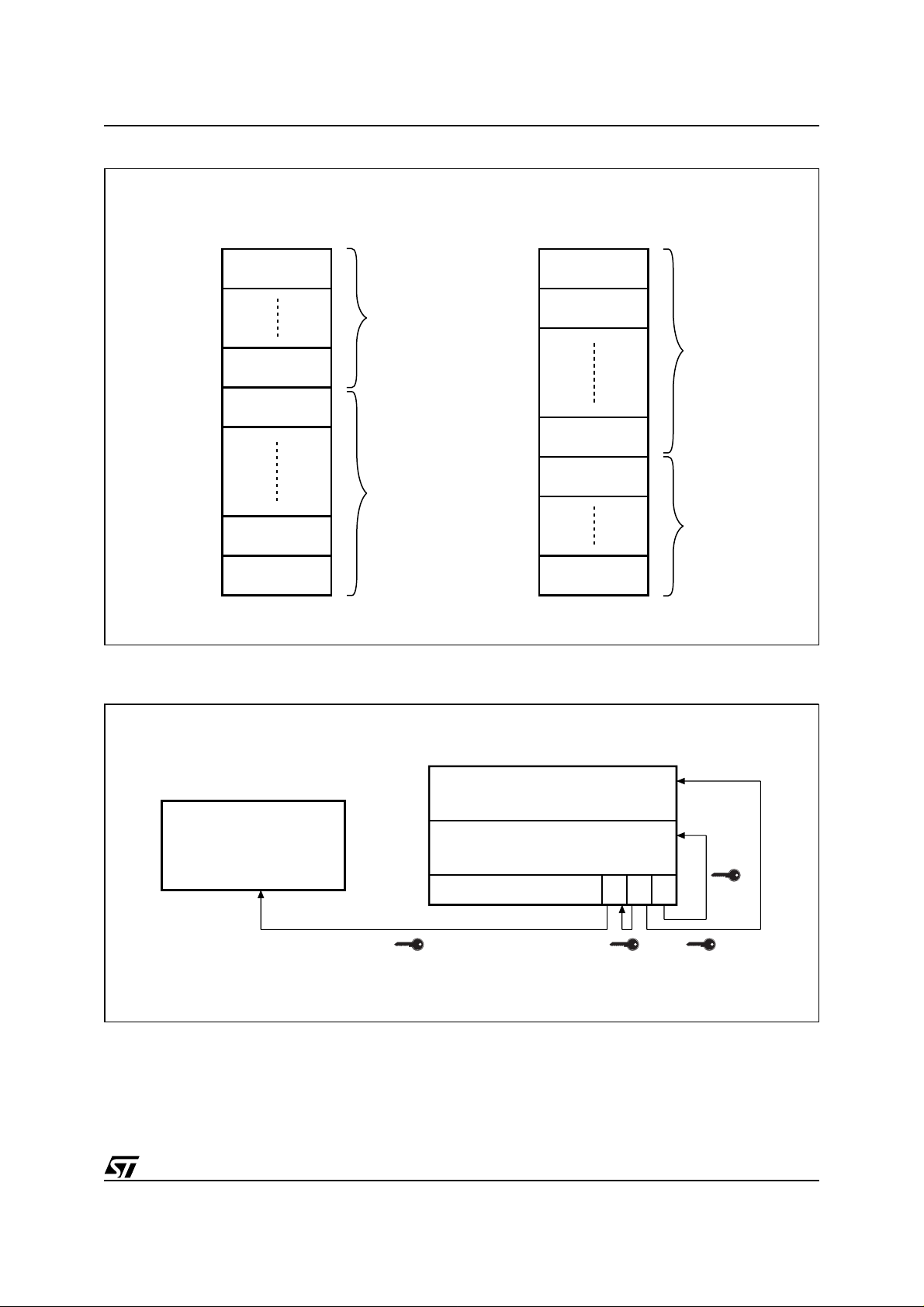
Figure 5. Flash Block Addresses
M36W432T, M36W432B
Top Boot Block Addresses
1FFFFF
1FF000
1F8FFF
1F8000
1F7FFF
1F0000
00FFFF
008000
007FFF
000000
Note: Also see Appendix A, Tables 26 and 27 for a full listing of the Flash Block Addresses.
4 KWords
Total of 8
4 KWord Blocks
4 KWords
32 KWords
Total of 63
32 KWord Blocks
32 KWords
32 KWords
Bottom Boot Block Addresses
1FFFFF
1F8000
1F7FFF
1F0000
00FFFF
008000
007FFF
007000
000FFF
000000
32 KWords
32 KWords
Total of 63
32 KWord Blocks
32 KWords
4 KWords
Total of 8
4 KWord Blocks
4 KWords
AI05203
Figure 6. Flash Security Block Memory Map
88h
85h
84h
Parameter Block # 0
81h
80h
SRAM Component
The SRAM is an 4 Mbit asynchronous random access mem ory which features a super low voltage
operation and low current consumption withan ac -
User Programmable OTP
Unique device number
Protection Register Lock 2 1 0
AI05204
cess time of 70 ns in all conditions. The memory
operations can be performed using a single low
voltage supply, 2.7V to 3.3V, whic h is the same as
the Flash voltage supply.
11/57

M36W432T, M36W432B
OPERATING MODES
Flash Bus Operations
There are six stand ard bus operations that control
the device. These are B us Read, Bus Write, Ou tput Disable, Standby, Automatic Standby and Reset. See Table 2, Main Operation Modes, for a
summary.
Typically glitches of less than 5ns on Chip Enable
or Write Enable are ignored by the memory and do
not affect bus operations.
Read. Read Bus operations are used to output
the contents of the Memory Array, the Electronic
Signature, the Status Register and the Comm on
Flash Interface. Both Chip Enable and Output EnablemustbeatV
in order to perform a read op-
IL
eration. The Chip Enable input should be used to
enable the device. Output Enable should be used
to gate data onto the output. The data read depends on the previous command written to the
memory (see Command Interface section). See
Figure 9, Read Mode AC Waveforms , and Table
15, Flash Read AC Cha r acteristics, for details of
when the output becomes valid.
Read mode isthe default state of the device when
exiting Reset or after power-up.
Write. B us Write operations write Commands to
the memory orlatch InputData to beprogrammed.
A write operation is initiated when Chip Enable
and Write Enable are at V
V
. Commands, Input Data and Addresses are
IH
with Output Enable at
IL
latched on the rising edge of Write Enable or Chip
Enable, whichever occurs first.
See Figures 10 and 11, Write AC Waveforms, and
Tables 16 and 17, Flash Write AC Chara cteristics,
for details of the timing requirements.
Output Disable. The data ou tpu ts are high im pedance when the Output Enable is at V
.
IH
Standby. Standby disables most o f the internal
circuitryallowing asubstantial reduc t ion ofthe current consumption. The memory is in stand-by
when Chip Enable is at V
andthedeviceisin
IH
read mode. The power consumption is reduced to
the stand-by level and the outputs are set to high
impedance, independently f rom the Output Enable
or Write Enable inputs. If Chip Enable switches to
during a program or erase operat ion, the de-
V
IH
vice enters Standby mode when finished.
Automatic Standby. Automatic Standby pro-
vides a low power consumption state during Read
mode. Following a read operation, the device enters Automatic Standby after 150ns of bus inactivity even if Chip Enable is Low, V
current is reduced to I
. The data I nputs/Out-
DD1
, and the supply
IL
puts will s till output data if abus Read operation is
in progress.
Reset. During Reset mode when O ut put Enable
is Low, V
, the memory is des elected and the out-
IL
puts are high impedance. The memory is in R eset
mode when Reset is at V
. The power consump-
IL
tion is reduced to the Standby level, independently
from the Chip Enable, Output Enable or Write Enable inputs. If Reset ispulled to V
during aPro-
SSF
gram or Erase, this operation is aborted and the
memory content is no longer valid.
Flash Command Interface
All Bus Write operations to the memory are interpreted by the Command Interface. Commands
consist of one or more sequential Bus Write operations. An internal Program/Erase Controller handles a ll timings and verifies the correct execution
of the Program and Erase commands. The Pr ogram/Erase Controller provides a Status Register
whose output may be read at any time during, to
monitor the progress of the operation, or the Program/Erase states. See Appendix 29, Table 34,
Write State Machine Current/Next, for a summary
of the Command Interface.
The Command Interface is res et to Read mode
when power is f irst applied, when exiting from Reset or whenever V
is lower than V
DDF
LKO
.Command sequences must be followed exactly. Any
invalid combination of com mands will reset the device to Read mode. Refer to Table 3, Commands,
in conjunction with the text descriptions below.
Read Memory Ar ray Command. The Read
command returns the memory to its Read mode.
One Bus Write cycle is required to issue t he Read
Memory Array command and returnthe memory to
Read mode. Subsequent read operations willread
the addressed location and output the data. When
a device Reset occurs, the memory defaults to
Read mode.
Read Status Register Command. The Status
Register indicates when a program or eras e operation is complete and the success or failure of the
operation itself. Issue a Read Status Register
command to read the Status Register’s contents.
Subsequent Bus Read operations read the Status
Register at any address, untilanother command is
issued. See Table 10, S tatus Register Bits, for details on the definitions of the bits.
The R ead Status Register command may be issued at any time , even during a Program/Erase
operation. Any Read atte mpt during a Program/
Erase operation will automatically output the content of the Status Register.
12/57

M36W432T, M36W432B
Read Electronic Signature Command. The
Read Electronic Signature command reads the
Manufacturer and Dev ice Codes and the Block
Locking Status, or the Protection Register.
The Read Electronic Signature command consists
of one write cycle, a subsequent read will output
the Manufacturer Code, the Device Code, the
Block Lock and Lock-Down Status, o r t he Protection and Lock R egister. See Tables 4, 5 and 6 for
the valid address.
Read CFI Query Command. The Read Query
Command is used to read data from the Common
Flash Interface (CFI) Memory Area , allowing programming equipment or applications to automatically match their interface to the characteristics of
thedevice.OneBusWritecycleisrequiredtoissue the Read Query C ommand. Once the command is issued subsequent Bus Read operations
read from the Common Flash Interface Memory
Area. See Appendix B, Common Flash Interface,
Tables 28, 29, 30, 31, 32 and 33 f or details on the
information contained in the Common Flash Interface memory area.
Block Erase Command. TheBlockErasecommandcanbeusedtoeraseablock.Itsetsallthe
bits within the selected block to ’1’. All previous
data in the block is lost. If the block is protected
then the Erase operat ion will abort, the data in the
block will not be changed and the Status Register
will output the error.
Two Bus Write cycles are required to issue the
command.
■ Th e first bus cycle s ets up the Erasecommand.
■ Th e second la tches the block address in the
internal state machine and starts the Program/
Erase Controller.
If the seco nd bus cycle is not Write Erase Confirm
(D0h), Status Register bits b4 and b5 are set and
the command aborts.
Erase abortsif Reset turns to V
. As data integrity
IL
cannot be guaranteed when the Erase operation is
aborted, the block must be erased again.
During Erase operations the memory will accept
the Read Status Register command and the Program/Erase Suspen d command, all other commands will be ignored. Typical Erase times are
given in Table 7, Program, E ras e Times and P r ogram/Erase Endurance Cycles.
See Appendix C, Figure 28, Erase Fl owc hart and
Pseudo Code, for a suggested flowchart fo r using
the Erase command.
Program Command. The memory array can be
programmed word-by-word. Two bus write cycles
are required to issue the Program Command.
■ Th e first bus cycle sets up the Program
command.
■ Th e secondlatchesthe Addres s andtheData to
be written and starts the Program/Erase
Controller.
During Program operations the memory will accept the Read Status Regist er command and the
Program/Erase S us pend command. Typical Program times are given in Table 7, Program, Erase
Times and Program/Erase Endurance Cycles.
Programming aborts if Reset goes to V
. As data
IL
integrity cannot be guaranteed when the program
operation is aborted , the block containing the
memory location must be erased and reprogrammed.
See Appendix C, Figure 25 , Program Flowchart
and Pseudo Code, for the flowchart for using the
Program command.
Double Word Program Command. This feature
is offered to improve the programming throughput,
writing a page of two adjacent words in parallel.The two words must differ only for the addres s
A0. Programming should n ot be attempted when
V
PPF
ed if V
is not at V
is below V
PPF
.The command canbeexecut-
PPH
but the res ult is not guar-
PPH
anteed.
Three bus write cycles are necessary to issue the
Double Word Program command.
■ Th e first bus cycle sets up the Double Word
Program Command.
■ The second bus cyclelatches the A ddress and
theDataofthefirstwordtobewritten.
■ The third bus cycle la tches the A ddres s and the
Data of thesecond wordto b e written and starts
the Program/Erase Controller.
Read operations output the Status Register content after the programming has started. Programming aborts if Reset goes to V
. As data integrity
IL
cannot be guaranteed when the program operation is aborted, the block containing the memory
location must be erased and reprogrammed.
See Appendix C, Figure 26, Double Word Program Flowchart and Pseudo Code, for the flowchart for using the Double Word Program
command.
Clear Status Register Command. The Clear
Status Register command can be used to reset
bits 1, 3, 4 and 5 in the Status Register to ‘0’. One
bus write cycle is required to issue the Clear Status Register command.
The bits in the Status Register do not automatically ret urn to ‘0’ when a new P rogram or Erase command is issued. The error bits in the Status
Register should be c leared before attempting a
new Program or Erase command.
13/57

M36W432T, M36W432B
Program/Erase Suspend Command. The Pro-
gram/Erase Suspend c ommand is u sed to pause
a Program orErase operation.One bus writecycle
is required t o issue the Program/Erase c ommand
and pause the Program/Erase controller.
During Program/Erase Suspend the Command Interface will accept the Program/Erase Resume,
Read Array, ReadStatus Register,Read Electronic Signature and Read CFI Query commands. Additionally, if the s uspend operation was Erase then
the Program, Block Lock, Block Lock-Down or
Protection Program commands will also be accepted. The block being erased may be protected
by issuing the B lock Protect, BlockLock or Protection Program commands. When the Program/
Erase Resume command is issued the operation
will complete. Only the blocks not being erased
may be read or programmed correctly.
During a Program/Erase Suspend, the device can
be placed in a pseudo-standby mode by taking
Chip Enable to V
Reset turns to V
. Program/Erase i s aborted if
IH
.
IL
See Appendix C, Figure 27, Program or Double
Word P rogram Suspend &Resume Flowchart and
Pseudo Code, and Figure 29, Erase Suspend &
Resume Flowchart and P s eudo Code for flowcharts for using theProgram/Erase Suspend command.
Program/Erase Resume Command. The Pro-
gram/Erase Resume command can be used torestart the Program/Erase Controller after a
Program/Erase Suspend operation has paused it.
One Bus Write cycle is required to issue the command. Once the command is issued subsequent
Bus Read operations read the Status Register.
See Appendix C, Figure 27, Program or Double
Word P rogram Suspend &Resume Flowchart and
Pseudo Code, and Figure 29, Erase Suspend &
Resume Flowchart and P s eudo Code for flowcharts for using the Program/Erase Resume command.
Protection Register Program Command. The
Protection Register Program command is used to
Program the 64 bit user One-Time-Programmable
(OTP) segment of the Protection Register. The
segment is programmed 16 bits at a time. When
shipped all bits in the segment are set to ‘1’. The
user can only program the bits to ‘0’.
Two write cycles are required to issue the Protection Register Program command.
■ Th e first bus cycle sets up the Protection
Register Program command.
■ Th e secondlatchesthe Addres s andtheData to
be written to the Protection Register and starts
the Program/Erase Controller.
Read operations output the Status Register content after the programming has started.
The segment can beprotected byprogramming bit
1 of the Protection Lock R egister. Bit 1 of t he Protection Lock Register protects bit 2 of t he Protection Lock Re gister. Programming b it 2 of the
Protection Lock Registerwill result in a permanent
protection of the Security Block (see Figure 6,
Flash Security Block Memory Map). Attempting to
program a previously protec t ed Protection Register wil l result in a Status Register error. The protection of the Protection Register and/or the
Security Block is not reversible.
The Protection Register Program cannot be suspended.
Block Lock Command. The Block Lock command is used to lock a block and prevent Pr ogram
or Erase operations from changing the data in it.
All blocks are locked at power-up or reset.
Two Bus Write cycles are required to issue the
Block Lock command.
■ Th e first bus cycle sets up the Block Lock
command.
■ The second Bus Write cycle latches the block
address.
The Lock Status can be monitored for each block
using the Read Block Signature command. Table.
9 shows the Lock Status afterissuing a Block Loc k
command.
The Block Lock bits are volatile, once set they remain set u ntil reset or power-down/power-up.
They are c leared by a Blocks Unlock command.
Refer to the section, Block Locking, for a detailed
explanation.
Block Unlock Command. The Blocks Unlock
command is used to unlock a block, allowing the
block to be programmed orerased. Two Bus Write
cycles are required to issue the Blocks Unlock
command.
■ Th e first bus cycle sets up the Block Unlock
command.
■ The second Bus Write cycle latches the block
address.
The Lock Status can be monitored for each block
using the Read Block Signature command. Table.
9 shows the Lock Status afterissuing a Block Unlock command. Refer to the section, Block Locking, for a detailed explanation.
14/57
M36W432T, M36W432B
Block Lock-Down Command. A locked block
cannot be Programmed or Erased, or have its
Lock status changed when WP
WP
is high, V
the Lock-Down function is dis-
IH,
is low, VIL. When
abled and thelocked blocks can beindividually unlocked by the Block Unlock command.
Two Bus Write cycles are required to issue the
Block Lock command.
■ Th e first bus cycle sets up the Block Lock
■ The second Bus Write cycle latches the block
address.
The Lock Status can be monitored for each block
using the Read B lock Signature command.
Locked blocks revert to the protected (and not
locked) state w hen the device is reset on powerdown. Table. 9shows the LockStatus af terissuing
a Block Lock-Down comma nd. Refer to the section, Block Locking, for a detailed explanation.
command.
Table 3. Commands
Bus Write Operations
(2)
No. of
Cycles
3 Write X 30h Write Addr 1 Data Input Write Addr 2
2 Write X C0h Write
Commands
Read Memory Array 1+ Write X FFh
Read StatusRegister 1+ Write X 70h Read X
Read Electronic Signature 1+ Write X 90h Read
Read CFI Query 1+ Write 55h 98h Read CFI Addr Query
Erase 2 Write X 20h Write
Program 2 Write X
Double Word Program
Clear Status Register 1 Write X 50h
Program/Erase Suspend 1 Write X B0h
Program/Erase Resume 1 Write X D0h
Block Lock 2 Write X 60h Write
Block Unlock 2 Write X 60h Write
Block Lock-Down 2 Write X 60h Write
Protection Register
Program
Note: X = Don't Care.
1. The signature addresses are listed in Tables 4, 5 and 6.
2. Addr 1 and Addr 2 must be consecutive Addresses differing only for A0.
1st Cycle 2nd Cycle 3nd Cycle
Bus
Op.
Addr Data
40h or
10h
Bus
Op.
Read
Write Addr Data Input
Addr Data
Read
Addr
Register
Signature
Addr
Block
Addr
(1)
Signature
Block
Address
Block
Address
Block
Address
Address
Data Input
Data
Status
D0h
01h
D0h
2Fh
Bus
Op.
Addr Data
Data
Input
15/57
M36W432T, M36W432B
Table 4. Read Electronic Signature
Code Device EF GF WF A0 A1 A2-A7 A8-A11 A12-A20 DQ0-DQ7 DQ8-DQ15
Manufacture
Code
Device
Code
Note: RPF =VIH.
M36W432T
M36W432B
V
ILVILVIHVILVIL
V
ILVILVIHVIHVIL
V
ILVILVIHVIHVIL
0 Don't Care Don't Care 20h 00h
0 Don't Care Don't Care xxh 88h
0 Don't Care Don't Care xxh 88h
Table 5. Read Block Signature
Block Status EF
Locked Block
Unlocked Block
Locked-Down
Block
Note: 1. A Locked Block can be protected "DQ0 = 1" or unprotected "DQ0 = 0"; see Block Locking section.
GF WF A0 A1 A2-A7 A8-A20 A12-A20 DQ0 DQ1 DQ2-DQ15
V
ILVILVIHVILVIH
VILVILV
V
ILVILVIHVILVIH
IHVILVIH
0 Don't Care Block Address 1 0 00h
0 Don't Care Block Address 0 0 00h
0 Don't Care Block Address
Table 6. Read Protection Register and Lock Register
Word EF
Lock
Unique ID 0
Unique ID 1
Unique ID 2
Unique ID 3
OTP 0
OTP 1
OTP 2
OTP 3
GF WF A0-A7 A8-A20 DQ0 DQ1 DQ2 DQ3-DQ7 DQ8-DQ15
V
ILVILVIH
V
ILVILVIH
VILVILV
V
ILVILVIH
V
ILVILVIH
V
ILVILVIH
V
ILVILVIH
V
ILVILVIH
V
ILVILVIH
80h Don't Care 0
OTP Prot.
data
81h Don't Care ID data ID data ID data ID data ID data
82h Don't Care ID data ID data ID data ID data ID data
IH
83h Don't Care ID data ID data ID data ID data ID data
84h Don't Care ID data ID data ID data ID data ID data
85h Don't Care OTP data OTP data OTP data OTP data OTP data
86h Don't Care OTP data OTP data OTP data OTP data OTP data
87h Don't Care OTP data OTP data OTP data OTP data OTP data
88h Don't Care OTP data OTP data OTP data OTP data OTP data
Security
prot. data
(1)
X
00h 00h
1 00h
16/57
M36W432T, M36W432B
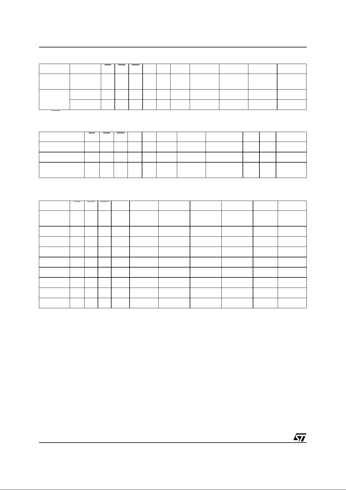
Table 7. Program, Erase Times and Program/Erase Endurance Cycles
Parameter Test Conditions
Word Program
Double Word Program
Main Block Program
Parameter Block Program
Main Block Erase
Parameter Block Erase
Program/Erase Cycles (per Block) 100,000 cycles
V
PPF=VDDF
V
= 12V ±5%
PPF
= 12V ±5%
V
PPF
V
PPF=VDDF
V
= 12V ±5%
PPF
V
PPF=VDDF
= 12V ±5%
V
PPF
V
PPF=VDDF
V
= 12V ±5%
PPF
V
PPF=VDDF
Flash Memory
Unit
Min Typ Max
10 200 µs
10 200 µs
0.16 5 s
0.32 5 s
0.02 4 s
0.04 4 s
110 s
110 s
0.8 10 s
0.8 10 s
Flash Block Locking
The Flash Memory features an instant, individual
block locking scheme that allows any block to be
lockedorunlockedwithnolatency.Thislocking
scheme has three levels of protection.
■ Lock/Unlock - this first level allows softwa r e-
only control of block locking.
■ Lock-Down - this second level requires
hardware interaction before locking can be
changed.
■ V
PPF
≤ V
- the third level offers a comp let e
PPLK
hardware protection againstprogram and erase
on all blocks.
The locking status of each block can be set to
Locked, Unlocked, and Lock-Down. The following
sections explain t he operation of the locking system. Table 7, defines all of the poss ible loc king
states (WP
, DQ1, DQ0), and Appendix C, Figure
30, shows a flowchart for the locking operations.
Locked State. The default status of all blocks on
power-up or reset is Locked (states (0,0,1) or
(1,0,1)). L oc ked blocks are fully protected from
any prog ram or erase. Any program or erase operations attempted on a locked block will return an
error in the Status Register. The Status of a
Locked block can be chang ed to Unlocked or
Lock-Down using the appropriate software commands.An Unlockedblockcan beLockedby issuing the Lock command.
Unlocked State. Unlocked blocks (states (0,0,0),
(1,0,0) (1,1,0)), can be programmed or erased. All
unlocked blocks return to the Locked state when
the device is reset or powered-dow n. The status of
an unlocked bloc k can be changed to Locked or
Locked-Down using the appropriate s oftware
commands. A locked block can be unlocked by issuing the Unlock command.
Lock-Down State. Blocks that are Locked-Down
(state (0,1,1))are protected from program and
erase operations (as for Locked blocks) but their
Lock status cannot be changed using software
commands alone. A Lockedor U nlock ed block can
be Locked-Down by issuing the Lock-Down command. Locked-Down bloc ks revert to the Locked
state when the device is reset or powered-down.
The Lock- Down function is dependent on the WPF
input pin. When WPF=0 (VIL), the blocks in the
Lock-Down state (0, 1,1) are protected from program, erase and lock status changes. When
=1 (VIH) the Lock- Down f unc t ion is disabled
WPF
(1,1,1) and Locked-Down blocks can be individually unlocked to t he (1,1,0) state by issuing the
software command , wherethey canbe erased and
programmed. These blocks can then be re-locked
(1,1,1) and unlocked (1,1,0) as desired while WPF
remains high. When WPF is low, blocks that were
previously Locked-Down return to the Lock-Down
state (0, 1,1) regardless of any changes made
while WPF
was high. Device reset or pow er-down
resets all blocks, includingthose in Lock-Down, to
the Locked state.
17/57
M36W432T, M36W432B
Reading a Block’s Lock Status. The lock status
of every block can be read in the R ead Electronic
Signature mode of the device. To enter this mode
write90h tothe device. Subsequent reads atBlock
Address 00002h wil l output the lo ck status of that
block. The lock status is represented by DQ0 and
DQ1. DQ0 indicates the Block Lock/Unlock status
and is set by the Lock command and cleared by
the Unlock command. it is also automatically set
when entering Loc k -Down. DQ1 indicates the
Lock-Down status and is s et by the Lock-Down
command. It c annot b e cleared by software, only
by a device reset or power-down.
Locking Operations During Erase Suspend.
Changes to block lock status c an be performed
during an erase suspend by using the standard
locking command sequences to unlock, lock or
lock-down a block. This is useful in the case when
To change block locking d uring an erase operation, first write the Erase Suspend command, then
check the status register un til it indicates that the
erase operation has been suspended. Next write
the desired Lock command sequenc e to a block
and the lockstatus will be changed. After com pleting any desired lock, read, or program operations,
resume the erase operation w ith the Eras e Resume command.
If a blockis locked or locked-down during an erase
suspend of the same block, the locking status bits
will be changed immediately, but when the erase
is resumed, the erase operation will complete.
Locking operations cannot be performed during a
program suspend. Refer to Appendix D, Command Interface and Program/E ras e Controller
State, for detailed inform ation on which commands are valid during erase suspend.
another block needs to be updated whi le an erase
operation is in progress.
Table 8. Block Lock Status
Item Address Data
Block Lock Configuration xx002 LOCK
Block is Unlocked DQ0=0
Block is Locked DQ0=1
Block is Locked-Down DQ1=1
Table 9. Lock Status
Current
Lock Status
(WPF,DQ1,DQ0)
Current State
1,0,0 yes 1,0,1 1,0,0 1,1,1 0,0,0
(2)
1,0,1
1,1,0 yes 1,1,1 1,1,0 1,1,1 0,1,1
1,1,1 no 1,1,1 1,1,0 1,1,1 0,1,1
0,0,0 yes 0,0,1 0,0,0 0,1,1 1,0,0
(2)
0,0,1
0,1,1 no 0,1,1 0,1,1 0,1,1
Note: 1. The lock status is defined by the write protect pin and by DQ1 (‘1’ for a locked-down block) and DQ0 (‘1’ for a locked block) as read
in the Read Electronic Signature command with A1 = V
2. All blocks are locked at power-up, so the default configuration is 001 or 101 according to WPF
3. A WPF
transition to VIHon a locked block will restore the previous DQ0 value, giving a 111 or 110.
(1)
Program/Erase
Allowed
no 1,0,1 1,0,0 1,1,1 0,0,1
no 0,0,1 0,0,0 0,1,1 1,0,1
After
Block Lock
Command
andA0=VIL.
IH
Next Lock Status
(WPF, DQ1, DQ0)
After
Block Unlock
Command
(1)
After Block
Lock-Down
Command
status.
After
transition
WPF
1,1,1 or 1,1,0
(3)
18/57

M36W432T, M36W432B
Flash Status Register
The Status Register provides information on the
current or previous Program or Erase operation.
The various bits convey information and errors on
the operation. To read the Status register the
Read Status Register command can be issued,refer to Read Status Register Command section. To
output the contents, t he Status Register is lat c hed
on the falling edge of the Chip Enable or Output
Enable signals, and can be read until Chip E nable
or Output Enable returns to V
. Either Chip En-
IH
able or Output Enable must be toggled to update
the latched data.
Bus R ead op erati ons from any address always
read the Status Register during Program and
Erase operations.
The bits in the Status Register are summarized in
Table 10, Status Register Bits. R efer to Table 10
in conjunction with the following text descriptions.
Program/Erase Controller Status (Bit 7). The Program/Erase ControllerStatus bit indicates whether
the Program/Erase Controller is active or inac tive.
When the Program /Erase Controller Status bit is
Low (set to ‘0’), the Program/Erase Controller is
active; when the bit is High (set to ‘1’), the Program/Erase Controller is inactive, and the device
is ready to process a new command.
The Program/Erase Controller Status is Low immediately after a Program/Erase Suspen d command is issued un til the Program/Erase Controller
pauses. After the Program/Erase Controller pauses the bit is High.
During Program, Erase, operat ions t he Program/
EraseControllerStatusbitcanbepolledtofindthe
end of the operation. Other bits in the Stat us Register should not be tested until the Program/Erase
Controller completes the operation and the bit is
High.
After the Program/Erase Controll er c ompletes its
operation the Eras e Status, Program Status, V
PPF
Status and Block Lock Status bits shouldbe tested
for errors.
Erase Suspend Status (Bit 6). T he Erase Suspend St atu s bit indicates that an Erase operation
has been suspended or is going to be suspended.
When the Erase Suspend Status bit is High (set to
‘1’), a Program/Eras e Suspend c ommand has
been issued and the memory is waiting for a Program/Erase Resume command.
The Erase Sus pend Status should only be considered valid when the Program/Erase ControllerStatus bit is High (Program/Erase Controller inactive).
Bit 7 is set within 30µ s of the Program/Erase Sus-
pend command being issued therefore the memory may still complete the operation rather than
entering the Suspend mode.
When a Program/Erase Resume command is issued the Erase Suspend Status bit returns Low.
Erase Status (Bit 5). The Erase Status bit canbe
used to identify if the memory has failed to verify
that the block has eras ed correctly. When the
Erase Stat us bit is High (set to ‘1’), the P rogram/
Erase Controller has applied the maximum number of pulses to the block and s ti ll failed to verify
thatthe blockhas erased correctly.The Eras e Status bit s hould be read once the Program/Erase
Controller Status bit is High (Program/Erase Controller inactive).
Once setHigh, t he Erase St atus bit can only be reset Low by a Clear Status Register command or a
hardware reset. If set High it should be reset before a new Program or Erase command is issued,
otherwise the new command will appear to fail.
Program Status (Bit 4). The Program Statu s bit
is used to identify a Program failure. When the
Program Status bi t is High (set to ‘1’), the Program/Erase Controller h as applied the maximum
number of pulses to the byte and still failed to verify that it has programm ed c orrectly. The Program
Status bitshould be read once the Program/Erase
Controller Status bit is High (Program/Erase Controller inactive).
Once set High, the Program Status bit can only be
reset Low by a Clear Status Register command or
a hardware res et. If set High it should be reset before a new command is issued, otherwise the new
command will appear to fail.
Status (Bit 3). The V
V
PPF
used to identify an invalid voltage on the V
during Program and Erase operations . The V
Status bit can be
PPF
PPF
pin
PPF
pin is only sampled at the beginning of a Program
or Erase operation. Indeterminate r es ult s can occur if V
When the V
voltageontheV
voltage; when the V
‘1’), the V
V
PPF
becomes invalid during an operation.
PPF
Status bit is Low (set to ‘0’), the
PPF
pin has a voltage that is below t he
PPF
Lockout Voltage, V
pin was sam pled at a v alid
PPF
Status bit is High (set to
PPF
, the memory is pro-
PPLK
tected and Program and Erase operations cannot
be performed.
Once set High, the V
Status bitcanonly be re-
PPF
set Low by a Clear Status Register command or a
hardware reset. If set High it should be reset before a new Program or Erase command is issued,
otherwise the new command will appear to fail.
19/57
M36W432T, M36W432B
Program Suspend Status (Bit 2). The Program
Suspend Status bit indicates that aProgram operation has been suspended. When the Program
Suspend Status bit is High (set to ‘1’), a Program/
Erase Suspend command has been issued and
the memory is waitin g f or a Program/Erase Resume command. The Program Suspend Status
should only be considere d valid when the Program/Erase Controller Status bit is High (Program/
Erase Controller inactive). Bit 2 is set within 5µs of
the Program/Erase Suspend command being issued therefore the memory may still complete t he
operation rather than entering the Suspend mode.
When a Program/Erase Resume command is issued the Program Suspend Statusbit returns Low.
Block Protection Status (Bit 1). The Block ProtectionStatusbitcanbeusedtoidentifyifaProgram or Erase operation has tried to m odify the
contents of a locked block.
When the Block Protection Status bit is High (set
to ‘1’), a Program or Erase operation has been attemptedonalockedblock.
Once set High, the Block Protection Status bit can
only be reset Low by a Clear Sta tus Register command or a hardware reset. If set High it should be
reset before a new command is issued, otherwise
the new command will appear to fail.
Reserved (Bit 0). Bit 0 of the Status Register is
reserved. Its value must be masked.
Note: Refer to Appendix C, Flowcharts and
Pseudo Codes, for using the Status Register.
Table 10. Status Register Bits
Bit Name Logic Level Definition
7 P/E.C. Status
6 Erase Suspend Status
5 Erase Status
'1' Ready
'0' Busy
'1' Suspended
'0' In progress or Completed
'1' Erase Error
'0' Erase Success
4 Program Status
V
3
2 Program Suspend Status
1 Block Protection Status
0 Reserved
Note: Logic level '1' is High, '0' is Low.
PPF
Status
SRAM Operations
There arefive standard operations th at control the
SRAM component. These are Bus Read, Bus
Write, Standby/Power-down, Data Retention and
Output Disable. A summary is shown in Table 2,
Main Operation Modes
Read. Read operations are used to output the
contents of theSRAM Array. TheSRAM i s inRead
mode whenever Write Enable, WS
put Enable, GS
,isatVIL, Chip Enable, E1S,isat
,isatVIH,Out-
'1' Program Error
'0' Program Success
V
'1'
'0'
'1' Suspended
'0' In Progress or Completed
'1' Program/Erase on protected block, Abort
'0' No operation to protected blocks
V
, Chip Enable,E2S, isatVIH, and ByteEnables,
IL
and LBS are at VIL.
UBS
Invalid, Abort
PPF
V
OK
PPF
Valid data will be available onthe output pins after
atimeoft
after the last stable address. If the
AVQV
Chip Enable or Output Enable access t imes are
not met, data access will be measured from the
limiting parameter (t
E1LQV,tE2HQV
,ort
GLQV
) rather than the address. Data out may be indeterminate at t
E1LQX,tE2HQX
will always be valid at t
and t
AVQV
, but data lines
GLQX
(see Table 19,Figures
13 and 14).
20/57
M36W432T, M36W432B
Write. Write operations are used t o write data to
the SRAM. The SRAM is in Write mode whenever
and E1S are at VIL,andE2SisatVIH. Either
WS
the Chip Enable inputs, E1S
Enable input, WS
, must be deas serted during ad-
and E 2S, or the Write
dress transitions for subsequent write cycles.
A Write operation is initiated when E1S
E2S is at V
on the falling edge of E1S
or the falling edge of WS
and WS is atVIL. The data is latched
IH
, the rising edge of E2S
, whichever occurs last.
is at VIL,
The Write cycle is terminatedon therising ed ge of
, the rising edge of WS or the f alling e dge of
E1S
E2S, whichever occurs first.
If the O utpu t is enabled (E1S
=VIL), then WS wil l return the outputs to high
GS
impedance wit hin t
WLQZ
=VIL,E2S=VIHand
of its falling edge. Care
must be taken to avoid bus contention in this type
of operation. The Data input must be valid for t
before the rising edge of Write Enable, for
VWH
t
before the rising edge of E1S or for t
DVE1H
D-
DVE2L
before the falling edge of E2S, whichever occurs
MAXIMUM RATING
Stressingthedeviceabovetheratinglistedinthe
Absolute Maximum Ratings table may cause permanent damage to the device. These are stress
ratings only and operation of the device at these or
any other conditions above those indicated i n the
Operating sections of this specification is no t im-
first, and remain valid for t
WHDX,tE1HAX
or t
E2LAX
(see Table 20, Figure 16, 17, 18 and 19).
Standby/Power-Down . The SRAM component
has a chip enabled power-down feature wh ich invokes an automatic st andby mode (see Table 19,
Figure 15). The SRAM is in Standby mode whenever either Chip Enable is deasserted, E1S
at V
IH
or E2S at VIL.
Data Retention. The SRAM data retention per-
formances as V
goes d own to VDRare de-
DDS
scribedinTable21andFigure20,21.InE1S
controlled data retention mode, the minimum
standby current mode is entered w hen
E1S
≥ V
E2S ≥ V
– 0.2V and E 2S ≤ 0.2V or
DDS
– 0.2V. In E2S controlled data reten-
DDS
tion mode, minimum standby current mode is entered when E2S ≤ 0.2V.
Output Disable. The data ou tpu ts are high im pedance when the Output Enable, GS
,isatV
IH
with Write Enable, WS,atVIH.
plied. E x posure to Absolute Maximum Rating conditions for extended periods may affect device
reliability. Refer also to the STMicroele ctronics
SURE Program and other relevan t quality documents.
Table 11. Absolute Maximum Ratings
Symbol Parameter
T
A
T
BIAS
T
STG
V
IO
V
DDF,VDDQF
V
PPF
V
DDS
Note: 1. Depends on range.
Ambient Operating Temperature
Temperature Under Bias –40 125 °C
Storage Temperature –55 155 °C
Input or Output Voltage –0.5
Flash Supply Voltage –0.6 3.9 V
Program Voltage –0.6 13 V
SRAM Supply Voltage –0.5 3.9 V
(1)
Value
Min Max
–40 85 °C
V
+0.3
DDQF
Unit
V
21/57

M36W432T, M36W432B
DC AND AC PARAMETERS
This section summarizes the operating and m easurement conditions, and the DC and AC c harac teristics of the device. The parameters in the DC
and AC characteristics Tables that follow, are derived from tests performed under the M eas ure-
Table 12. Operating and AC Measurement Conditions
ment Conditions s ummarized in Table 12,
Operating and AC Measurem ent Conditions. Designers should check that the operat ing conditions
in their circuit match the measurement conditions
when relying on the quoted parameters.
SRAM Flash Memory
Parameter
Min Max Min Max
Supply Voltage
V
DDF
V
DDQ F =VDDS
Supply Voltage
– – 2.7 3.3 V
2.7 3.3 2.7 3.3 V
Ambient Operating Temperature – 40 85 – 40 85 °C
Load Capacitance (C
)
L
50 50 pF
Input Rise and Fall Times 5 5 ns
Input Pulse Voltages
Input and Output Timing Ref. Voltages
Figure 7. AC Measurement I/O Waveform
V
DDQ
V
0V
AI05205
Note: V
DDQ
means V
DDQF=VDDS
DDQ
0toV
DDQF
V
/2 V
DDQF
Figure 8. AC Measurement Load Circuit
/2
V
DDQF
V
DDF
0toV
DDQF
DEVICE
UNDER
TEST
DDQF
/2
V
DDQF
25kΩ
Units70 70/85
V
V
0.1µF
0.1µF
CL includes JIG capacitance
CL
Table 13. Device Capacitance
Symbol Parameter Test Condition Typ Max Unit
V
C
IN
C
OUT
Note: Sampled only, not 100% tested.
Input Capacitance
Output Capacitance
22/57
=0V,f=1MHz
IN
V
=0V,f=1MHz
OUT
12 14 pF
20 22 pF
25kΩ
AI05206

M36W432T, M36W432B
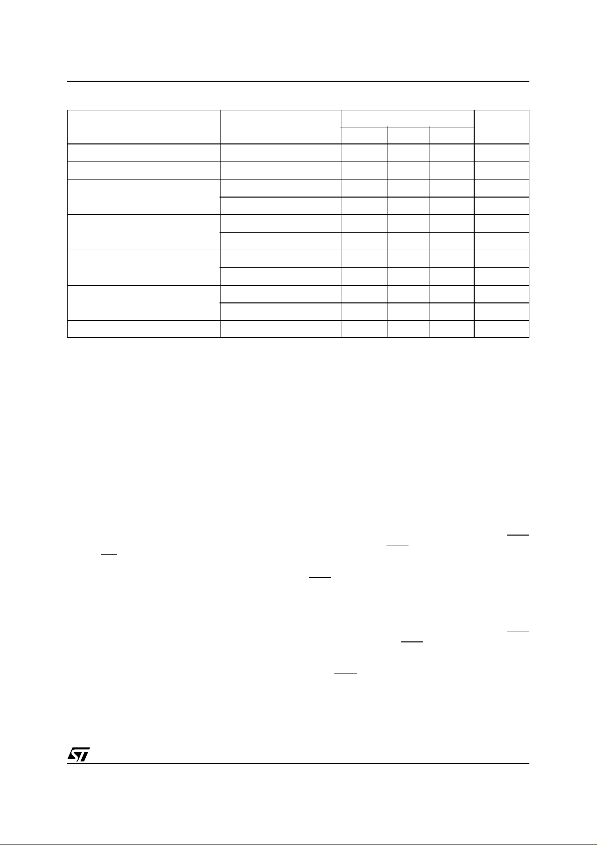
Table 14. DC Characteristics
Symbol Parameter Device Test Condition Min Typ Max Unit
I
LI
I
LO
I
DDSVDD
I
DDD
I
DD
I
DDR
I
DDW
I
DDE
I
DDES
I
DDWS
Input Leakage Current
Output Leakage Current
Flash &
SRAM
Flash &
SRAM
Flash
Standby Current
SRAM
Supply Current (Reset) Flash
0V ≤ V
0V ≤ V
SRAM Outputs Hi-Z
EF
V
DDQF=VDDF
E1S
=E2S≥ V
RPF
V
IN
≤ V
IN
DDQF
≤ V
OUT
DDQF,
=V
DDQF
± 0.2V
DDS
or E2S ≤ 0.2V
=V
± 0.2V
SSF
≤ V
– 0.2V
DDS
≤ 0.2V
or V
IN
max
–0.2V
±2 µA
±10 µA
15 50 µA
20 50 µA
15 50 µA
12mA
IIO= 0 mA, cycle time = 1µs
Supply Current SRAM
≤ V
DDS
– 0.2V
f=5MHz
IH,
712mA
10 20 mA
Supply Current (Read) Flash
Supply Current (Program)
Flash Program in progress 10 20 mA
V
IN
or VIN≤ 0.2V
I
= 0 mA, min cycle time
IO
EF
=VIL,GF=V
Supply Current (Erase) Flash Erase in progress 5 20 mA
Supply Current
(Erase Suspend)
Supply Current
(Program Suspend)
Flash Erase Suspend in progress 50 µA
Flash
Program Suspend in progress
50 µA
I
PPS
I
PPR
I
PPW
I
PPE
V
IL
V
IH
V
OL
V
OH
V
PPL
Program Current
(Standby)
Program Current
(Read)
Program Current
(Program)
Program Current
(Erase)
Input Low Voltage
Input High Voltage
Output Low Voltage
Output High Voltage
Program Voltage (Program or
Erase operations)
Flash
Flash
Flash
Flash
Flash &
SRAM
Flash &
SRAM
Flash &
SRAM
Flash &
SRAM
≤ V
PPF
DDQF
> V
V
PPF
DDF
V
≤ V
PPF
DDQF
V
PPF=VDDF
= 12V ± 0.6V
V
PPF
Program in progress
= 12V ± 0.6V
V
PPF
Program in progress
V
DDQF=VDDS
V
DDQF=VDDS
V
DDQF=VDDS=VDD
V
DDQF=VDDS=VDD
I
OL
= 100µA
IOH= –100µA
≥ 2.7V
≥ 2.7V
min
min
– 0.3 0.8 V
2.2
V
DDQ
–0.1
0.2 5 µA
100 400 µA
0.2 5 µA
100 400 µA
510mA
510mA
V
DDQF
+0.3
0.1 V
V
Flash 2.7 3.3 V
V
V
23/57

M36W432T, M36W432B
Symbol Parameter Device Test Condition Min Typ Max Unit
V
V
V
Figure 9. Flash Read AC Waveforms
Program Voltage
PPH
(Program or Erase operations)
Program Voltage
PPLK
(Program and Erase lock-out)
V
Supply Voltage (Program
LKO
DDF
and Erase lock-out)
Flash 11.4 12.6 V
Flash 1 V
Flash 2 V
tAVAV
A0-A20
tAVQV
EF
tELQV
tELQX
GF
tGLQX
DQ0-DQ15
ADDR. VALID
CHIP ENABLE
OUTPUTS
ENABLED
Table 15. Flash Read AC Characteristics
Symbol Alt Parameter
(1)
(1)
(1)
t
Address Valid to Next Address Valid Min 70 85 ns
RC
t
Address Valid to Output Valid Max 70 85 ns
ACC
t
Address Transition to Output Transition Min 0 0 ns
OH
t
Chip Enable High to Output Transition Min 0 0 ns
OH
t
Chip Enable High to Output Hi-Z Max 20 20 ns
HZ
t
Chip Enable Low to Output Valid Max 70 85 ns
CE
t
Chip Enable Low to Output Transition Min 0 0 ns
LZ
t
Output Enable High to Output Transition Min 0 0 ns
OH
t
Output Enable High to Output Hi-Z Max 20 20 ns
DF
t
Output Enable Low to Output Valid Max 20 20 ns
OE
t
AVAV
t
AVQV
t
AXQX
t
EHQX
t
EHQZ
t
ELQV
t
ELQX
t
GHQX
t
GHQZ
t
GLQV
(1)
(1)
(2)
(1)
(2)
tGLQV
VALID
tAXQX
tEHQX
tEHQZ
tGHQX
tGHQZ
VALID
DATA VALID STANDBY
AI05207
Flash
Unit
70 85
24/57

M36W432T, M36W432B
Symbol Alt Parameter
(1)
t
t
GLQX
Note: 1. Sampled only, not 100% tested.
maybe delayed by up to t
2. GF
Output Enable Low to Output Transition Min 0 0 ns
OLZ
ELQV-tGLQV
after the falling edge of EF without increasing t
Flash
70 85
.
ELQV
Unit
25/57
M36W432T, M36W432B
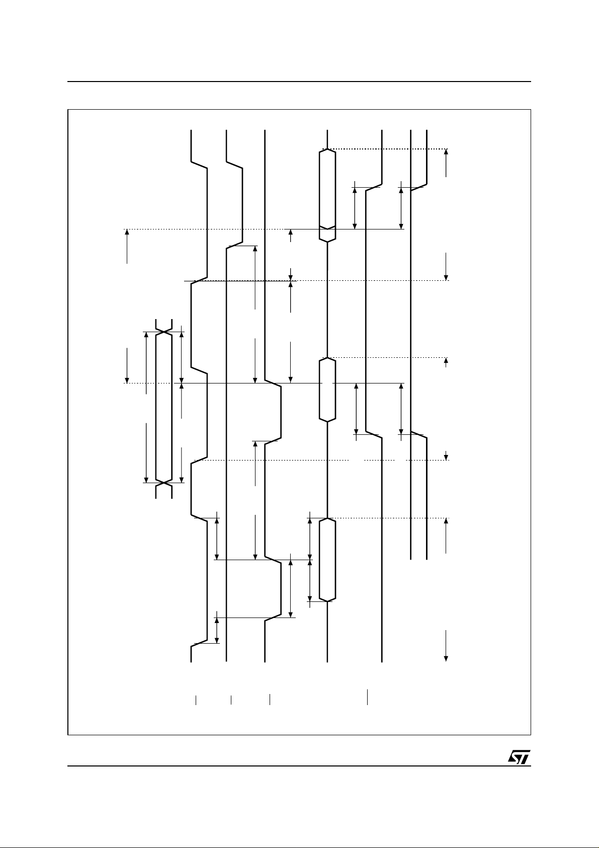
Figure 10. Flash Write AC Waveform s, Write Enable Controlled
AI05208
tWHAX
PROGRAM OR ERASE
tAVAV
VALIDA0-A20
tAVWH
tWHGL
tELQV
tWHEL
tQVWPL
STATUS REGISTER
tQVVPL
READ
1st POLLING
STATUS REGISTER
OR DATA INPUT
26/57
EF
tELWL tWHEH
GF
tWHWL
WF
tWLWH
tWHDXtDVWH
DQ0-DQ15 COMMAND CMD or DATA
tWPHWH
WPF
tVPHWH
PPF
V
SET-UP COMMAND CONFIRM COMMAND
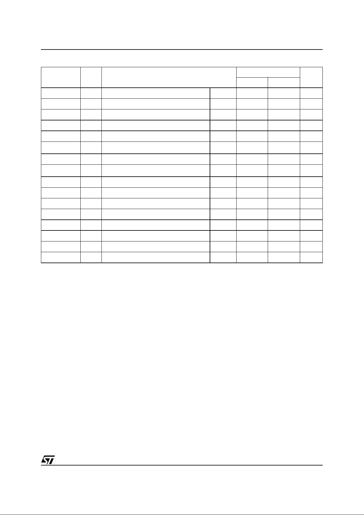
Table 16. Flash Write AC Characteristics, Write Enable Controlled
Symbol Alt Parameter
t
AVAV
t
AVWH
t
DVWH
t
ELWL
t
ELQV
(1,2)
t
QVVPL
t
QVWPL
t
Note: 1. Sampled only, not 100% tested.
(1)
VPHWH
t
WHAX
t
WHDX
t
WHEH
t
WHEL
t
WHGL
t
WHWL
t
WLWH
t
WPHWH
2. Applicable if V
t
Write Cycle Time Min 70 85 ns
WC
t
Address Valid to Write Enable High Min 45 45 ns
AS
t
Data Valid to Write Enable High Min 45 45 ns
DS
t
Chip Enable Low to Write Enable Low Min 0 0 ns
CS
Chip Enable Low to Output Valid Min 70 85 ns
Output Valid to V
PPF
Low
Min 0 0 ns
Output Valid to Write Protect Low Min 0 0 ns
t
VPSVPPF
t
AH
t
DH
t
CH
High to Write Enable High
Min 200 200 ns
Write Enable High to Address Transition Min 0 0 ns
Write Enable High to Data Transition Min 0 0 ns
Write Enable High to Chip Enable High Min 0 0 ns
Write Enable High to Output Enable Low Min 25 25 ns
Write Enable High to Output Enable Low Min 20 20 ns
t
Write Enable High to Write Enable Low Min 25 25 ns
WPH
t
Write Enable Low to Write Enable High Min 45 45 ns
WP
Write Protect High to Write Enable High Min 45 45 ns
is seen as a logic input (V
PPF
PPF
<3.6V).
M36W432T, M36W432B
Flash
Unit
70 85
27/57

M36W432T, M36W432B
Figure 11. Flash Write AC Waveforms, Chip Enable Controlled
AI05209
tEHAX
PROGRAM OR ERASE
tAVAV
VALIDA0-A20
tAVEH
tEHGL
tELQV
tQVWPL
CMD or DATA STATUS REGISTER
tQVVPL
READ
1st POLLING
STATUS REGISTER
OR DATA INPUT
CONFIRM COMMAND
28/57
WF
tWLEL tEHWH
GF
tEHEL
EF
tELEH
tEHDX
tDVEH
tWPHEH
DQ0-DQ15 COMMAND
WPF
tVPHEH
PPF
V
POWER-UP AND
SET-UP COMMAND
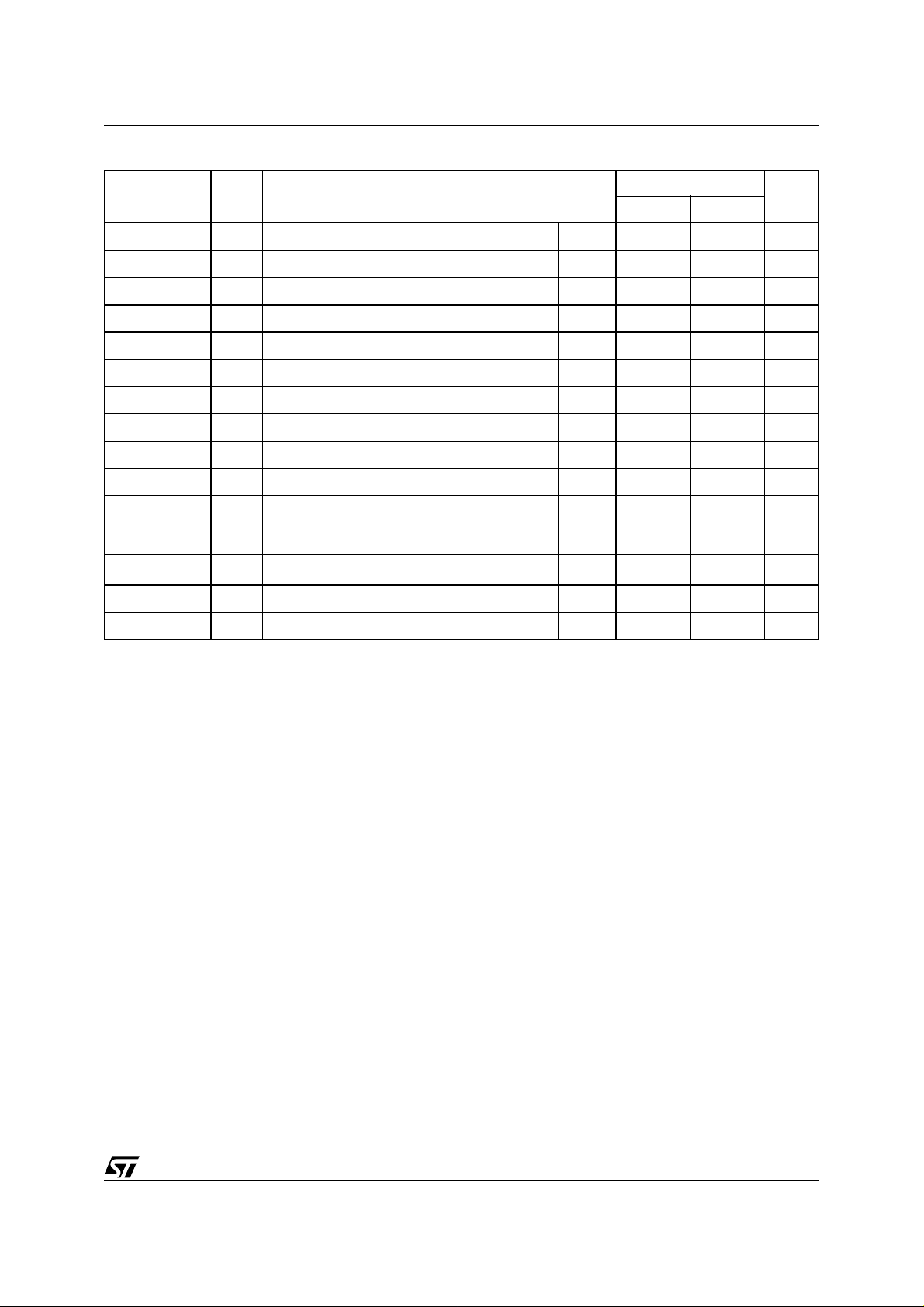
Table 17. Flash Write AC Characteristics, Chip Enable Controlled
Symbol Alt Parameter
t
AVAV
t
AVEH
t
DVEH
t
EHAX
t
EHDX
t
EHEL
t
EHGL
t
EHWH
t
ELEH
t
ELQV
(1,2)
t
QVVPL
t
QVWPL
(1)
t
VPHEH
t
WLEL
t
WPHEH
Note: 1. Sampled only, not 100% tested.
2. Applicable if V
t
Write Cycle Time Min 70 85 ns
WC
t
Address Valid to Chip Enable High Min 45 45 ns
AS
t
Data Valid to Chip Enable High Min 45 45 ns
DS
t
Chip Enable High to Address Transition Min 0 0 ns
AH
t
Chip Enable High to Data Transition Min 0 0 ns
DH
t
Chip Enable High to Chip Enable Low Min 25 25 ns
CPH
Chip Enable High to Output Enable Low Min 25 25 ns
t
Chip Enable High to Write Enable High Min 0 0 ns
WH
t
Chip Enable Low to Chip Enable High Min 45 45 ns
CP
Chip Enable Low to Output Valid Min 70 85 ns
Output Valid to V
PPF
Low
Data Valid to Write Protect Low Min 0 0 ns
t
VPSVPPF
t
CS
High to Chip Enable High
Write Enable Low to Chip Enable Low Min 0 0 ns
Write Protect High to Chip Enable High Min 45 45 ns
is seen as a logic input (V
PPF
PPF
<3.6V).
M36W432T, M36W432B
Flash
Unit
70 85
Min 0 0 ns
Min 200 200 ns
29/57

M36W432T, M36W432B
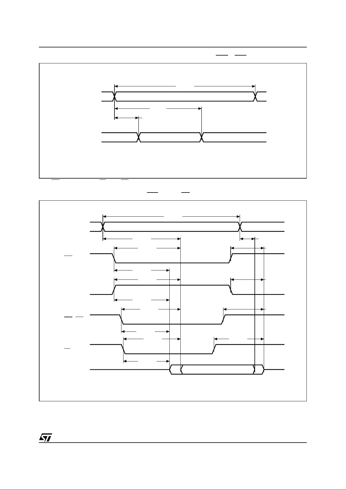
Figure 12. Flash Power-Up and Reset AC Waveforms
EF,GF
WF,
RPF
tPHWL
tPHEL
tPHGL
tPHWL
tPHEL
tPHGL
tVDHPH
VDDF, VDDQF
Power-Up Reset
Table 18. Flash Power-Up and Reset AC Characteristics
Symbol Parameter Test Condition
t
PHWL
t
PHEL
t
PHGL
t
PLPH
t
VDHPH
Note: 1. The device Reset is possible but not guaranteed if t
2. Sampled only, not 100% tested.
3. It is important to assert RPF
Reset High to Write Enable Low,Chip Enable
Low, Output Enable Low
(1,2)
Reset Low to Reset High Min 100 100 ns
(3)
Supply Voltages High to Reset High Min 50 50 µs
in order to allow proper CPU initialization during power up or reset.
PLPH
< 100ns.
During
Program and
Erase
others Min 30 30 ns
tPLPH
AI05210
Flash
Unit
70 85
Min 50 50 µs
30/57
M36W432T, M36W432B
Figure 13. SRAM Read AC Waveforms, Address Controlled with UBS =LBS=V
tAVAV
A0-A17
tAVQV
tAXQX
DQ0-DQ15
Note: E1S = Low, E2S = High,GS =Low,WS= High.
VALID
DATA VALIDDATA VALID
AI05211
Figure 14. SRAM Read AC Waveforms, E1S,E2SorGSControlled
tAVAV
A0-A17
VALID
IL
E1S
E2S
UBS, LBS
GS
DQ0-DQ15
tAVQV tAXQX
tE1LQV
tE1LQX
tE2HQV
tE2HQX
tBLQV
tBLQX
tGLQV
tGLQX
DATA VALID
tGHQZ
tE1HQZ
tE2LQZ
tBHQZ
AI05212
31/57
M36W432T, M36W432B
Figure 15. SRAM Standby AC Waveforms
E1S
E2S
I
DD
tPU
50%
Table 19. SRAM Read AC Characteristics
Symbol Alt Parameter
t
AVAV
t
AVQV
t
AXQX
t
BHQZ
t
BLQV
t
BLQX
t
E1HQZ
t
E1LQV
t
E1LQX
t
E2HQV
t
E2HQX
t
E2LQZ
t
GHQZ
t
GLQV
t
GLQX
(1)
t
PD
(1)
t
PU
Note: 1. Sampled only. Not 100% tested.
t
t
t
t
BHZ
t
t
t
HZ1
t
CO1
t
t
CO2
t
t
HZ2
t
OHZ
t
t
OLZ
RC
AA
OH
BA
BLZ
LZ1
LZ2
OE
Read Cycle Time 70 ns
Address Valid to Output Valid 70 ns
Address Transition to Output Transition 10 ns
UBS, LBS Disable to Hi-Z Output 25 ns
UBS, LBS Access Time 70 ns
UBS, LBS Enable to Low-Z Output 10 ns
Chip Enable 1 High to Output Hi-Z 25 ns
Chip Enable 1 Low to Output Valid 70 ns
Chip Enable 1 Low to Output Transition 10 ns
Chip Enable 2 High to Output Valid 70 ns
Chip Enable 2 High to Output Transition 10 ns
Chip Enable 2 Low to Output Hi-Z 25 ns
Output Enable High to Output Hi-Z 25 ns
Output Enable Low to Output Valid 35 ns
Output Enable Low to Output Transition 5 ns
Chip Enable 1 High or Chip Enable 2 Low to Power Down 70 ns
Chip Enable 1 Low or Chip Enable 2 High to Power Up 0 ns
tPD
AI05213
SRAM
Unit
Min Max
32/57
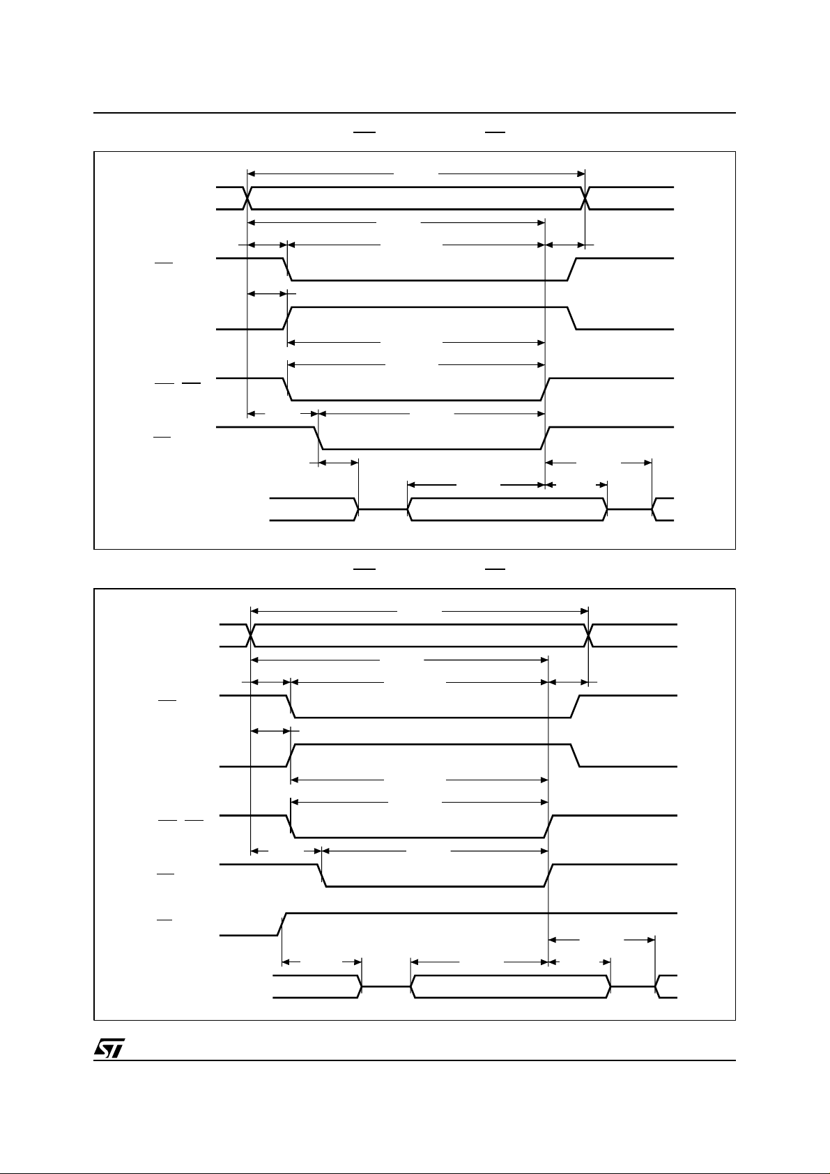
Figure 16. SRAM Write AC Waveforms, WS Controlled with GS Low
tAVAV
M36W432T, M36W432B
A0-A17
tAVE1L
E1S
tAVE2H
E2S
UBS, LBS
WS
tWLQZ
DQ0-DQ15
Figure 17. SRAM Write AC Waveforms, WS
VALID
tAVWH
tE1LWH
tE2HWH
tBLWH
tWLWHtAVWL
tDVWH
INPUT VALID
Controlled with GS High
tWHAX
tWHQX
tWHDX
AI05214
A0-A17
E1S
E2S
UBS, LBS
WS
GS
DQ0-DQ15
tAVE1L
tAVE2H
tGHQZ
tAVAV
VALID
tAVWH
tE1LWH
tE2HWH
tBLWH
tWHAX
tWLWHtAVWL
tWHQX
tDVWH
INPUT VALID
tWHDX
AI05215
33/57
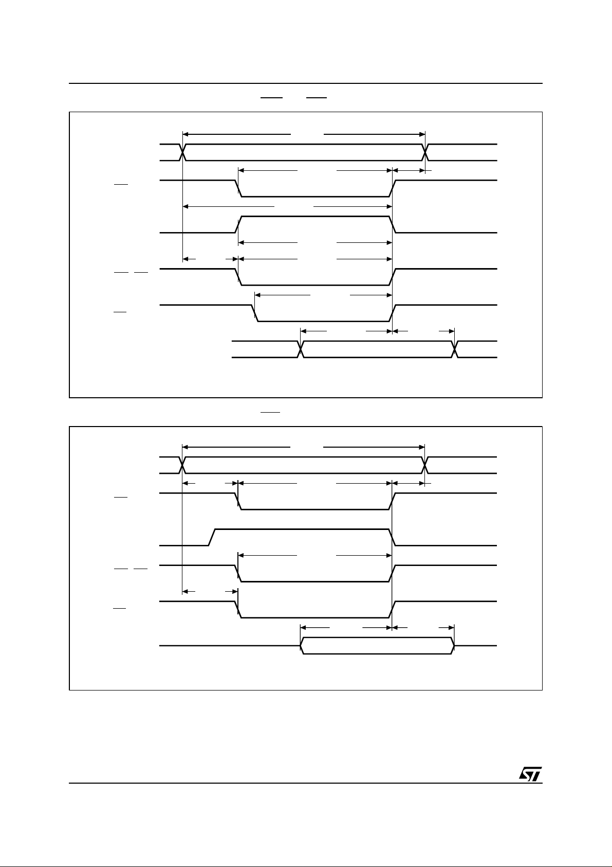
M36W432T, M36W432B
Figure 18. SRAM Write AC Waveforms, UBS and LBS Controlled
tAVAV
A0-A17
E1S
E2S
tAVWL
UBS, LBS
WS
DQ0-DQ15
Figure 19. SRAM Write AC Waveforms, E1S
VALID
tE1LWH
tAVWH
tE2HWH
tBLWH
tWLWH
Controlled
tAVAV
tDVWH
tE1HAX
tWHDX
DATA VALID
AI05216
A0-A17
E1S
E2S
UBS, LBS
WS
DQ0-DQ15
tAVE1L
tAVWL
VALID
tE1LWH
tBLWH
tDVE1H
tE1HAX
tWHDX
INPUT VALID
AI05217
34/57
Table 20. SRAM Write AC Characteristics
Symbol Alt Parameter
t
AVAV
t
AVE1L
t
AVE2H
t
AVWH
t
AVWL t
t
BLWH
t
DVE1H
t
DVE2L
t
DVWH
t
E1HAX
,
t
E1LWH
t
E2HWH
t
E2LAX
t
GHQZ
t
WHAX t
t
WHDX
t
WHQX
t
WLQZ
t
WLWH t
Note: 1. tASis measured from the address valid to the beginning of write.
2. t
WR
3. t
CW
4. A Write occurs during the overlap (t
UBS
liest transition whenE1S
t
WC
t
AS
t
AS
t
AW
AS
t
BW
t
DW
t
DW
t
DW
t
WR
t
CW
t
WR
t
GHZ
WR
t
t
OW
t
WHZ
WP
is measured from the end or write to the address change. tWRappliedincaseawriteendsasE1Sor WS going high.
is measured from E1S going low end of write.
or LBS forsingle byteoperationor simultaneouslyasserting UBSandLBSfor double byte operation. A write ends at the ear-
Write Cycle Time 70 ns
(1)
Address Valid to Chip Enable 1 Low 0 ns
(1)
Address Valid to Chip Enable 2 High 0 ns
Address Valid to Write Enable High 60 ns
(1)
Address Valid to Write Enable Low 0 ns
UBS, LBS Valid to End of Write 60 ns
Input Valid to Chip Enable 1 High 30 ns
Input Valid to Chip Enable 2 Low 30 ns
Input Valid to Write Enable High 30 ns
(2)
Chip Enable 1 High to Address Transition 0 ns
(3)
Chip Select to End of Write 60 ns
(2)
Chip Enable 2 Low to Address Transition 0 ns
Output Enable High to Output Hi-Z 25 ns
(2)
Write Enable High to Address Transition 0 ns
Write Enable High to Input Transition 0 ns
DH
Write Enable High to Output Transition 10 ns
Write Enable Low to Output Hi-Z 25 ns
(4)
Write Enable Pulse Width 50 ns
)oflowE1Sandlow WS.A write begins when E1S goes low and WS goes low withasserting
WP
goes high and WS goes high. The tWPis measured from the beginning of write to the end of write.
M36W432T, M36W432B
SRAM
Unit
Min Max
35/57

M36W432T, M36W432B
Figure 20. SRAM Low V
V
DDS
2.8 V
1.5 V
E1S
V
SSS
Figure 21. SRAM Low V
V
DDS
2.8 V
E2S
1.5 V
Data Retention AC Waveforms, E1S Controlled
DDS
tCDR
Data Retention AC Waveforms, E2S Controlled
DDS
DATA RETENTION MODE
VDR ≥ 1.5V
E1S ≥ V
DATA RETENTION MODE
tCDR
– 0.2V
DDS
VDR ≥ 1.5V
tR
tR
AI05218
0.4 V
V
SSS
Table 21. SRAM Low V
Data Retention Characteristic
DDS
E2S ≤ 0.2V
AI05219
Symbol Parameter Test Condition Min Max Unit
V
I
DDDR
V
DR
t
CDR
t
Note: 1. All other Inputs VIH≤ VDD–0.2VorVIL≤ 0.2V.
2. Sampled only. Not 100% tested.
Supply Current (Data Retention)
Supply Voltage (Data Retention)
Chip Disable to Power Down
Operation Recovery Time
R
= 3.3V, E1S ≥ V
DDS
E2S ≥ V
E1S
≥ V
E1S
≥ V
– 0.2V or E2S ≤ 0.2V
DDS
– 0.2V, E2S ≤ 0.2V
DDS
– 0.2V, E2S ≤ 0.2V
DDS
DDS
– 0.2V,
15 µA
1.5 3.3 V
0ns
t
RC
ns
36/57

M36W432T, M36W432B
PACKAGE MECHANICAL
Figure 22. Stacked LFBGA66 - 8 x 8 ball array, 0.8 mm pitch, Bottom View Package Outline
D
D2
D1
E
E1
BALL "A1"
Note: Drawing is not to scale.
SE
A
FDFE
SD
e
b
e
A2
A1
BGA-Z12
Table 22. Stacked LFBGA66 - 8 x 8 ball array, 0.8 mm pitch, Package Mechanical Data
Symbol
A 1.400 0.0551
A1 0.250 0.0098
A2 1.100 0.0433
b 0.400 0.350 0.450 0.0157 0.0138 0.0177
D 12.000 – – 0.4724 – –
D1 5.600 – – 0.2205 – –
D2 8.800 – – 0.3465 – –
ddd 0.100 0.0039
E 8.000 – – 0.3150 – –
E1 5.600 – – 0.2205 – –
e 0.800 – – 0.0315 – –
FD 1.600 – – 0.0630 – –
FE 1.200 – – 0.0472 – –
SD 0.400 – – 0.0157 – –
SE 0.400 – – 0.0157 – –
Typ Min Max Typ Min Max
millimeters inches
ddd
37/57

M36W432T, M36W432B
Figure 23. Stacked LFBGA66 Daisy Chain - Package Connections (Top view through package)
32#1 #2
A
B
C
D
E
F
G
4
5
8761
#4#3
H
AI05220
38/57
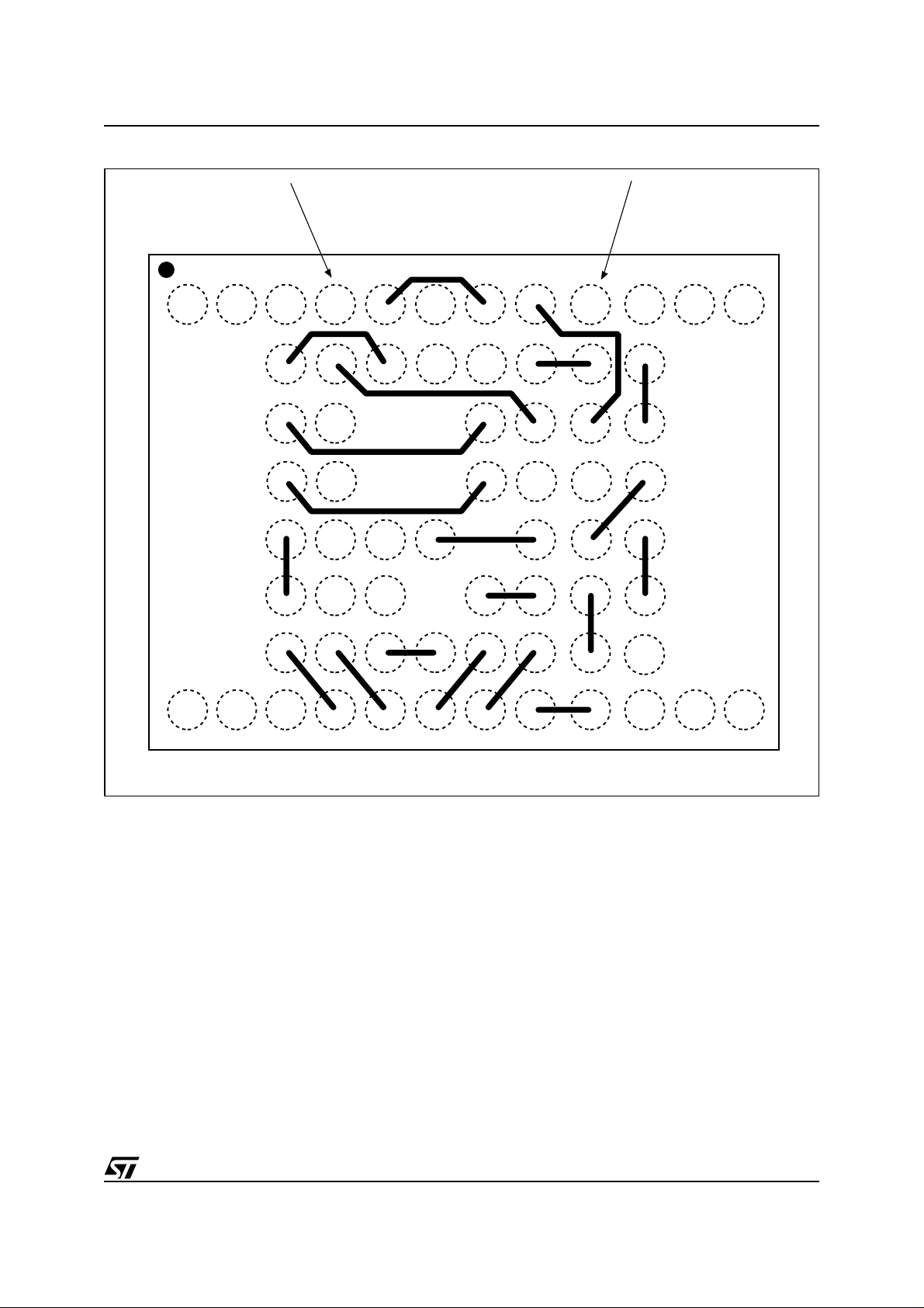
M36W432T, M36W432B
Figure 24. Stacked LFBGA66 Daisy Chain - PCB Connections proposal (Top view through package)
START
POINT
END
POINT
#1
A
B
C
D
E
F
G
32#2
4
87615
#4#3
H
AI05221
39/57

M36W432T, M36W432B
PART NUMBERING
Table 23. Ordering Informatio n Scheme
Example: M36W432T 70 ZA 6 T
Device Type
M36 = MMP (Flash + SRAM)
Operating Voltage
W=V
SRAM Chip Size & Organization
4 = 4 Mbit (256K x 16 bit)
Device Function
32 = 32 Mbit (x16), Boot Block
Array Matrix
T=TopBoot
B = Bottom Boot
Speed
70 = 70ns
85 = 85ns
= 2.7V to 3.3V, V
DDF
DDS=VDDQF
= 2.7V to 3.3V
Package
ZA = LFBGA66: 0.8mm pitch
Temperature Range
1 = 0 to 70°C
6 = –40 to 85°C
Option
T = Tape& Reel packing
Devices are shipped from the factory with the m emory content bits erased to ’1’.
Table 24. Daisy Chain Ordering Scheme
Example: M36W432 -ZA T
Device Type
M36W432
Daisy Chain
-ZA = LFBGA66: 0.8mm pitch
Option
T = Tape& Reel Packing
For a list of available options (Speed, Package, etc...) or for further infor mation on any aspect of this device, please contact the STMicroelectronics Sales Office nearest to you.
40/57

REVISION HISTORY
Table 25. Document Revision History
Date Version Revision Details
19-Jun-2001 -01 First Issue
16-Jul-2001 -02
11-Feb-2002 -03 Package mechanical data clarified (Table 22)
Flash Commands Table corrections: Protect/Lock, Unprotect/Unlock, Lock/LockDown
M36W432T, M36W432B
41/57

M36W432T, M36W432B
APPENDIX A. FLASH MEMORY BLOCK ADDRESS TABLES
Table 26. Top Boot Block Addresses,
M36W432T
#
0 4 1FF000-1FFFFF
1 4 1FE000-1FEFFF
2 4 1FD000-1FDFFF
3 4 1FC000-1FCFFF
4 4 1FB000-1FBFFF
5 4 1FA000-1FAFFF
6 4 1F9000-1F9FFF
7 4 1F8000-1F8FFF
8 32 1F0000-1F7FFF
9 32 1E8000-1EFFFF
10 32 1E0000-1E7FFF
11 32 1D8000-1DFFFF
12 32 1D0000-1D7FFF
13 32 1C8000-1CFFFF
14 32 1C0000-1C7FFF
15 32 1B8000-1BFFFF
16 32 1B0000-1B7FFF
17 32 1A8000-1AFFFF
18 32 1A0000-1A7FFF
19 32 198000-19FFFF
20 32 190000-197FFF
21 32 188000-18FFFF
22 32 180000-187FFF
23 32 178000-17FFFF
24 32 170000-177FFF
25 32 168000-16FFFF
26 32 160000-167FFF
27 32 158000-15FFFF
28 32 150000-157FFF
29 32 148000-14FFFF
30 32 140000-147FFF
31 32 138000-13FFFF
32 32 130000-137FFF
33 32 128000-12FFFF
Size
(KWord)
Address Range
34 32 120000-127FFF
35 32 118000-11FFFF
36 32 110000-117FFF
37 32 108000-10FFFF
38 32 100000-107FFF
39 32 0F8000-0FFFFF
40 32 0F0000-0F7FFF
41 32 0E8000-0EFFFF
42 32 0E0000-0E7FFF
43 32 0D8000-0DFFFF
44 32 0D0000-0D7FFF
45 32 0C8000-0CFFFF
46 32 0C0000-0C7FFF
47 32 0B8000-0BFFFF
48 32 0B0000-0B7FFF
49 32 0A8000-0AFFFF
50 32 0A0000-0A7FFF
51 32 098000-09FFFF
52 32 090000-097FFF
53 32 088000-08FFFF
54 32 080000-087FFF
55 32 078000-07FFFF
56 32 070000-077FFF
57 32 068000-06FFFF
58 32 060000-067FFF
59 32 058000-05FFFF
60 32 050000-057FFF
61 32 048000-04FFFF
62 32 040000-047FFF
63 32 038000-03FFFF
64 32 030000-037FFF
65 32 028000-02FFFF
66 32 020000-027FFF
67 32 018000-01FFFF
68 32 010000-017FFF
69 32 008000-00FFFF
70 32 000000-007FFF
42/57
M36W432T, M36W432B
Table 27. Bottom Boot Block Addresses,
M36W432B
#
70 32 1F8000-1FFFFF
69 32 1F0000-1F7FFF
68 32 1E8000-1EFFFF
67 32 1E0000-1E7FFF
66 32 1D8000-1DFFFF
65 32 1D0000-1D7FFF
64 32 1C8000-1CFFFF
63 32 1C0000-1C7FFF
62 32 1B8000-1BFFFF
61 32 1B0000-1B7FFF
60 32 1A8000-1AFFFF
59 32 1A0000-1A7FFF
58 32 198000-19FFFF
57 32 190000-197FFF
56 32 188000-18FFFF
55 32 180000-187FFF
54 32 178000-17FFFF
53 32 170000-177FFF
52 32 168000-16FFFF
51 32 160000-167FFF
50 32 158000-15FFFF
49 32 150000-157FFF
48 32 148000-14FFFF
47 32 140000-147FFF
46 32 138000-13FFFF
45 32 130000-137FFF
44 32 128000-12FFFF
43 32 120000-127FFF
42 32 118000-11FFFF
41 32 110000-117FFF
40 32 108000-10FFFF
39 32 100000-107FFF
38 32 0F8000-0FFFFF
37 32 0F0000-0F7FFF
Size
(KWord)
Address Range
36 32 0E8000-0EFFFF
35 32 0E0000-0E7FFF
34 32 0D8000-0DFFFF
33 32 0D0000-0D7FFF
32 32 0C8000-0CFFFF
31 32 0C0000-0C7FFF
30 32 0B8000-0BFFFF
29 32 0B0000-0B7FFF
28 32 0A8000-0AFFFF
27 32 0A0000-0A7FFF
26 32 098000-09FFFF
25 32 090000-097FFF
24 32 088000-08FFFF
23 32 080000-087FFF
22 32 078000-07FFFF
21 32 070000-077FFF
20 32 068000-06FFFF
19 32 060000-067FFF
18 32 058000-05FFFF
17 32 050000-057FFF
16 32 048000-04FFFF
15 32 040000-047FFF
14 32 038000-03FFFF
13 32 030000-037FFF
12 32 028000-02FFFF
11 32 020000-027FFF
10 32 018000-01FFFF
9 32 010000-017FFF
8 32 008000-00FFFF
7 4 007000-007FFF
6 4 006000-006FFF
5 4 005000-005FFF
4 4 004000-004FFF
3 4 003000-003FFF
2 4 002000-002FFF
1 4 001000-001FFF
0 4 000000-000FFF
43/57

M36W432T, M36W432B
APPENDIX B. CO MMO N FLASH INTERFACE (CFI)
TheCommonFlashInterfaceisaJEDECapproved, standardized data structure that can be
read from the Flash memory device. It allows a
system software to query the device to determine
various electrical and timing parameters, density
information and functions supported by the memory. The system can interface easily with the device, enabling the software to upgrade itself when
necessary.
When the CF I Query Command (RCFI) is issued
the device ent ers CFI Que ry mode and the data
Table 28. Query Structure Overview
Offset Sub-section Name Description
00h Reserved Reserved for algorithm-specific information
10h CFI Query Identification String Command set ID and algorithm data offset
1Bh System Interface Information Device timing & voltage information
27h Device Geometry Definition Flash device layout
P Primary Algorithm-specific Extended Query table
A Alternate Algorithm-specific Extended Query table
Note: Query dataarealways presented on the lowest order data outputs.
structure is read from the memory. T ables 28, 29,
30, 31, 32 and 33 show the addresses used to r etrieve the data.
The CFI data structure also contains a security
area where a 6 4 bit uni que security number is written (see Table 33, Security Code area). This area
can be accessed only in Read mode by the final
user. It is impossible to change the security number after it has been written by ST. Issue a Read
command to return to Read mode.
Additional information specific to the Primary
Algorithm (optional)
Additional information specific to the Alternate
Algorithm (optional)
Table 29. CFI Query Identification String
Offset Data Description Value
00h 0020h Manufacturer Code ST
01h
02h-0Fh reserved Reserved
10h 0051h "Q"
11h 0052h Query Unique ASCII String "QRY" "R"
12h 0059h "Y"
13h 0003h
14h 0000h
15h 0035h
16h 0000h
17h 0000h
18h 0000h
19h 0000h
1Ah 0000h
Note: Query data are always presented on the lowest order data outputs (DQ7-DQ0) only. DQ8-DQ15 are ‘0’.
88BAh
88BBh
Device Code
Primary Algorithm Command Set and Control Interface ID code 16 bit ID code
defining a specific algorithm
Address for Primary Algorithm extended Query table (see Table 31) P = 35h
Alternate Vendor Command Set and Control Interface ID Code second vendorspecified algorithm supported (0000h means none exists)
Address for Alternate Algorithm extended Query table
(0000h means none exists)
compatible
Top
Bottom
Intel
NA
NA
44/57

M36W432T, M36W432B
Table 30. CFI Query System Interface Information
Offset Data Description Value
Logic Supply Minimum Program/Erase or Write voltage
V
1Bh 0027h
1Ch 0036h
1Dh 00B4h
1Eh 00C6h
1Fh 0004h
20h 0004h
21h 000Ah
22h 0000h
23h 0005h
24h 0005h
25h 0003h
26h 0000h
DD
bit 7 to 4 BCD value in volts
bit 3 to 0 BCD value in 100 mV
Logic Supply Maximum Program/Erase or Write voltage
V
DD
bit 7 to 4 BCD value in volts
bit 3 to 0 BCD value in 100 mV
[Programming] Supply Minimum Program/Erase voltage
V
PP
bit 7 to 4 HEX value in volts
bit 3 to 0 BCD value in 100 mV
[Programming] Supply Maximum Program/Erase voltage
V
PP
bit 7 to 4 HEX value in volts
bit 3 to 0 BCD value in 100 mV
n
Typical timeout per single word program = 2
Typical timeout for Double Word Program = 2
Typical timeout per individual block erase = 2
Typical timeout for full chip erase = 2
n
Maximum timeout for word program = 2
Maximum timeout for Double Word Program = 2
Maximum timeout per individual block erase = 2
n
Maximum timeout for chip erase = 2
times typical
µs
n
n
ms
n
times typical
µs
ms
n
times typical
n
times typical
2.7V
3.6V
11.4V
12.6V
16µs
16µs
1s
NA
512µs
512µs
8s
NA
45/57

M36W432T, M36W432B
Table 31. Device Geometry Definition
Offset Word
Mode
27h 0016h
28h
29h
2Ah
2Bh
2Ch 0002h
2Dh
2Eh
2Fh
30h
31h
32h
M36W432T
33h
34h
2Dh
2Eh
2Fh
30h
31h
32h
M36W432B
33h
34h
Data Description Value
Device Size = 2
0001h
0000h
0002h
0000h
003Eh
0000h
0000h
0001h
0007h
0000h
0020h
0000h
0007h
0000h
0020h
0000h
003Eh
0000h
0000h
0001h
Flash Device Interface Code description
Maximum number of bytes in multi-byte program or page = 2
Number of Erase Block Regions within the device.
It specifies the number of regions within the device containing contiguous
Erase Blocks of the same size.
Region 1 Information
Number of identical-size erase block = 003Eh+1
Region 1 Information
Block size in Region 1 = 0100h * 256 byte
Region 2 Information
Number of identical-size erase block = 0007h+1
Region 2 Information
Block size in Region 2 = 0020h * 256 byte
Region 1 Information
Number of identical-size erase block = 0007h+1
Region 1 Information
Block size in Region 1 = 0020h * 256 byte
Region 2 Information
Number of identical-size erase block = 003Eh=1
Region 2 Information
Block size in Region 2 = 0100h * 256 byte
n
in number of bytes
4 MByte
x16
Async.
n
4
2
63
64 KByte
8
8 KByte
8
8 KByte
63
64 KByte
46/57

M36W432T, M36W432B
Table 32. Primary Algorithm-Specific Extended Query Table
Offset
P = 35h
(1)
(P+0)h = 35h 0050h
(P+1)h = 36h 0052h "R"
(P+2)h = 37h 0049h "I"
(P+3)h = 38h 0031h Major version number, ASCII "1"
(P+4)h = 39h 0030h Minor version number, ASCII "0"
Data Description Value
Primary Algorithm extended Query table unique ASCII string “PRI”
"P"
(P+5)h = 3Ah 0066h Extended Query table contents for Primary Algorithm. Address (P+5)h
(P+6)h = 3Bh 0000h
(P+7)h = 3Ch 0000h
(P+8)h = 3Dh 0000h
contains less significant byte.
bit 0 Chip Erase supported (1 = Yes, 0 = No)
bit 1 Suspend Erase supported (1 = Yes, 0 = No)
bit 2 Suspend Program supported (1 = Yes, 0 = No)
bit 3 Legacy Lock/Unlock supported (1 = Yes, 0 = No)
bit 4 Queued Erase supported (1 = Yes, 0 = No)
bit 5 Instant individual block locking supported (1 = Yes, 0 = No)
bit 6 Protection bits supported (1 = Yes, 0 = No)
bit 7 Page mode read supported (1 = Yes, 0 = No)
bit 8 Synchronous read supported (1 = Yes, 0 = No)
No
Yes
Yes
No
No
Yes
Yes
No
No
bit 31 to 9 Reserved; undefined bits are ‘0’
(P+9)h = 3Eh 0001h Supported Functions after Suspend
Read Array, Read Status Register and CFI Query are always supported
during Erase or Program operation
bit 0 Program supported after Erase Suspend (1 = Yes, 0 = No)
bit 7 to 1 Reserved; undefined bits are ‘0’ Yes
(P+A)h = 3Fh 0003h Block Lock Status : Defines which bits in the Block Status Register section of
(P+B)h = 40h 0000h
the Query are implemented.
Address (P+A)h contains less significant byte
bit 0 Block Lock Status bit active (1 = Yes, 0 = No)
(P+C)h = 41h 0030h V
bit 1 Block Lock-Down Status bit active (1 = Yes, 0 = No)
bit 15 to 2 Reserved for future use; undefined bits are ‘0’
Logic Supply Optimum Program/Erase voltage (highest performance)
DD
Yes
Yes
3V
bit 7 to 4 HEX value in volts
bit 3 to 0 BCD value in 100 mV
(P+D)h = 42h 00C0h V
Supply Optimum Program/Erase voltage
PP
12V
bit 7 to 4 HEX value in volts
bit 3 to 0 BCD value in 100 mV
(P+E)h = 43h 0001h Number of Protection register fields in JEDEC ID space.
01
"00h," indicates that 256 protection bytes are available
(P+F)h = 44h 0080h Protection Field 1: Protection Description
(P+10)h = 45h 0000h 00h
(P+11)h = 46h 0003h 8 Byte
(P+12)h = 47h 0003h 8 Byte
This field describes user-available. One Time Programmable (OTP)
Protection register bytes. Some are pre-programmed with device unique
serial numbers. Others are user programmable. Bits 0–15 point to the
Protection register Lock byte, the section’s first byte.
The following bytes are factory pre-programmed and user-programmable.
80h
bit 0 to 7 Lock/bytes JEDEC-plane physical low address
bit 8 to 15 Lock/bytes JEDEC-plane physical high address
n
bit 16 to 23 "n" such that 2
bit 24 to 31 "n" such that 2
= factory pre-programmed bytes
n
= user programmable bytes
(P+13)h = 48h Reserved
Note: 1. See Table 29, offset 15 for P pointer definition.
47/57

M36W432T, M36W432B
Table 33. Security Code Area
Offset Data Description
80h 00XX Protection Register Lock
81h XXXX
82h XXXX
83h XXXX
84h XXXX
85h XXXX
86h XXXX
87h XXXX
88h XXXX
64 bits: unique device number
64 bits: User Programmable OTP
48/57

APPENDIX C. FLASH MEMORY FLOWCHARTS AND PSEUDO CODES
Figure 25. Program Flowchart and Pseudo Code
Start
M36W432T, M36W432B
Write 40h or 10h
Write Address
& Data
Read Status
Register
b7 = 1
YES
b3 = 0
YES
b4 = 0
YES
b1 = 0
YES
End
NO
NO
NO
NO
V
PPF
Error (1, 2)
Error (1, 2)
Program to Protected
Block Error (1, 2)
Invalid
Program
program_command (addressToProgram, dataToProgram) {:
writeToFlash (any_address, 0x40) ;
/*or writeToFlash (any_address, 0x10) ; */
writeToFlash (addressToProgram, dataToProgram) ;
/*Memory enters read status state after
the Program Command*/
do {
status_register=readFlash (any_address) ;
/* EF or GF must be toggled*/
} while (status_register.b7== 0) ;
if (status_register.b3==1) /*V
error_handler ( ) ;
if (status_register.b4==1) /*program error */
error_handler ( ) ;
if (status_register.b1==1) /*program to protect block error */
error_handler ( ) ;
}
invalid error */
PPF
AI05222
Note: 1. Status check of b1 (Protected Block), b3 (V
a sequence.
2. If an error is found, the Status Register must be cleared before further Program/Erase Controller operations.
Invalid) and b4 (Program Error) canbe made aftereach programoperationor after
PPF
49/57

M36W432T, M36W432B
Figure 26. Double Word Program Flowchart and Pseudo Code
Start
Write 30h
Write Address 1
& Data 1 (3)
Write Address 2
& Data 2 (3)
Read Status
Register
b7 = 1
YES
b3 = 0
YES
b4 = 0
NO
NO
NO
V
Invalid
PPF
Error (1, 2)
Program
Error (1, 2)
double_word_program_command (addressToProgram1, dataToProgram1,
addressToProgram2, dataToProgram2)
{
writeToFlash (any_address, 0x30) ;
writeToFlash (addressToProgram1, dataToProgram1) ;
/*see note (3) */
writeToFlash (addressToProgram2, dataToProgram2) ;
/*see note (3) */
/*Memory enters read status state after
the Program command*/
do {
status_register=readFlash (any_address) ;
/* EF or GF must be toggled*/
} while (status_register.b7== 0) ;
if (status_register.b3==1) /*V
error_handler ( ) ;
if (status_register.b4==1) /*program error */
error_handler ( ) ;
invalid error */
PPF
YES
NO
b1 = 0
YES
End
Note: 1. Status check of b1 (Protected Block), b3 (V
a sequence.
2. If an error is found, the Status Register must be cleared before further Program/Erase operations.
3. Address 1 and Address 2 must be consecutive addresses differing only for bit A0.
Program to Protected
Block Error (1, 2)
PPF
if (status_register.b1==1) /*program to protect block error */
error_handler ( ) ;
}
Invalid) and b4 (Program Error) canbe made aftereach programoperationor after
50/57
AI05223

Figure 27. Program Suspend & Resume Flowchart and Pseudo Code
Start
program_suspend_command ( ) {
Write B0h
Write 70h
Read Status
Register
writeToFlash (any_address, 0xB0) ;
writeToFlash (any_address, 0x70) ;
/* read status register to check if
program has already completed */
do {
status_register=readFlash (any_address) ;
/* EF or GF must be toggled*/
M36W432T, M36W432B
b7 = 1
YES
b2 = 1
YES
Write FFh
Read data from
another address
Write D0h
Program Continues
NO
NO
Program Complete
Write FFh
Read Data
} while (status_register.b7== 0) ;
if (status_register.b2==0) /*program completed */
{ writeToFlash (any_address, 0xFF) ;
read_data ( ) ; /*read data from another block*/
/*The device returns to Read Array
(as if program/erase suspend was not issued).*/
}
else
{ writeToFlash (any_address, 0xFF) ;
read_data ( ); /*read data from another address*/
writeToFlash (any_address, 0xD0) ;
/*write 0xD0 to resume program*/
}
}
AI05224
51/57
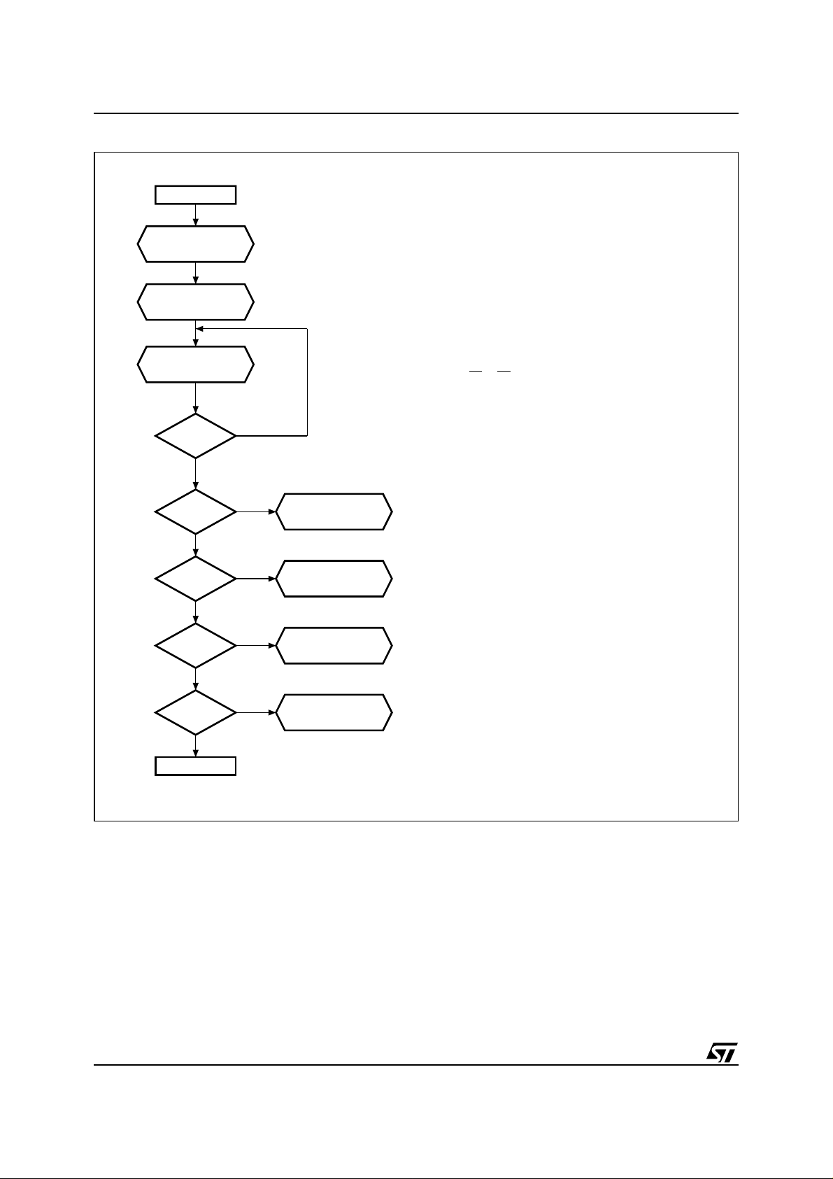
M36W432T, M36W432B
Figure 28. Erase Flowchart and Pseudo Code
Start
Write 20h
Write Block
Address & D0h
erase_command ( blockToErase ) {
writeToFlash (any_address, 0x20) ;
writeToFlash (blockToErase, 0xD0) ;
/* only A12-A20 are significannt */
/* Memory enters read status state after
the Erase Command */
Read Status
Register
YES
YES
NO
YES
YES
NO
NO
YES
NO
NO
V
PPF
Error (1)
Command
Sequence Error (1)
Erase to Protected
Block Error (1)
b7 = 1
b3 = 0
b4, b5 = 1
b5 = 0 Erase Error (1)
b1 = 0
End
Invalid
do {
status_register=readFlash (any_address) ;
/* EF or GF must be toggled*/
} while (status_register.b7== 0) ;
if (status_register.b3==1) /*V
error_handler ( ) ;
if ( (status_register.b4==1) && (status_register.b5==1) )
/* command sequence error */
error_handler ( ) ;
if ( (status_register.b5==1) )
/* erase error */
error_handler ( ) ;
if (status_register.b1==1) /*program to protect block error */
error_handler ( ) ;
}
invalid error */
PPF
AI05225
Note: If an error is found, the Status Register must be cleared before further Program/Erase operations.
52/57

Figure 29. Erase Suspend & Resume Flow chart and Pseudo Code
Start
Write B0h
erase_suspend_command ( ) {
writeToFlash (any_address, 0xB0) ;
M36W432T, M36W432B
Write 70h
Read Status
Register
b7 = 1
b6 = 1
Write FFh
Read data from
another block
Program/Protection Program
Block Protect/Unprotect/Lock
or
or
Write D0h
Erase Continues
NO
YES
NO
YES
Erase Complete
Write FFh
Read Data
writeToFlash (any_address, 0x70) ;
/* read status register to check if
erase has already completed */
{
status_register=readFlash (any_address) ;
/* EF or GF must be toggled*/
} while (status_register.b7== 1) ;
if (status_register.b6==1) /*erase completed */
{ writeToFlash (any_address, 0xFF) ;
read_data ( ) ; /*read data from another block*/
/*The device returns to Read Array
(as if program/erase suspend was not issued).*/
}
else
{ read_program_data ( );
/*read or program data from another address*/
writeToFlash (any_address, 0xD0) ;
/*write 0xD0 to resume erase*/
}
}
AI05226
53/57

M36W432T, M36W432B
Figure 30. Locking Operations Flowchart and Pseudo Code
Start
Write 60h
Write
01h, D0h or 2Fh
Write 90h
Read Status
Register
Locking
change
confirmed?
YES
Write FFh
End
NO
locking_operation_command (address, lock_operation) {
writeToFlash (any_address, 0x60) ; /*configuration setup*/
if (lock_operation==PROTECT) /*to protect the block*/
writeToFlash (address, 0x01) ;
else if (lock_operation==UNPROTECT) /*to unprotect the block*/
writeToFlash (address, 0xD0) ;
else if (lock_operation==LOCK) /*to lock the block*/
writeToFlash (address, 0x2F) ;
writeToFlash (any_address, 0x90) ;
if (readFlash (address) ! = locking_state_expected)
error_handler () ;
/*Check the locking state (see Read Block Signature table )*/
writeToFlash (any_address, 0xFF) ; /*Reset to Read Array mode*/
}
AI05227
54/57
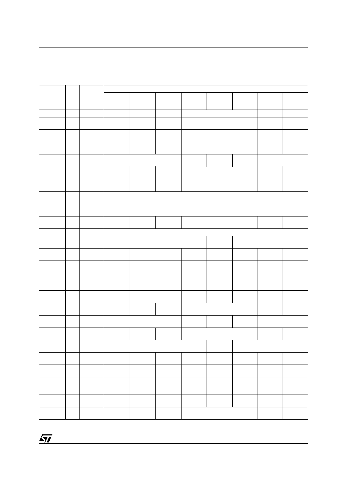
M36W432T, M36W432B
APPENDIX D. F LASH MEMORY COMMAND INTERFACE AND PROGRAM/ERASE CONTROLLER
STATE
Table 34. Write State Machine Current/Next, sheet 1 of 2
Current
StateSRbit 7
Read Array “1” Array Read Array Prog.Setup Ers. Setup Read Array Read Sts. Read Array
Read
Status
Read
Elect.Sg.
Read CFI
Query
Lock Setup “1” Status Lock Command Error
Lock Cmd
Error
Lock
(complete)
Prot. Prog.
Setup
Prot. Prog.
(continue)
Prot. Prog.
(complete)
Prog.Setup “1” Status Program
Program
(continue)
Prog.Sus
Status
Prog.Sus
Read Array
Prog.Sus
Read
Elect.Sg.
Prog.Sus
Read CFI
Program
(complete)
Erase
Setup
Erase
Cmd.Error
Erase
(continue)
Erase Sus
Read Sts
Erase Sus
Read Array
Erase Sus
Read
Elect.Sg.
Erase Sus
Read CFI
Erase
(complete)
Note: Cmd = Command, Elect.Sg. = Electronic Signature, Ers = Erase, Prog. = Program, Prot = Protection, Sus = Suspend.
Data
When
Read
“1” Status Read Array
Electronic
“1”
Signature
“1” CFI Read Array
“1” Status Read Array
“1” Status Read Array
“1” Status Protection Register Program
“0” Status Protection Register Program continue
“1” Status Read Array
“0” Status Program (continue)
“1” Status
“1” Array
Electronic
“1”
Signature
“1” CFI
“1” Status Read Array
“1” Status Erase Command Error
“1” Status Read Array
“0” Status Erase (continue)
“1” Status
“1” Array
Electronic
“1”
Signature
“1” CFI
“1” Status Read Array
Read
Array
(FFh)
Read Array
Prog. Sus
Read Array
Prog. Sus
Read Array
Prog. Sus
Read Array
Prog. Sus
Read Array
Erase Sus
Read Array
Erase Sus
Read Array
Erase Sus
Read Array
Erase Sus
Read Array
Program
Setup
(10/40h)
Program
Setup
Program
Setup
Program
Setup
Program
Setup
Program
Setup
Program
Setup
Program Suspend to
Read Array
Program Suspend to
Read Array
Program Suspend to
Read Array
Program Suspend to
Read Array
Program
Setup
Program
Setup
Program
Setup
Program
Setup
Program
Setup
Program
Setup
Program
Setup
Command Input (and Next State)
Erase
Setup
(10/40h)
Erase
Setup
Erase
Setup
Erase
Setup
Erase
Setup
Erase
Setup
Erase
Setup
Erase
Setup
Erase
Setup
Erase Sus
Read Array
Erase Sus
Read Array
Erase Sus
Read Array
Erase Sus
Read Array
Erase
Setup
Erase
Confirm
(D0h)
Lock
(complete)
Program
(continue)
Program
(continue)
Program
(continue)
Program
(continue)
Erase
(continue)
Erase
(continue)
Erase
(continue)
Erase
(continue)
Erase
(continue)
Prog/Ers
Suspend
(B0h)
Read Array
Read Array
Read Array
Lock Cmd
Error
Read Array
Read Array
Read Array
Prog. Sus
Read Sts
Prog. Sus
Read Array
Prog. Sus
Read Array
Prog. Sus
Read Array
Prog. Sus
Read Array
Read Array
Erase
CmdError
Read Array
Erase Sus
Read Sts
Erase Sus
Read Array
Erase Sus
Read Array
Erase Sus
Read Array
Erase Sus
Read Array
Read Array
Prog/Ers
Resume
(D0h)
Lock
(complete)
Program
(continue)
Program
(continue)
Program
(continue)
Program
(continue)
Erase
(continue)
Erase
(continue)
Erase
(continue)
Erase
(continue)
Erase
(continue)
Read
Status
(70h)
Read
Status
Read
Status
Read
Status
LockCommand Error
Read
Status
Read
Status
Read
Status
Program (continue)
Prog. Sus
Read Sts
Prog. Sus
Read Sts
Prog. Sus
Read Sts
Prog. Sus
Read Sts
Read
Status
Erase Command Error
Read
Status
Erase (continue)
Erase Sus
Read Sts
Erase Sus
Read Sts
Erase Sus
Read Sts
Erase Sus
Read Sts
Read
Status
Clear
Status
(50h)
Read Array
Read Array
Read Array
Read Array
Read Array
Read Array
Prog. Sus
Read Array
Prog. Sus
Read Array
Prog. Sus
Read Array
Prog. Sus
Read Array
Read Array
Read Array
Erase Sus
Read Array
Erase Sus
Read Array
Erase Sus
Read Array
Erase Sus
Read Array
Read Array
55/57

M36W432T, M36W432B
Table 35. Write State Machine Current/Next, sheet 2 of 2
Command Input (and Next State)
Current State
Read Array Read Elect.Sg. Read CFI Query Lock Setup
Read Status Read Elect.Sg. Read CFI Query LockSetup
Read Elect.Sg. Read Elect.Sg. Read CFI Query Lock Setup
Read CFI Query Read Elect.Sg. Read CFI Query Lock Setup
Lock Setup Lock Command Error Lock (complete)
Lock Cmd Error Read Elect.Sg. Read CFI Query Lock Setup
Lock (complete) Read Elect.Sg. Read CFI Query Lock Setup
Prot. Prog.
Setup
Prot. Prog.
(continue)
Prot. Prog.
(complete)
Prog. Setup Program
Program
(continue)
Prog.Suspend
Read Status
Prog.Suspend
Read Array
Prog.Suspend
ReadElect.Sg.
Prog.Suspend
Read CFI
Program
(complete)
EraseSetup EraseCommandError
Erase
Cmd.Error
Erase (continue) Erase (continue)
Erase Suspend
Read St stus
Erase Suspend
Read Array
Erase Suspend
ReadElect.Sg.
Erase Suspend
Read CFI Query
Erase
(complete)
Note: Cmd = Command, Elect.Sg. = Electronic Signature, Prog. = Program, Prot = Protection.
Read Elect.Sg.
(90h)
Read Elect.Sg. Read CFI Query Lock Setup
Prog. Suspend
Read Elect.Sg.
Prog. Suspend
Read Elect.Sg.
Prog. Suspend
Read Elect.Sg.
Prog. Suspend
Read Elect.Sg.
Read Elect.Sg. Read CFIQuery Lock Setup
Read Elect.Sg. Read CFI Query Lock Setup
Erase Suspend
Read Elect.Sg.
Erase Suspend
Read Elect.Sg.
Erase Suspend
Read Elect.Sg.
Erase Suspend
Read Elect.Sg.
Read Elect.Sg. Read CFI Query Lock Setup
Read CFI
Query
(98h)
Prog. Suspend
Read CFI Query
Prog. Suspend
Read CFI Query
Prog. Suspend
Read CFI Query
Prog. Suspend
Read CFI Query
Erase Suspend
Read CFI Query
Erase Suspend
Read CFI Query
Erase Suspend
Read CFI Query
Erase Suspend
Read CFI Query
Lock Setup
(60h)
Protection Register Program
Protection Register Program (continue)
LockSetup Erase Suspend Read Array
LockSetup Erase Suspend Read Array
LockSetup Erase Suspend Read Array
LockSetup Erase Suspend Read Array
Prot. Prog.
Setup (C0h)
Prot. Prog.
Setup
Prot. Prog.
Setup
Prot. Prog.
Setup
Prot. Prog.
Setup
Prot. Prog.
Setup
Prot. Prog.
Setup
Prot. Prog.
Setup
Program (continue)
Program Suspend ReadArray
Program Suspend ReadArray
Program Suspend ReadArray
Program Suspend ReadArray
Prot. Prog.
Setup
Prot. Prog.
Setup
Prot. Prog.
Setup
Lock Confirm
(01h)
Confirm (2Fh)
Lock Down
Read Array
Read Array
Read Array
Read Array
Read Array
Read Array
Read Array
Read Array
Read Array
Read Array
Unlock
Confirm
(D0h)
Program
(continue)
Program
(continue)
Program
(continue)
Program
(continue)
Erase
(continue)
Erase
(continue)
Erase
(continue)
Erase
(continue)
Erase
(continue)
56/57

M36W432T, M36W432B
Information furnished is believed to be accurate and reliable. However, STMicroelectronics assumes no responsibility for the consequences
of use of such information nor for any infringement of patents orother rights of third parties which may result from its use. No license is granted
by implication or otherwise under any patent or patent rights of STMicroelectronics. Specifications mentioned in this publication are subject
to change without notice. This publication supersedes and replaces all information previously supplied. STMicroelectronics products are not
authorized for use as critical components in life support devices or systems without express written approval of STMicroelectronics.
The ST logo is registered trademark of STMicroelectronics
All other names are the property of their respective owners.
2002 STMicroelectronics - All Rights Reserved
Australia - Brazil - China - Finland - France - Germany - Hong Kong - India - Italy - Japan - Malaysia - Malta - Morocco -
Singapore - Spain - Sweden - Switzerland - United Kingdom - U.S.A.
STMicroelectronics GROUP OF COMPANIES
www.st.com
57/57
 Loading...