

SGS Thomson Microelectronics M36W432TG, M36W432BG Datasheet

32 Mbit (2Mb x16, Boot Block) Flash Memory
and 4 Mbit (256Kb x16) SRAM, Multiple Memory Product
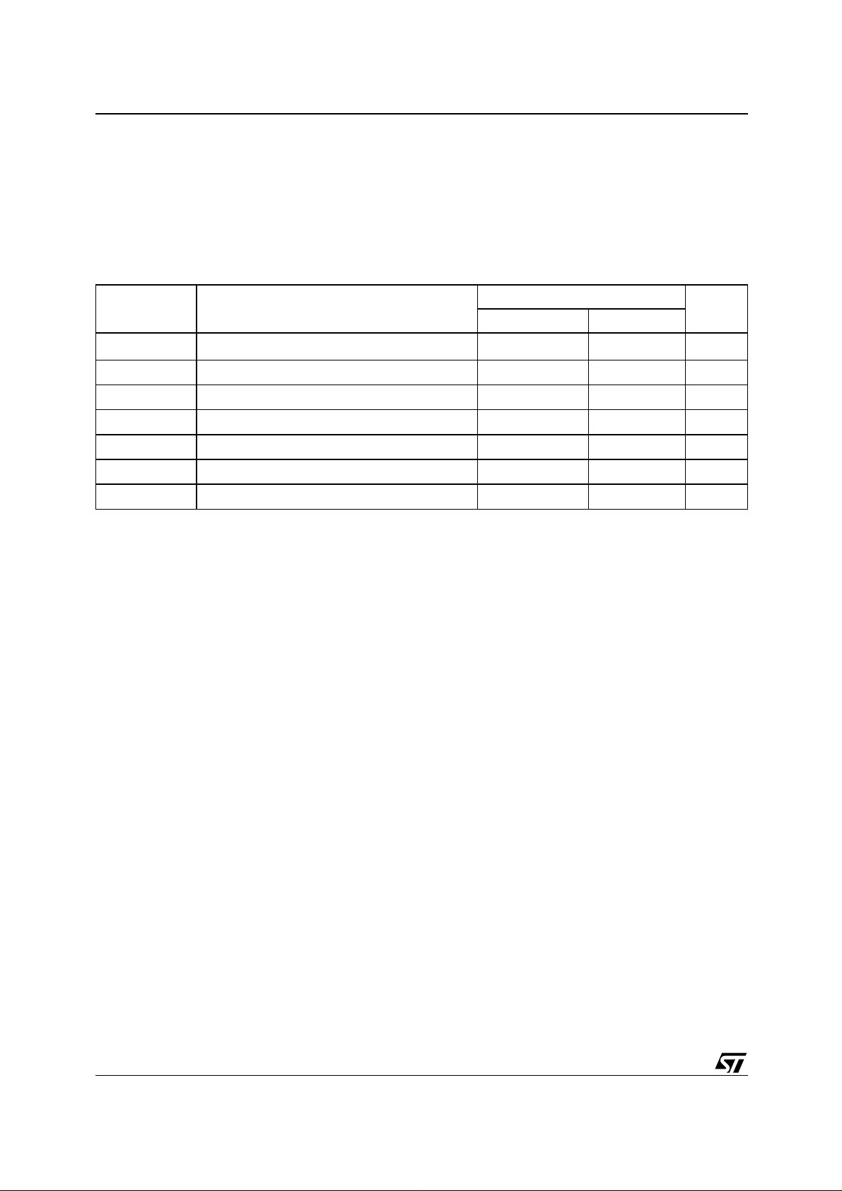
FEATURES SUMMARY
■ MULTIPLE MEMORY PRODUCT
– 32 Mbit (2Mb x 16), Boot Block, Flash Memory
– 4 Mbit (256Kb x 16) SRAM Memory
■ SUPPLY VOLTAGE
–V
–V
–V
■ ACCESS TIME: 70ns, 85ns
■ LOW POWER CONSUMPTION
■ ELECTRONIC SIGNATURE
– Manufacturer Code: 20h
– Top Device Code, M36W432TG: 88BAh
– Bottom Device Code, M36W432BG: 88BBh
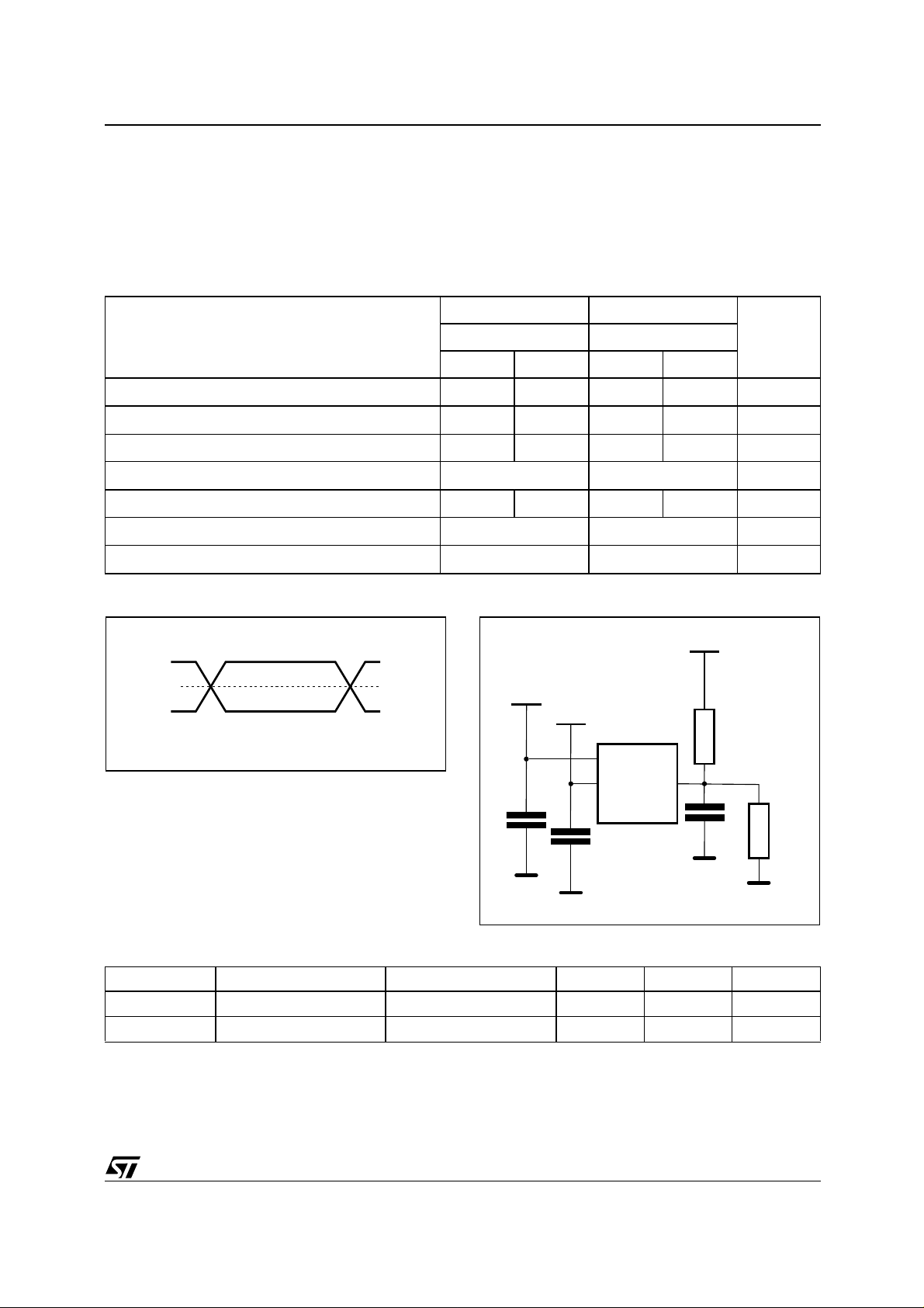
FLASH MEMORY
■ MEMORY BLOCKS
– Parameter Blocks (Top or Bottom Location)
– Main Blocks
■ PROGRAMMING TIME
– 10µs typical
– Double Word Programming Option
– Quadruple Word Programming Option
■ BLOCK LOCKING
– All blocks locked at Power up
– Any combination of blocks can be locked
–WP
■ AUTOMATIC STANDBY MODE
■ PROGRAM and ERASE SUSPEND
■ 100,000 PROGRAM/ERASE CYCLES per
BLOCK
■ COMMON FLASH INTERFACE
■ SECURITY
– 128 bit user programmable OTP cells
– 64 bit unique device identifier
= 2.7V to 3.3V
DDF
= V
DDS
= 12V for Fast Program (optional)
PPF
for Block Lock-Down
F
= 2.7V to 3.3V
DDQF
M36W432TG
M36W432BG
PRELIMINARY DATA
SRAM
■ 4 Mbit (256Kb x 16)
■ ACCESS TIME: 70ns
■ LOW V
■ POWER DOWN FEATURES USING TWO
CHIP ENABLE INPUTS
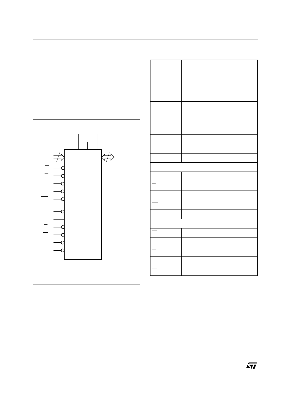
Figure 1. Package
DATA RETENTION: 1.5V
DDS
FBGA
Stacked LFBGA66 (ZA)
12 x 8 mm
November 2002
This is preliminary information on a new product now in development or undergoing evaluation. Details are subject to change without notice.
1/66

M36W432TG, M36W432BG
TABLE OF CONTENTS
SUMMARY DESCRIPTION. . . . . . . . . . . . . . . . . . . . . . . . . . . . . . . . . . . . . . . . . . . . . . . . . . . . . . . . . . . 6
Figure 2. Logic Diagram . . . . . . . . . . . . . . . . . . . . . . . . . . . . . . . . . . . . . . . . . . . . . . . . . . . . . . . . . . 6
Table 1. Signal Names . . . . . . . . . . . . . . . . . . . . . . . . . . . . . . . . . . . . . . . . . . . . . . . . . . . . . . . . . . . 6
Figure 3. LFBGA Connections (Top view through package). . . . . . . . . . . . . . . . . . . . . . . . . . . . . . . 7
SIGNAL DESCRIPTION . . . . . . . . . . . . . . . . . . . . . . . . . . . . . . . . . . . . . . . . . . . . . . . . . . . . . . . . . . . . . 8
Address Inputs (A0-A17). . . . . . . . . . . . . . . . . . . . . . . . . . . . . . . . . . . . . . . . . . . . . . . . . . . . . . . . . . 8
Address Inputs (A18-A20). . . . . . . . . . . . . . . . . . . . . . . . . . . . . . . . . . . . . . . . . . . . . . . . . . . . . . . . . 8
Data Input/Output (DQ0-DQ15). . . . . . . . . . . . . . . . . . . . . . . . . . . . . . . . . . . . . . . . . . . . . . . . . . . . . 8
Flash Chip Enable (EF). . . . . . . . . . . . . . . . . . . . . . . . . . . . . . . . . . . . . . . . . . . . . . . . . . . . . . . . . . . 8
Flash Output Enable (GF). . . . . . . . . . . . . . . . . . . . . . . . . . . . . . . . . . . . . . . . . . . . . . . . . . . . . . . . . 8
Flash Write Enable (WF). . . . . . . . . . . . . . . . . . . . . . . . . . . . . . . . . . . . . . . . . . . . . . . . . . . . . . . . . . 8
Flash Write Protect (WPF). . . . . . . . . . . . . . . . . . . . . . . . . . . . . . . . . . . . . . . . . . . . . . . . . . . . . . . . . 8
Flash Reset (RPF). . . . . . . . . . . . . . . . . . . . . . . . . . . . . . . . . . . . . . . . . . . . . . . . . . . . . . . . . . . . . . . 8
SRAM Chip Enable (E1S, E2S). . . . . . . . . . . . . . . . . . . . . . . . . . . . . . . . . . . . . . . . . . . . . . . . . . . . . 8
SRAM Write Enable (WS). . . . . . . . . . . . . . . . . . . . . . . . . . . . . . . . . . . . . . . . . . . . . . . . . . . . . . . . . 8
SRAM Output Enable (GS).. . . . . . . . . . . . . . . . . . . . . . . . . . . . . . . . . . . . . . . . . . . . . . . . . . . . . . . . 8
SRAM Upper Byte Enable (UBS). . . . . . . . . . . . . . . . . . . . . . . . . . . . . . . . . . . . . . . . . . . . . . . . . . . . 8
SRAM Lower Byte Enable (LBS). . . . . . . . . . . . . . . . . . . . . . . . . . . . . . . . . . . . . . . . . . . . . . . . . . . . 8
V
Supply Voltage (2.7V to 3.3V).. . . . . . . . . . . . . . . . . . . . . . . . . . . . . . . . . . . . . . . . . . . . . . . . . 8
DDF
and V
V
DDQF
V
Program Supply Voltage. . . . . . . . . . . . . . . . . . . . . . . . . . . . . . . . . . . . . . . . . . . . . . . . . . . . . . 8
PPF
V
and V
SSF
Supply Voltage (2.7V to 3.3V). . . . . . . . . . . . . . . . . . . . . . . . . . . . . . . . . . . . . . . . 8
DDS
Ground.. . . . . . . . . . . . . . . . . . . . . . . . . . . . . . . . . . . . . . . . . . . . . . . . . . . . . . . . . . . 9
SSS
FUNCTIONAL DESCRIPTION . . . . . . . . . . . . . . . . . . . . . . . . . . . . . . . . . . . . . . . . . . . . . . . . . . . . . . . 10
Figure 4. Functional Block Diagram . . . . . . . . . . . . . . . . . . . . . . . . . . . . . . . . . . . . . . . . . . . . . . . . 1 0
Table 2. Main Operation Modes . . . . . . . . . . . . . . . . . . . . . . . . . . . . . . . . . . . . . . . . . . . . . . . . . . . 11
MAXIMUM RATING. . . . . . . . . . . . . . . . . . . . . . . . . . . . . . . . . . . . . . . . . . . . . . . . . . . . . . . . . . . . . . . . 12
Table 3. Absolute Maximum Ratings. . . . . . . . . . . . . . . . . . . . . . . . . . . . . . . . . . . . . . . . . . . . . . . .12
DC AND AC PARAMETERS. . . . . . . . . . . . . . . . . . . . . . . . . . . . . . . . . . . . . . . . . . . . . . . . . . . . . . . . . 13
Table 4. Operating and AC Measurement Conditions. . . . . . . . . . . . . . . . . . . . . . . . . . . . . . . . . . . 13
Figure 5. AC Measurement I/O Waveform . . . . . . . . . . . . . . . . . . . . . . . . . . . . . . . . . . . . . . . . . . . 13
Figure 6. AC Measurement Load Circuit . . . . . . . . . . . . . . . . . . . . . . . . . . . . . . . . . . . . . . . . . . . . .13
Table 5. Device Capaci ta n ce. . . . . . . . . . . . . . . . . . . . . . . . . . . . . . . . . . . . . . . . . . . . . . . . . . . . . . 13
Table 6. DC Character i stics. . . . . . . . . . . . . . . . . . . . . . . . . . . . . . . . . . . . . . . . . . . . . . . . . . . . . . . 14
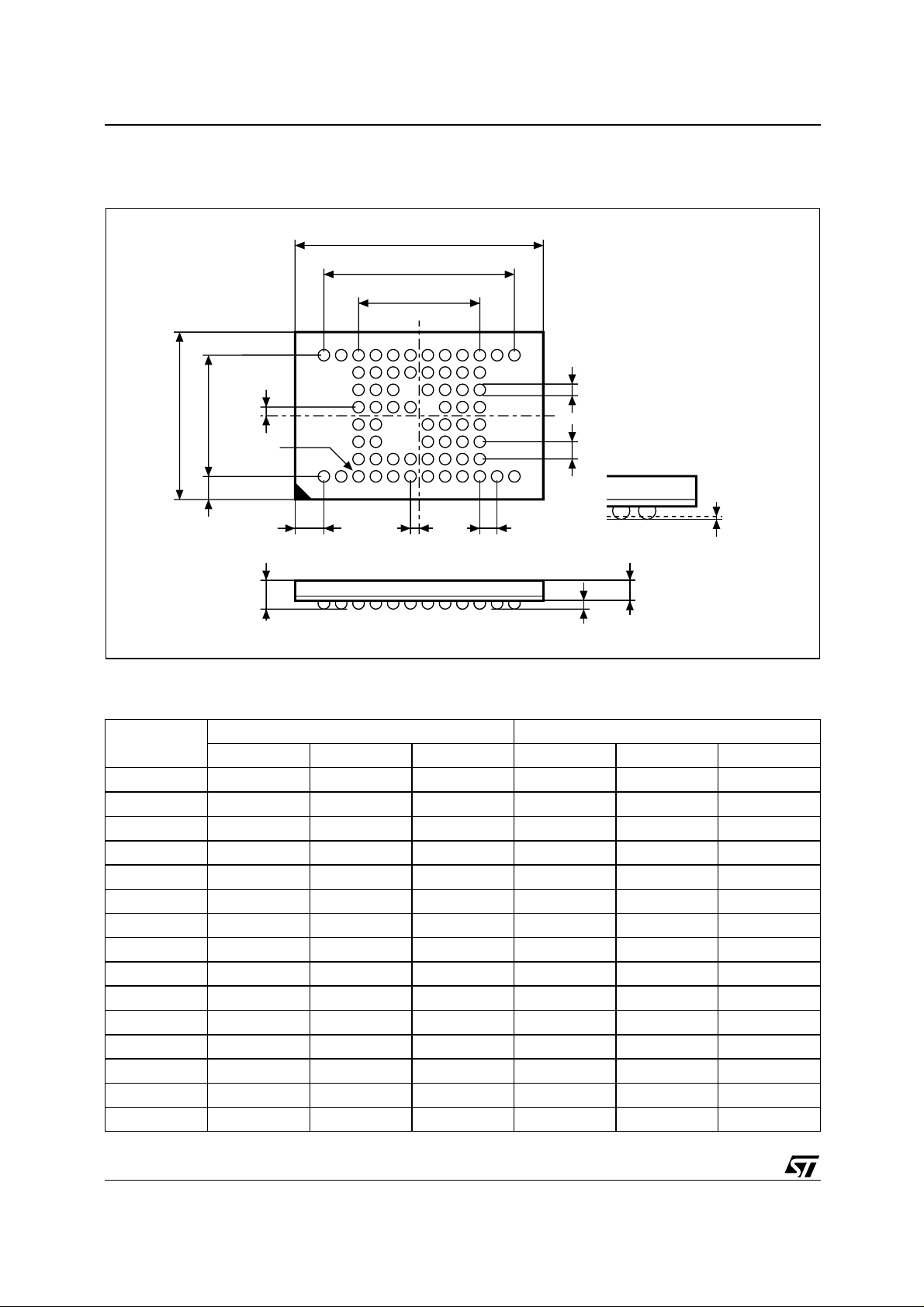
PACKAGE MECHANICAL . . . . . . . . . . . . . . . . . . . . . . . . . . . . . . . . . . . . . . . . . . . . . . . . . . . . . . . . . . 1 6
Figure 7. Stacked LFBGA66 12x8mm , 8x8 ball array, 0.8mm pitch, Bottom View Package Out line16
Table 7. Stacked LFBGA66 12x8mm, 8x8 ball array, 0.8mm pitch, Package Mecha nical Dat a . . . 16
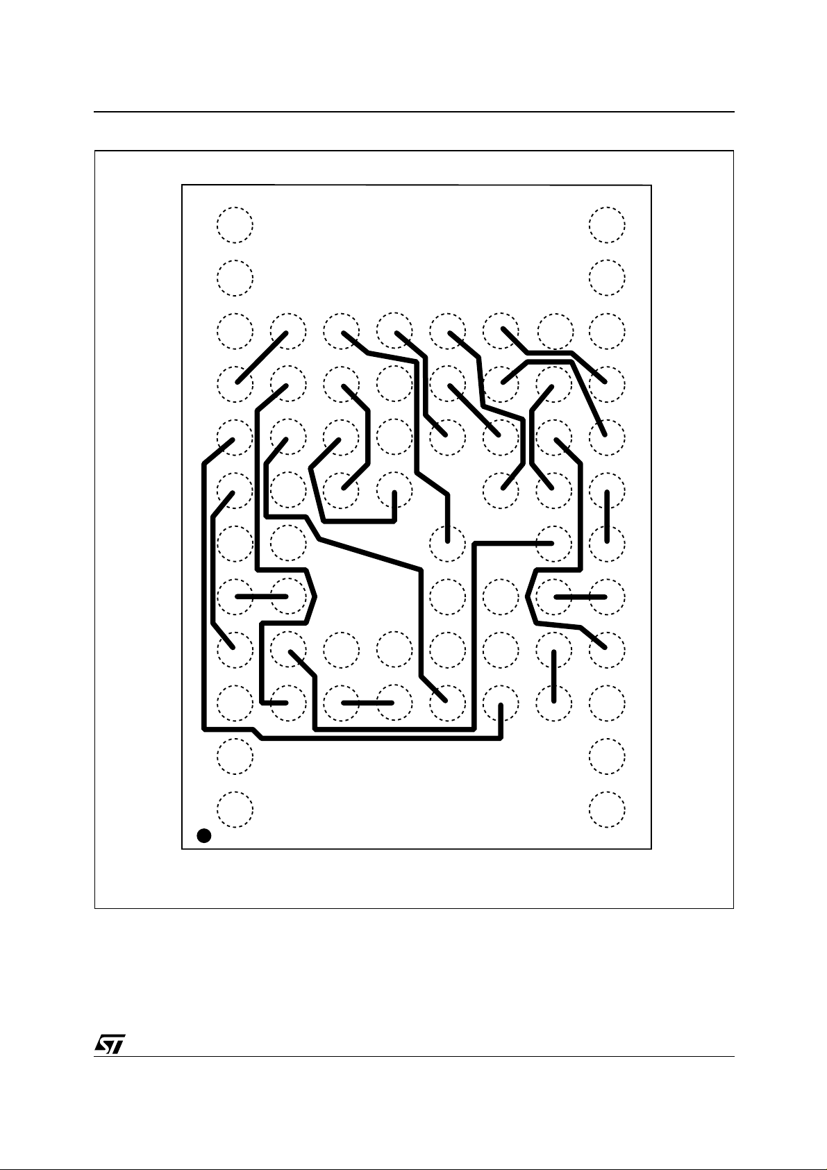
Figure 8. Stacked LFBGA66 Daisy Chain - Package Connections (Top view through package) . . 17
Figure 9. Stac k ed LFBGA6 6 Daisy C hain - PC B Connect ions proposal (Top view through package).18
2/66

M36W432TG, M36W432BG
PART NUMBERING . . . . . . . . . . . . . . . . . . . . . . . . . . . . . . . . . . . . . . . . . . . . . . . . . . . . . . . . . . . . . . . 19
Table 8. Ordering Information Scheme . . . . . . . . . . . . . . . . . . . . . . . . . . . . . . . . . . . . . . . . . . . . . . 19
Table 9. Daisy Chain Orde r ing Scheme . . . . . . . . . . . . . . . . . . . . . . . . . . . . . . . . . . . . . . . . . . . . . 19
FLASH DEVICE. . . . . . . . . . . . . . . . . . . . . . . . . . . . . . . . . . . . . . . . . . . . . . . . . . . . . . . . . . . . . . . . . . . 2 0
FLASH SUMMARY DESCRIPTION. . . . . . . . . . . . . . . . . . . . . . . . . . . . . . . . . . . . . . . . . . . . . . . . 20
Figure 10. Flash Block Ad d re sse s . . . . . . . . . . . . . . . . . . . . . . . . . . . . . . . . . . . . . . . . . . . . . . 21
Figure 11. Protect ion Regi ster Memory Map. . . . . . . . . . . . . . . . . . . . . . . . . . . . . . . . . . . . . . . 21
FLASH BUS OPERATIONS. . . . . . . . . . . . . . . . . . . . . . . . . . . . . . . . . . . . . . . . . . . . . . . . . . . . . . 22
Read.. . . . . . . . . . . . . . . . . . . . . . . . . . . . . . . . . . . . . . . . . . . . . . . . . . . . . . . . . . . . . . . . . . . . . 22
Write.. . . . . . . . . . . . . . . . . . . . . . . . . . . . . . . . . . . . . . . . . . . . . . . . . . . . . . . . . . . . . . . . . . . . . 22
Output Disable.. . . . . . . . . . . . . . . . . . . . . . . . . . . . . . . . . . . . . . . . . . . . . . . . . . . . . . . . . . . . . 22
Standby. . . . . . . . . . . . . . . . . . . . . . . . . . . . . . . . . . . . . . . . . . . . . . . . . . . . . . . . . . . . . . . . . . . 22
Automatic Standby.. . . . . . . . . . . . . . . . . . . . . . . . . . . . . . . . . . . . . . . . . . . . . . . . . . . . . . . . . . 22
Reset. . . . . . . . . . . . . . . . . . . . . . . . . . . . . . . . . . . . . . . . . . . . . . . . . . . . . . . . . . . . . . . . . . . . . 2 2
FLASH COMMAND INTERFACE. . . . . . . . . . . . . . . . . . . . . . . . . . . . . . . . . . . . . . . . . . . . . . . . . . 23
Read Memory Array Command. . . . . . . . . . . . . . . . . . . . . . . . . . . . . . . . . . . . . . . . . . . . . . . . . . . .23
Read Status Register Command. . . . . . . . . . . . . . . . . . . . . . . . . . . . . . . . . . . . . . . . . . . . . . . . . . .23
Read Electronic Signature Comma nd . . . . . . . . . . . . . . . . . . . . . . . . . . . . . . . . . . . . . . . . . . . . . . . 23
Read CFI Query Command. . . . . . . . . . . . . . . . . . . . . . . . . . . . . . . . . . . . . . . . . . . . . . . . . . . . . . . 23
Block Erase Command . . . . . . . . . . . . . . . . . . . . . . . . . . . . . . . . . . . . . . . . . . . . . . . . . . . . . . . . . . 23
Program Command. . . . . . . . . . . . . . . . . . . . . . . . . . . . . . . . . . . . . . . . . . . . . . . . . . . . . . . . . . . . . 24
Double Word Program Command . . . . . . . . . . . . . . . . . . . . . . . . . . . . . . . . . . . . . . . . . . . . . . . . . . 24
Clear Status Regist e r Command. . . . . . . . . . . . . . . . . . . . . . . . . . . . . . . . . . . . . . . . . . . . . . . . . . . 24
Program/Erase Suspend Comm and . . . . . . . . . . . . . . . . . . . . . . . . . . . . . . . . . . . . . . . . . . . . . . . . 24
Program/Eras e Resume Command . . . . . . . . . . . . . . . . . . . . . . . . . . . . . . . . . . . . . . . . . . . . . . . . 25
Protection Regi ste r Pr o g ra m Comman d . . . . . . . . . . . . . . . . . . . . . . . . . . . . . . . . . . . . . . . . . . . . . 25
Block Lock Command . . . . . . . . . . . . . . . . . . . . . . . . . . . . . . . . . . . . . . . . . . . . . . . . . . . . . . . . . . . 25
Block Unlock Command . . . . . . . . . . . . . . . . . . . . . . . . . . . . . . . . . . . . . . . . . . . . . . . . . . . . . . . . . 25
Block Lock-Down Command. . . . . . . . . . . . . . . . . . . . . . . . . . . . . . . . . . . . . . . . . . . . . . . . . . . . . . 25
Table 10. Flash Command Codes . . . . . . . . . . . . . . . . . . . . . . . . . . . . . . . . . . . . . . . . . . . . . . 23
Table 12. Flash Read Electronic Signature. . . . . . . . . . . . . . . . . . . . . . . . . . . . . . . . . . . . . . . . 27
Table 13. Flash Read Block Lock Signature. . . . . . . . . . . . . . . . . . . . . . . . . . . . . . . . . . . . . . . 27
Table 14. Flash Read Protection Register and Lock Register . . . . . . . . . . . . . . . . . . . . . . . . . 27
Table 15. Flash Program, Erase Times and Program/Erase Endurance Cycles . . . . . . . . . . . 28
FLASH BLOCK LOCKING . . . . . . . . . . . . . . . . . . . . . . . . . . . . . . . . . . . . . . . . . . . . . . . . . . . . . .29
Reading a Block’s Lock Status . . . . . . . . . . . . . . . . . . . . . . . . . . . . . . . . . . . . . . . . . . . . . . . . . . . . 29
Locked State . . . . . . . . . . . . . . . . . . . . . . . . . . . . . . . . . . . . . . . . . . . . . . . . . . . . . . . . . . . . . . . . . . 29
Unlocked State . . . . . . . . . . . . . . . . . . . . . . . . . . . . . . . . . . . . . . . . . . . . . . . . . . . . . . . . . . . . . . . . 2 9
Lock-Down State. . . . . . . . . . . . . . . . . . . . . . . . . . . . . . . . . . . . . . . . . . . . . . . . . . . . . . . . . . . . . . . 29
Locking Operatio n s Durin g Erase Su sp e nd . . . . . . . . . . . . . . . . . . . . . . . . . . . . . . . . . . . . . . . . . . 29
Table 16. Flash Block Lock Status . . . . . . . . . . . . . . . . . . . . . . . . . . . . . . . . . . . . . . . . . . . . . .30
Table 17. Flash Protection Status. . . . . . . . . . . . . . . . . . . . . . . . . . . . . . . . . . . . . . . . . . . . . . . 30
3/66

M36W432TG, M36W432BG
FLASH STATUS REGISTER . . . . . . . . . . . . . . . . . . . . . . . . . . . . . . . . . . . . . . . . . . . . . . . . . . . . . 31
Program/Erase Controller Status (Bit 7) . . . . . . . . . . . . . . . . . . . . . . . . . . . . . . . . . . . . . . . . . .31
Erase Suspend Status (Bit 6) . . . . . . . . . . . . . . . . . . . . . . . . . . . . . . . . . . . . . . . . . . . . . . . . . .31
Erase Status (Bit 5). . . . . . . . . . . . . . . . . . . . . . . . . . . . . . . . . . . . . . . . . . . . . . . . . . . . . . . . . . 3 1
Program Status (Bit 4). . . . . . . . . . . . . . . . . . . . . . . . . . . . . . . . . . . . . . . . . . . . . . . . . . . . . . . . 31
V
Status (Bit 3) . . . . . . . . . . . . . . . . . . . . . . . . . . . . . . . . . . . . . . . . . . . . . . . . . . . . . . . . . . 3 1
PPF
Program Suspend Status (Bit 2). . . . . . . . . . . . . . . . . . . . . . . . . . . . . . . . . . . . . . . . . . . . . . . . 31
Block Protection Status (Bit 1) . . . . . . . . . . . . . . . . . . . . . . . . . . . . . . . . . . . . . . . . . . . . . . . . .32
Reserved (Bit 0) . . . . . . . . . . . . . . . . . . . . . . . . . . . . . . . . . . . . . . . . . . . . . . . . . . . . . . . . . . . . 3 2
Table 18. Flash Status Register Bits. . . . . . . . . . . . . . . . . . . . . . . . . . . . . . . . . . . . . . . . . . . . . 32
Figure 12. Flash Read Mode AC Waveforms . . . . . . . . . . . . . . . . . . . . . . . . . . . . . . . . . . . . . . 33
Table 19. Flash Read AC Characteristics. . . . . . . . . . . . . . . . . . . . . . . . . . . . . . . . . . . . . . . . . 33
Figure 13. Flash Write AC Wavefo r ms, Write Enable Control l e d . . . . . . . . . . . . . . . . . . . . . . . 34
Table 20. Flash Write AC Chara cte ristics, Write En a ble Controlled. . . . . . . . . . . . . . . . . . . . . 35
Figure 14. Flash Write AC Waveforms, Chip Enable Controlled . . . . . . . . . . . . . . . . . . . . . . . . 36
Table 21. Flash Write AC Characteristics, Chip Enable Controlled . . . . . . . . . . . . . . . . . . . . . 37
Figu r e 1 5 . Flash Power -Up an d R e set AC W a veforms. . . . . . . . . . . . . . . . . . . . . . . . . . . . . . . 38
Table 22. Flash Power-Up and Reset AC Characteristics . . . . . . . . . . . . . . . . . . . . . . . . . . . . 38
SRAM DEVICE . . . . . . . . . . . . . . . . . . . . . . . . . . . . . . . . . . . . . . . . . . . . . . . . . . . . . . . . . . . . . . . . . . . 39
SRAM SUMMARY DESCRIPTION. . . . . . . . . . . . . . . . . . . . . . . . . . . . . . . . . . . . . . . . . . . . . . . . . 39
Figure 16. SRAM Logic Diagram . . . . . . . . . . . . . . . . . . . . . . . . . . . . . . . . . . . . . . . . . . . . . . . 39
SRAM OPERATIONS. . . . . . . . . . . . . . . . . . . . . . . . . . . . . . . . . . . . . . . . . . . . . . . . . . . . . . . . . . . 40
Read . . . . . . . . . . . . . . . . . . . . . . . . . . . . . . . . . . . . . . . . . . . . . . . . . . . . . . . . . . . . . . . . . . . . . 40
Write . . . . . . . . . . . . . . . . . . . . . . . . . . . . . . . . . . . . . . . . . . . . . . . . . . . . . . . . . . . . . . . . . . . . . 4 0
Standby/Power-Down . . . . . . . . . . . . . . . . . . . . . . . . . . . . . . . . . . . . . . . . . . . . . . . . . . . . . . . .40
Data Retention . . . . . . . . . . . . . . . . . . . . . . . . . . . . . . . . . . . . . . . . . . . . . . . . . . . . . . . . . . . . . 40
Output Disable . . . . . . . . . . . . . . . . . . . . . . . . . . . . . . . . . . . . . . . . . . . . . . . . . . . . . . . . . . . . . 40
Figure 17. SRAM Read Mode AC Waveforms, Address Controlled. . . . . . . . . . . . . . . . . . . . . 41
Figure 18. SRAM Read AC Waveforms, GS Controlled . . . . . . . . . . . . . . . . . . . . . . . . . . . . . . 41
Figure 19. SRAM Standby AC Waveforms . . . . . . . . . . . . . . . . . . . . . . . . . . . . . . . . . . . . . . . . 41
Table 23. SRAM Read AC Characteristics . . . . . . . . . . . . . . . . . . . . . . . . . . . . . . . . . . . . . . . .42
Figure 20. SRAM Write AC Waveforms, WS Controlled. . . . . . . . . . . . . . . . . . . . . . . . . . . . . . 43
Figu r e 2 1 . SRAM Write A C Wav e forms, E1S Con trolle d . . . . . . . . . . . . . . . . . . . . . . . . . . . . . 44
Figure 22. SRAM Write AC Waveforms, WS Controlled with GS Low . . . . . . . . . . . . . . . . . . . 45
Figure 23. SRAM Write Cycle Waveform, UBS and LBS Controlled, GS Low . . . . . . . . . . . . . 45
Table 24. SRAM Write AC Characteristics . . . . . . . . . . . . . . . . . . . . . . . . . . . . . . . . . . . . . . . . 46
Figure 24. SRAM Low V
Table 25. SRAM Low V
Data Retention AC Waveforms, E1S or UBS / LBS Controlled . . 47
DDS
Data Retention Characte r i stic. . . . . . . . . . . . . . . . . . . . . . . . . . . . 47
DDS
APPENDIX A. FLASH BLOCK ADDRESS TABLES. . . . . . . . . . . . . . . . . . . . . . . . . . . . . . . . . . . . . . 48
Table 26. Top Boot Block Addresses, M36W432TG. . . . . . . . . . . . . . . . . . . . . . . . . . . . . . . . . . . . 48
Table 27. Botto m Boo t Bl oc k Addre sse s, M36W432BG . . . . . . . . . . . . . . . . . . . . . . . . . . . . . . . . . 49
4/66

M36W432TG, M36W432BG
APPENDIX B. COMMON FLASH INTERFACE (CFI) . . . . . . . . . . . . . . . . . . . . . . . . . . . . . . . . . . . . . 50
Table 28. Query Stru cture Overview. . . . . . . . . . . . . . . . . . . . . . . . . . . . . . . . . . . . . . . . . . . . . . . .50
Table 29. CFI Query Identification String . . . . . . . . . . . . . . . . . . . . . . . . . . . . . . . . . . . . . . . . . . . .50
Table 30. CFI Query System Interface Information. . . . . . . . . . . . . . . . . . . . . . . . . . . . . . . . . . . . . 51
Table 31. Device Geome try Definition. . . . . . . . . . . . . . . . . . . . . . . . . . . . . . . . . . . . . . . . . . . . . . .52
Table 32. Primary Algorithm-Specific Extended Query Table . . . . . . . . . . . . . . . . . . . . . . . . . . . . . 53
Table 33. Security Code Area . . . . . . . . . . . . . . . . . . . . . . . . . . . . . . . . . . . . . . . . . . . . . . . . . . . . . 54
APPENDIX C. FLASH FLOWCHARTS AND PSEUDO CODES . . . . . . . . . . . . . . . . . . . . . . . . . . . . . 55
Figure 25. Flash Program Flowchart and Pseudo Code . . . . . . . . . . . . . . . . . . . . . . . . . . . . . . . . . 55
Figure 26. Double Word Program Flowchart and Pseudo Code . . . . . . . . . . . . . . . . . . . . . . . . . . . 56
Figure 28. Program Suspend & Resume Flowchart and Pseudo Code . . . . . . . . . . . . . . . . . . . . . 58
Figure 29. Erase Flowchart and Pseudo Code . . . . . . . . . . . . . . . . . . . . . . . . . . . . . . . . . . . . . . . . 59
Figure 30. Erase Suspend & Resume Flowchart and Pseudo Code. . . . . . . . . . . . . . . . . . . . . . . . 60
Figure 31. Locking Operations Flowchart and Pseudo Code . . . . . . . . . . . . . . . . . . . . . . . . . . . . . 61
APPENDIX D. FLASH COMMAND INTERFACE AND PROGRAM/ERASE CONTROLLER STATE. 63
Table 34. Write State Machine Current/Next, sheet 1 of 2.. . . . . . . . . . . . . . . . . . . . . . . . . . . . . . . 63
Table 35. Write State Machine Current/Next, sheet 2 of 2.. . . . . . . . . . . . . . . . . . . . . . . . . . . . . . . 64
REVISION HISTORY. . . . . . . . . . . . . . . . . . . . . . . . . . . . . . . . . . . . . . . . . . . . . . . . . . . . . . . . . . . . . . . 65
Table 36. Document Revision History. . . . . . . . . . . . . . . . . . . . . . . . . . . . . . . . . . . . . . . . . . . . . . .65
5/66
M36W432TG, M36W432BG
SUMMARY DESCRIPTION
The M36W432TG is a low voltage Multiple Memory Product which combines two me mory devices;
a 32 Mbit boot block F lash memory and a 4 Mbit
SRAM. Recommended operating conditions do
not allow both the Flash an d S RA M d ev ices to be
active at the same time.
The memory is offered in a Stacked LFBGA66
(12x8mm, 8x8 active ball array, 0.8 mm pitch)
package and is supplied with all the bits erased
(set to ‘1’).
Table 1. Signal Names
A0-A17
A18-A20 Address Inputs for Flash Chip only
DQ0-DQ15 Data Input/Output
V
DDF
V
DDQF
Address Inputs common to the Flash
and SRAM chips
Flash Power Supply
Flash Power Supply for I/O Buffers
Figure 2. Logi c D iagram
V
DDQF
V
M36W432TG
M36W432BG
A0-A20
E
G
W
RP
WP
E1
E2
G
W
UB
LB
V
DDF
21
F
F
F
F
F
S
S
S
S
S
S
PPF
V
DDS
16
DQ0-DQ15
V
V
V
V
PPF
SSF
DDS
SSS
Flash Optional Supply V oltage for Fast
Program & Erase
Flash Ground
SRAM Power Supply
SRAM Ground
NC Not Connected Internally
Flash control functions
E
F
G
W
RP
WP
F
F
F
F
Chip Enable input
Output Enable input
Write Enable input
Reset input
Write Protect input
SRAM control functions
E1
G
W
, E2
S
S
S
S
Chip Enable inputs
Output Enable input
Write Enable input
6/66
V
SSF
V
SSS
AI07925
UB
LB
S
S
Upper Byte Enable input
Lower Byte Enable input
Figure 3. LFBGA Connections (Top view through package)
#4#387
NCNC
M36W432TG, M36W432BG
AI90162
NC
NCNCGF
654321#2#1
DDQF
V
SSF
V
A12
A13A11A20NCNC
A15 A14
DQ7
DQ14
WS
DQ15A9A16
A8 A10
DQ5
DQ4
DQ6DQ13NCWF
DDF
V
DDS
V
E2SDQ12V
RPF
SSS
DQ3DQ2
DQ10
DQ11A19WPF
PPF
V
DQ1DQ0
DQ8DQ9GSLBS
UBS
E1SA1
A2A3A6A7A18
A17
SSF
EFA0A4NCNC
A5
NC V
A
B
C
D
E
F
G
H
7/66

M36W432TG, M36W432BG
SIGNAL DESCRIPTION
See Figure 2 Logic Diagram and T able 1,Signal
Names, for a brief overview of the signals connected to this de vice.
Address Inputs (A0-A17). Addresses A0-A17
are common inputs for the Flash an d the SRAM
components. The Address Inputs select the cells
in the memory array to access during Bu s Read
operations. During Bus Write operations they control the commands sent to the Command Interface
of the internal state machine. The Flash memory is
accessed through the Chip Enable (
Enable (W
) signals, while the SRAM is accessed
F
through two Chip Enable signals (E1
and the Write Enable signal (W
Address Inputs (A18-A20). Addresses A18-A20
are inputs for the Flash component only. The
Flash memory is acc essed through the Chip E nable (E
) and Write Enable (WF) signals
F
Data Input/Output (DQ0-DQ15). The Data I/O
outputs the data stored at the selected address
during a Bus Read operation or inputs a command
or the data to be programmed durin g a Write Bus
operation.
Flash Chip Enable (E
). The Chip Enable input
F
activates the memory control logic, input buffers,
decoders and sense amplifiers. When Chip Enable is at V
andReset is at VIH the device is in ac-
IL
tive mode. When Chip Enable is at V
memory is deselected, the outputs are high impedance and the power consumption is reduced to the
stand-b y l e v el.
Flash Output Enable (G
). The Output Enable
F
controls data outputs during the Bus Read operati on of the memo ry.
W
Flash Write Enable (
). The Write Enable
F
controls the Bus Write operation of the Flash
memory’s Command Inte rface. The data and address inputs are latched on the rising edge of Chip
Enable, E
, or Write Enable, WF, whichever oc-
F
curs first.
Flash Write Protect (WP
). Write Protect is an
F
input that gives an additional hardware protection
for each block. When Write Protect is at V
Lock-Down is enabled and the protection status of
the block cannot be changed. When Write Protect
is at V
, the Lock-Down is disabled and the block
IH
can be locked or unlocked. (refer to T able 6, Read
Protection Register and Protection Register Lock).
Flash Reset (RP
). The Reset input provides a
F
hardware reset of the Flash memory. When Reset
is at V
, the memory is in reset mode: the outputs
IL
are high impedance and the current c onsumption
is minimized. After Reset all blocks are in the
Locked state. When Reset is at V
in normal operation. Exiting reset mode the device
enters read array mode, but a negative t ransition
E
) and Write
F
S
).
S
, the device is
IH
and E2S)
the
IH
, the
IL
of Chip Enable or a change of the address is required to ensure valid data outputs.
SRAM Chip Enable (E1
, E2S). The Chip En-
S
able inputs activate the SRAM memory control
logic, input buffers and decoders. E1
E2
at VIL deselects the memory and reduces the
S
power consumption to t he standby level. E 1
can also be used to control writing to the
E2
S
SRAM memory array, while W
is not allowed to set E
at V
at the same time.
IH
SRAM Write Enable (W
at V
F
S
rema in s at V
S
E1S at VIL and E2
IL,
). The Write Enable in-
at VIH or
S
and
S
IL.
It
put controls writing to the SRA M memory array.
is active low .
W
S
SRAM Output E nable (G
). The Output Enable
S
gates the outputs through the data buffers during
a read operation of the SRAM m emory. G
is ac-
S
tive low.
SRAM Upper Byte Enable (UB
). The Upper
S
Byte Enable enables the upper bytes for SRAM
(DQ8-DQ15). UB
SRAM Lower Byte Enable (LB
is acti v e low.
S
). The Lower
S
Byte Enable enables the lower bytes for SRAM
(DQ0-DQ7). LB
Supply Voltage (2.7V to 3.3V). V
V
DDF
is active low.
S
DDF
provides the power supply to the internal core of the
Flash Memory device. It is the main power s upply
for all operations (Read, Program and Erase).
and V
V
DDQF
provides the power supply for the Flash
V
DDQF
memory I/O pins and V
Supply Voltage (2.7V to 3.3V).
DDS
provides the power
DDS
supply for the SRAM control pins . This allows all
Outputs to be powered independently of the Flash
core power supply, V
.
V
DDS
Program Supp ly Vol tage. V
V
PPF
DDF
. V
can be tied to
DDQF
PPF
is both a
control input and a power suppl y pin for t he F lash
memory. The two functions are selected by the
voltage range applied to the pin. The Supply Voltage V
and the Program Supply Vol tage V
DDF
PPF
can be applied in any order.
If V
V
age lower than V
against program or erase, while V
is kept in a low voltage range (0V t o 3.6V)
PPF
is seen as a control input. In this case a volt-
PPF
gives an absolute protection
PPLK
PPF
> V
PP1
enables these functions (see Table 6, DC Characteristics for the relevant values). V
is only
PPF
sampled at the beginning of a program or erase; a
change in its value after the operation has started
does not have any effect on Program or Erase,
however for Double or Q uadruple Word Program
the results are uncertain.
If V
power supply pin. In this condition V
is in the range 11.4V to 12.6V it acts as a
PPF
PPF
must be
S
8/66

M36W432TG, M36W432BG
stable until the Program/Erase algorithm i s completed (see Table 20 and 21).
V
SSF
and V
Ground. V
SSS
SSF
and V
SSS
are the
ground references for all voltage measurements in
the Flash and SRAM chips, respectively.
Note: Each device in a system should have V
DF
, V
DDQF
and V
decoupled with a 0.1µF ca-
PPF
D-
pacitor close to the pin. See Figure 9, AC
Measurement Load Circuit. The PCB trace
widths should be sufficient to carry the required V
program and erase currents.
PPF
9/66
M36W432TG, M36W432BG
FUNCTIONAL DESCRIPTION
The Flash and SRAM components have separate
power supplies and grounds and are distinguished
by three chip enable inputs: E
ory and, E1
and E2S for the SRAM.
S
Recommended operating conditions do not allow
both the Flash and the SRAM to be in active mode
at the same time. The most common example is
Figure 4. Func ti onal Block Di a gram
for the Flash mem-
F
simultaneous read operations on the Flash and
the SRAM which would resul t in a data bus contention. Therefore it is recommended to put the
SRAM in the h igh impedance state whe n reading
the Flash and vice versa (see Table 2 Main Operation Modes for details).
E
G
W
RP
WP
A18-A20
A0-A17
E1
E2
G
W
UB
LB
V
DDF
F
F
F
F
F
V
DDS
S
S
S
S
S
S
V
DDQF
Flash Memory
32 Mbit (x16)
SRAM
4 Mbit (x16)
V
V
PPF
SSF
DQ0-DQ15
10/66
V
SSS
AI07926
Table 2. Main Operation Modes
Operation
Mode
Read
Write
Block
Locking
Standby
Flash Memory
Reset X X X
Output
Disable
E
FGFWF
V
ILVILVIHVIH
V
ILVIHVILVIH
V
XX
IL
V
XX
IH
V
ILVIHVIHVIH
Read Flash must be disabled
Read Flash must be disabled
Read Flash must be disabled
Write Flash must be disabled
Write Flash must be disabled
Write Flash must be disabled
Standby/
Power
Down
SRAM
Data
Retention
Output
Disable
Output
Disable
Output
Disable
Note: 1. X = Don’t Care = VIL or VIH, V
2. If UBS
and LBS are tied t ogether the bus is at 16 bit. Fo r an 8 bit bus conf i guration use UBS and LBS separately.
Any Flash mode is allowable
Any Flash mode is allowable
Any Flash mode is allowable
Any Flash mode is allowable
Any Flash mode is allowable
RPFWP
V
IH
V
IH
V
IL
PPFH
M36W432TG, M36W432BG
V
F
X Don’t care SRAM must be disabled Data Output
V
X
V
DDF
V
PPFH
Don’t care SRAM must be disabled X
IL
X Don’t care Any SRAM mode is allowed Hi-Z
X Don’t care Any SRAM mode is allowed Hi-Z
X Don’t care Any SRAM mode is allowed Hi-Z
= 12V ± 5%.
E1SE2SGSWSUBSLB
PPF
or
SRAM must be disabled Data Input
V
ILVIHVILVIHVIL
V
ILVIHVILVIHVIL
V
ILVIHVILVIHVIH
V
ILVIH
V
ILVIH
V
ILVIH
V
IHVIL
X
X
X
X X X X Hi-Z
XXXX
V
IHVIL
X X X X Hi-Z
XXXX
V
ILVIHVIHVIHVIL
V
ILVIHVIHVIHVIL
V
ILVIHVIHVIHVIH
V
ILVIL
V
ILVIH
V
ILVIL
V
IH
V
IH
DQ15-DQ8 DQ7-DQ0
S
V
Data out Word Read
IL
V
Data out Hi-Z
IH
V
IL
V
IL
V
IL
V
IH
V
IH
V
IH
V
IL
V
IH
V
IL
Hi-Z Data out
Data in Word Write
Data in Hi-Z
Hi-Z Data in
Hi-Z
Hi-Z
Hi-Z
Hi-Z
Hi-Z
11/66
M36W432TG, M36W432BG
MAXIMUM RATIN G
Stressing the device above the rating l isted in the
Absolute Maximum Ratings table m ay cause permanent damage to the device. These are stress
ratings only and operation of the device at t hese or
any other conditions ab ove those i ndicated in t he
Operating sections of this specificat ion is not im-
Table 3. Absolute Maximum Ratings
Symbol Parameter
T
A
T
BIAS
T
STG
V
IO
V
, V
DDF
DDQF
V
PPF
V
DDS
Note: 1. Depends on range.
Ambient Operating Temperature
Temperature Under Bias –40 125 °C
Storage Temperature –55 150 °C
Input or Output Voltage –0.5
Flash Supply Voltage –0.6 3.8 V
Program Voltage –0.6 13 V
SRAM Supply Voltage –0.5 3.8 V
(1)
plied. Exposure to Absolute Maximum Rating conditions for extended periods may affect device
reliability. Refer also to the STMicroelectronics
SURE Program and other relevant quality documents.
Value
Min Max
–40 85 °C
V
+0.3
DDQF
Unit
V
12/66
DC AND AC PARAMETERS
This section summarizes the operat ing and measurement conditions, and the DC and AC characteristics of the device. The parameters in the DC
and AC characteristics Tables that follow, are derived from tests performed under the Measure-
Table 4. Operating and AC Measurement Conditions
M36W432TG, M36W432BG
ment Conditions summarized in Table 4,
Operating and AC Measurem ent Conditions. Designers should check that the operating conditions
in their circuit match the measurement conditions
when relying on the quoted parameters.
SRAM Flash Memory
Parameter
Min Max Min Max
V
Supply Voltage
DDF
V
DDQF = VDDS
Supply Voltage
– – 2.7 3.3 V
2.7 3.3 2.7 3.3 V
Ambient Operating Temperature – 40 85 – 40 85 °C
Load Capacitance (C
)
L
30 50 pF
Input Rise and Fall Times 1V/ns 5ns
Input Pulse Voltages
Input and Output Timing Ref. Voltages
Figure 5. AC Measurement I/O Waveform
V
DDQ
V
0V
AI90166
Note: V
DDQ
means V
DDQF
= V
DDS
DDQ
0 to V
DDQF
V
/2 V
DDQF
Figure 6. AC Me asureme nt Load Circuit
/2
V
DDQF
V
DDF
0 to V
DDQF
DEVICE
UNDER
TEST
DDQF
/2
V
DDQF
25kΩ
Units70 70/85
V
V
0.1µF
0.1µF
CL includes JIG capacitance
C
Table 5. Device Capacitance
Symbol Parameter Test Condition Typ Max Unit
V
C
IN
C
OUT
Note: Sampled o nl y, not 100% test ed.
Input Capacitance
Output Capacitance
= 0V, f=1 MHz
IN
V
= 0V, f=1 MHz
OUT
12 12 pF
20 15 pF
L
25kΩ
AI90167
13/66
M36W432TG, M36W432BG
Table 6. DC Characteristics
Symbol Parameter Device Test Condition Min Typ Max Unit
I
I
DDS
I
Input Leakage Current
LI
Output Leakage Current
LO
VDDStandby Current
Flash &
SRAM
Flash
SRAM
Flash
SRAM
0V≤ V
0V ≤V
0V≤V
SRAM Outputs Hi-Z
E
= V
F
RP
= V
F
E1
S
V
V
≥
IN
DDS
f = fmax (A0-A17 and DQ0-
DQ15 only)
f = 0 (G
V
IN
, WS, UBS and LBS)
S
E1
S
V
≥
DDS
V
≤
IN
DDQF
V
≤
OUT
V
≤
OUT
± 0.2V
DDQF
± 0.2V
DDQF
V
≥
– 0.2V
DDS
– 0.2V or V
V
≥
– 0.2V
DDS
– 0.2V or V
f = 0
DDQF
DDQF,
IN
IN
≤
≤
0.2V
0.2V,
±1 µA
±10 µA
±1 µA
15 50 µA
715µA
715µA
I
DDD
I
DD
I
DDR
I
DDW
I
DDE
I
DDWES
I
PPS
I
PPR
I
PPW
I
PPE
Supply Current (Reset) Flash
Supply Current SRAM
Supply Current (Read) Flash
Supply Current (Program)
Flash
Supply Current (Erase) Flash
Supply Current
(Program/Erase Suspend)
Program Current
(Read or Standby)
Flash
Flash
Program Current (Reset) Flash
Program Current
(Program)
Flash
Program Current (Erase) Flash
RP
= V
F
SSF
f = fmax = 1/
0.2V, I
V
≤
IN
f = 1MHz,
0.2V, I
≤
V
IN
E
= VIL, G
F
=
F
Program in progress
= 12V ± 5%
V
PPF
Program in progress
= V
V
PPF
Erase in progress
= 12V ± 5%
V
PPF
Erase in progress
= V
V
PPF
EF = V
DDQF
Erase suspended
≤
V
PPF
V
> V
PPF
RP
= V
F
SSF
Program in progress
= 12V ± 5%
V
PPF
Program in progress
= V
V
PPF
Erase in progress
V
= 12V ± 5%
PPF
Erase in progress
= V
V
PPF
± 0.2V
OUT
OUT
V
IH,
DDF
DDF
± 0.2V,
V
DDF
DDF
± 0.2V
DDF
DDF
,
AVAV
= 0 mA
= 0 mA
f = 5MHz
15 50 µA
5.5 12 mA
1.5 3 mA
918mA
510mA
10 20 mA
520mA
10 20 mA
15 50 µA
15µA
400 µA
15µA
110mA
15µA
310mA
15µA
14/66
M36W432TG, M36W432BG
Symbol Parameter Device Test Condition Min Typ Max Unit
V
V
V
V
V
V
V
IL
V
IH
OL
OH
PPL
PPH
PPLK
LKO
Input Low Voltage
Input High Voltage
Output Low Voltage
Output High Voltage
Program Voltage
(Program or Erase
operations)
Program Voltage
(Program or Erase
operations)
Program Voltage
(Program and Erase lockout)
V
Supply Voltage
DDF
(Program and Erase lockout)
Flash &
SRAM
Flash &
SRAM
Flash and
SRAM
Flash &
SRAM
V
DDQF
V
DDQF
V
DDQF
V
DDQF
= V
I
= V
I
OH
= V
= V
OL
DDS
= 100µA
DDS
= –100µA
Flash 1.65 3.6 V
Flash 11.4 12.6 V
Flash 1 V
Flash 2 V
≥
DDS
≥
DDS
= VDDmin
= VDDmin
2.7V
2.7V
–0.3 0.8 V
V
0.7
DDQF
V
DDQF
+0.3
0.1 V
V
DDQF
–0.1
V
V
15/66
M36W432TG, M36W432BG
PACKAGE MECHANICAL
Figure 7. Stacked LFBGA66 12x8mm, 8x8 ball array, 0.8mm pitch, Bottom View Package Outline
D
D2
D1
E
E1
BALL "A1"
Note: Drawing is not to scale.
SE
A
FDFE
SD
e
b
e
ddd
A2
A1
BGA-Z12
Table 7. Stacked LFBGA66 12x8mm , 8x8 ball array, 0.8mm pitch, Package M echan ical Data
Symbol
A 1.400 0.0551
A1 0.300 0.0118
A2 1.100 0.0433
b 0.400 0.300 0.500 0.0157 0.0118 0.0197
D 12.000 – – 0.47 24 – –
D1 5.600 – – 0.2205 – –
D2 8.800 – – 0.3465 – –
ddd 0.100 0.0039
E 8.000 – – 0.3150 – –
E1 5.600 – – 0.2205 – –
e 0.800 – – 0.0315 – –
FD 1.600 – – 0.0630 – –
FE 1.200 – – 0.0472 – –
SD 0.400 – – 0.0157 – –
SE 0.400 – – 0.0157 – –
Typ Min Ma x Typ Min Max
millimeters inches
16/66
M36W432TG, M36W432BG
Figure 8. Stacked LFBGA66 Daisy Chain - Package Connections (Top view through package)
AI90172
#4#3
8761
5
4
32#1 #2
A
B
C
D
E
F
G
H
17/66
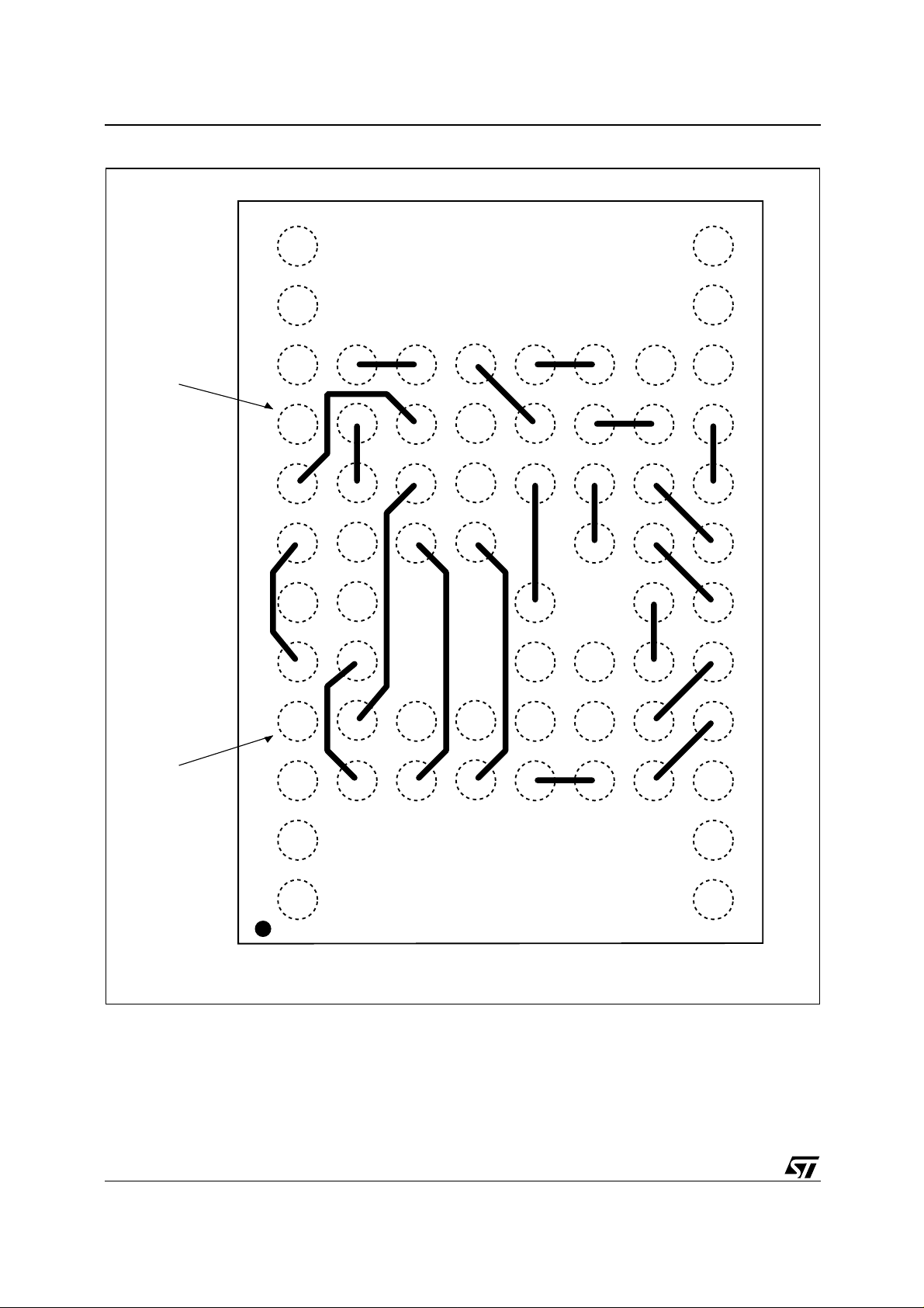
M36W432TG, M36W432BG
Figure 9. Stacked LFBGA66 Daisy Chain - PCB Connections proposal (Top view through package)
#4#3
AI90173
END
POINT
POINT
START
87615
4
32#2
18/66
#1
A
B
C
D
E
F
G
H
M36W432TG, M36W432BG
PART NUMBERING
Table 8. Ordering Information Scheme
Example: M36 W 4 32T G 70 ZA 6 T
Device Type
M36 = MMP (Flash + SRAM)
Operating Voltage
W = V
SRAM Chip Size & Organization
4 = 4 Mbit (256Kb x 16)
Flash Device Size & Organization
32 = 32 Mbit (x16), Boot Block, Flash memory
Array Matrix
T = Top Boot
B = Bottom Boot
SRAM Device
G = 4Mb, 0.16µm, 70ns, 3V
= 2.7V to 3.3V, V
DDF
DDS
= V
= 2.7V to 3.3V
DDQF
Speed
70 = 70ns
85 = 85ns
Package
ZA = LFBGA66: 12 x 8mm, 0.8mm pitch
Temperature Range
1 = 0 to 70°C
6 = –40 to 85°C
Option
T = Tape & Reel packing
Devices are shipped from the factory with the memory content bits erased to ’1’.
Table 9. Daisy Chain Ordering Scheme
Example: M36W432TG -ZA T
Device Type
M36W432TG
Daisy Chain
-ZA = LFBGA66: 12 x 8mm, 0.8mm pitch
Option
T = Tape & Reel Packing
For a list of available options (Speed, Package, etc.) or for further information on any aspect of this device,
please contact the STMicroelectronics Sales Office nearest to you.
19/66

M36W432TG, M36W432BG
FLASH DEVICE
The M36W432TG contains one 32 Mbit Flash
memory. This section describes how to use the
FLASH SUMMARY DESCRIPTION
The Flash Memory is a 32 Mbit (2 Mbit x 16) device
that can be erased electrically at block level and
programmed in-system on a Word-by-Word basis.
These operations can be performed using a single
low voltage (2.7 to 3.6V) supply. V
drive the I/O pin down to 1.65V. An optional 12V
power supply is provided to speed up cus-
V
PPF
tomer programming.
The device features an asymmetrical blocked ar-
chitecture with an array of 71 blocks: 8 Parameter
Blocks of 4 KWords and 63 Main Blocks of 32
KWords. The M36W432TG has the Parameter
Blocks at the top of the memory address space
while the M36W432BG locates the Parameter
Blocks starting from the bottom. The memory
maps are shown in Figure 10, Block Addresses.
The Flash Memory features an instant, individual
block locking scheme that allows any block to be
locked or unlocked with no latency, enabling instant code and data protection. All blocks have
three levels of protection. They can be locked and
locked-down individually preventing any accidental programming or erasure. There is an additional
hardware protection against program and erase.
When V
PPF
≤ V
all blocks are protected
PPLK
DDQF
allows to
Flash device and all signals refer to the Flash device .
against program or erase. All blocks are locked at
Power Up.
Each block can be erased separately. Erase can
be suspended in order to perform either read or
program in any other block and then resumed.
Program can be suspended to read data in any
other block and then resumed. Each block can be
programmed and erased over 100,000 cycles.
The device includes a Protection Register to increase the p rotecti on of a syst em desi gn. The Protection Register is divided into t wo se gments, the
first is a 64 bit area which contains a unique device
number written by ST, while the second is a 128 bit
area, one-time-programmable by the user. The
user programmable segment can be permanent ly
protected. Figure 11, shows the Protection Register Memo ry Map.
Program and Erase command s are written to the
Command Interface of the memory. An on-chip
Program/Erase Controller takes care of the timings necessary for program and erase operations.
The end of a program or erase operation can be
detected and any error conditions identified. The
command set required to control the memory is
consistent with JEDEC standards.
20/66
 Loading...