

SGS Thomson Microelectronics M29W641DL, M29W641DH, M29W641D Datasheet
1/42
PRODUCT PREVIEW
April 2003
This is preliminary information on a new product now in development. Details are subject to change without notice.
M29W641DH, M29W641DL
M29W641DU
64 Mbit (4Mb x16, Uniform Block)
3V Supply F l ash Me m ory
FEATURES SUMMARY
■ SUPPLY VOLTAGE
–V
CC =
2.7V to 3.6V Core Power Supply
–V
CCQ
= 1.8V to 3.6V for Input/Output
–V
PP
=12 V for Fast Program (optional)
■ ACCESS TIME: 70, 90, 100 and 120ns
■ PROGRAMMING TIME
– 10 µs typica l
– Double Word Program option
■ 128 UNIFORM, 32-KWord MEMORY BLOCKS
■ PROGRAM/ERASE CONTROLLER
– Embedded Program and Erase algorithms
■ ERASE SUSPEND and RESUME MODES
– Read and Program another Block during
Erase Suspend
■ UNLOCK BYPASS PROGRAM COMMAND
– Faster Production/Batch Progra mming
■ WRITE PROTECT OPTIONS
– M29W641DH: WP
Pin for Write Protection of
Highest Address Block
– M29W641DL: WP
Pin for Write Protection of
Lowest Address Block
– M29W64 1DU: No Write Protection
■ TEMPORARY BLOCK UNPROTECTION
MODE
■ COMMON FLASH INTERFACE
■ EXTENDED MEMORY BLOCK
– Extra block used as security block or to store
additional information
■ LOW POWER CONSUMPTION
– Standby and Automatic Standby
■ ELECTRONIC SIGNATURE
– Manufacturer Code: 0020h
– Device Code M29W641D: 22C7h
Figure 1. Packages
TSOP48 (N)
12 x 20mm
FBGA
TFBGA63 (ZA)
7 x 11mm

M29W641DH, M29W641DL, M29W641DU
2/42
TABLE OF CONTENTS
SUMMARY DESCRIPTION. . . . . . . . . . . . . . . . . . . . . . . . . . . . . . . . . . . . . . . . . . . . . . . . . . . . . . . . . . . 5
Figure 2. Logic Diagram . . . . . . . . . . . . . . . . . . . . . . . . . . . . . . . . . . . . . . . . . . . . . . . . . . . . . . . . . . 5
Table 1. Signal Names . . . . . . . . . . . . . . . . . . . . . . . . . . . . . . . . . . . . . . . . . . . . . . . . . . . . . . . . . . . 5
Figure 3. TSOP Connections. . . . . . . . . . . . . . . . . . . . . . . . . . . . . . . . . . . . . . . . . . . . . . . . . . . . . . . 6
Figure 4. TFGBA Connections (Top view through package). . . . . . . . . . . . . . . . . . . . . . . . . . . . . . . 7
SIGNAL DESCRIPTIONS . . . . . . . . . . . . . . . . . . . . . . . . . . . . . . . . . . . . . . . . . . . . . . . . . . . . . . . . . . . . 8
Address Inputs (A0-A21). . . . . . . . . . . . . . . . . . . . . . . . . . . . . . . . . . . . . . . . . . . . . . . . . . . . . . . . . . 8
Data Inputs/Outputs (DQ0-DQ7). . . . . . . . . . . . . . . . . . . . . . . . . . . . . . . . . . . . . . . . . . . . . . . . . . . . 8
Data Inputs/Outputs (DQ8-DQ15 ). . . . . . . . . . . . . . . . . . . . . . . . . . . . . . . . . . . . . . . . . . . . . . . . . . . 8
Chip Enable (E). . . . . . . . . . . . . . . . . . . . . . . . . . . . . . . . . . . . . . . . . . . . . . . . . . . . . . . . . . . . . . . . . 8
Output Enable (G). . . . . . . . . . . . . . . . . . . . . . . . . . . . . . . . . . . . . . . . . . . . . . . . . . . . . . . . . . . . . . . 8
Write Enable (W). . . . . . . . . . . . . . . . . . . . . . . . . . . . . . . . . . . . . . . . . . . . . . . . . . . . . . . . . . . . . . . . 8
Write Protect (WP). . . . . . . . . . . . . . . . . . . . . . . . . . . . . . . . . . . . . . . . . . . . . . . . . . . . . . . . . . . . . . . 8
Reset/Block Temporary Unprotect (RP).. . . . . . . . . . . . . . . . . . . . . . . . . . . . . . . . . . . . . . . . . . . . . .8
V
PP
(VPP). . . . . . . . . . . . . . . . . . . . . . . . . . . . . . . . . . . . . . . . . . . . . . . . . . . . . . . . . . . . . . . . . . . . . . 8
V
CC
Supply Voltage (2.7V to 3.6V). . . . . . . . . . . . . . . . . . . . . . . . . . . . . . . . . . . . . . . . . . . . . . . . . . . 8
V
CCQ
Supply Voltage (1.8V to 3.6V). . . . . . . . . . . . . . . . . . . . . . . . . . . . . . . . . . . . . . . . . . . . . . . . . 8
V
SS
Ground. . . . . . . . . . . . . . . . . . . . . . . . . . . . . . . . . . . . . . . . . . . . . . . . . . . . . . . . . . . . . . . . . . . . 9
Table 2. Bus Operations . . . . . . . . . . . . . . . . . . . . . . . . . . . . . . . . . . . . . . . . . . . . . . . . . . . . . . . . . . 9
BUS OPERATIONS. . . . . . . . . . . . . . . . . . . . . . . . . . . . . . . . . . . . . . . . . . . . . . . . . . . . . . . . . . . . . . . . 10
Bus Read. . . . . . . . . . . . . . . . . . . . . . . . . . . . . . . . . . . . . . . . . . . . . . . . . . . . . . . . . . . . . . . . . . . . . 10
Bus Write. . . . . . . . . . . . . . . . . . . . . . . . . . . . . . . . . . . . . . . . . . . . . . . . . . . . . . . . . . . . . . . . . . . . . 10
Output Disable. . . . . . . . . . . . . . . . . . . . . . . . . . . . . . . . . . . . . . . . . . . . . . . . . . . . . . . . . . . . . . . . . 10
Standby. . . . . . . . . . . . . . . . . . . . . . . . . . . . . . . . . . . . . . . . . . . . . . . . . . . . . . . . . . . . . . . . . . . . . . 10
Automatic Standby. . . . . . . . . . . . . . . . . . . . . . . . . . . . . . . . . . . . . . . . . . . . . . . . . . . . . . . . . . . . . . 10
Special Bus Operations . . . . . . . . . . . . . . . . . . . . . . . . . . . . . . . . . . . . . . . . . . . . . . . . . . . . . . . . 1 0
Electronic Signature. . . . . . . . . . . . . . . . . . . . . . . . . . . . . . . . . . . . . . . . . . . . . . . . . . . . . . . . . . . . . 10
Block Protect and Chip Unprotect. . . . . . . . . . . . . . . . . . . . . . . . . . . . . . . . . . . . . . . . . . . . . . . . . . 10
Block Protect and Chip Unprotect. . . . . . . . . . . . . . . . . . . . . . . . . . . . . . . . . . . . . . . . . . . . . . . . . . 10
COMMAND INTERFACE . . . . . . . . . . . . . . . . . . . . . . . . . . . . . . . . . . . . . . . . . . . . . . . . . . . . . . . . . . . 11
Read/Reset Command . . . . . . . . . . . . . . . . . . . . . . . . . . . . . . . . . . . . . . . . . . . . . . . . . . . . . . . . . . 11
Auto Select Command. . . . . . . . . . . . . . . . . . . . . . . . . . . . . . . . . . . . . . . . . . . . . . . . . . . . . . . . . . . 11
Program Command. . . . . . . . . . . . . . . . . . . . . . . . . . . . . . . . . . . . . . . . . . . . . . . . . . . . . . . . . . . . . 11
Unlock Bypass Command. . . . . . . . . . . . . . . . . . . . . . . . . . . . . . . . . . . . . . . . . . . . . . . . . . . . . . . . 12
Unlock Bypass Program Command . . . . . . . . . . . . . . . . . . . . . . . . . . . . . . . . . . . . . . . . . . . . . . . . 12
Unlock Bypass Reset Command. . . . . . . . . . . . . . . . . . . . . . . . . . . . . . . . . . . . . . . . . . . . . . . . . . .12
Chip Erase Command. . . . . . . . . . . . . . . . . . . . . . . . . . . . . . . . . . . . . . . . . . . . . . . . . . . . . . . . . . . 1 2
Block Erase Command . . . . . . . . . . . . . . . . . . . . . . . . . . . . . . . . . . . . . . . . . . . . . . . . . . . . . . . . . . 12
Erase Suspend Comma nd . . . . . . . . . . . . . . . . . . . . . . . . . . . . . . . . . . . . . . . . . . . . . . . . . . . . . . . 13
Erase Resume Command. . . . . . . . . . . . . . . . . . . . . . . . . . . . . . . . . . . . . . . . . . . . . . . . . . . . . . . . 13

3/42
M29W641DH, M29W641DL, M29W641DU
Enter Extended Block Command . . . . . . . . . . . . . . . . . . . . . . . . . . . . . . . . . . . . . . . . . . . . . . . . . .13
Exit Extended Block Command. . . . . . . . . . . . . . . . . . . . . . . . . . . . . . . . . . . . . . . . . . . . . . . . . . . . 13
Table 3. Commands . . . . . . . . . . . . . . . . . . . . . . . . . . . . . . . . . . . . . . . . . . . . . . . . . . . . . . . . . . . . 14
Table 4. Program, Erase Times and Program, Erase E ndurance Cy cles . . . . . . . . . . . . . . . . . . . . 14
STATUS REGISTER. . . . . . . . . . . . . . . . . . . . . . . . . . . . . . . . . . . . . . . . . . . . . . . . . . . . . . . . . . . . . . . 15
Data Polling Bit (DQ7). . . . . . . . . . . . . . . . . . . . . . . . . . . . . . . . . . . . . . . . . . . . . . . . . . . . . . . . . . . 15
Toggle Bit (DQ6).. . . . . . . . . . . . . . . . . . . . . . . . . . . . . . . . . . . . . . . . . . . . . . . . . . . . . . . . . . . . . . . 1 5
Error Bit (DQ5). . . . . . . . . . . . . . . . . . . . . . . . . . . . . . . . . . . . . . . . . . . . . . . . . . . . . . . . . . . . . . . . . 15
Erase Timer Bit (DQ3). . . . . . . . . . . . . . . . . . . . . . . . . . . . . . . . . . . . . . . . . . . . . . . . . . . . . . . . . . . 15
Alternative Toggle Bit (DQ2).. . . . . . . . . . . . . . . . . . . . . . . . . . . . . . . . . . . . . . . . . . . . . . . . . . . . . . 1 5
Table 5. Status Register Bits. . . . . . . . . . . . . . . . . . . . . . . . . . . . . . . . . . . . . . . . . . . . . . . . . . . . . . 16
Figure 5. Data Polling Flowchart . . . . . . . . . . . . . . . . . . . . . . . . . . . . . . . . . . . . . . . . . . . . . . . . . . . 17
Figure 6. Data Toggle Flowchart. . . . . . . . . . . . . . . . . . . . . . . . . . . . . . . . . . . . . . . . . . . . . . . . . . . 17
MAXIMUM RATING. . . . . . . . . . . . . . . . . . . . . . . . . . . . . . . . . . . . . . . . . . . . . . . . . . . . . . . . . . . . . . . . 18
Table 6. Absolute Maximum Ratings . . . . . . . . . . . . . . . . . . . . . . . . . . . . . . . . . . . . . . . . . . . . . . . .18
DC and AC PARAMETERS . . . . . . . . . . . . . . . . . . . . . . . . . . . . . . . . . . . . . . . . . . . . . . . . . . . . . . . . . 1 9
Table 7. Operating and AC Measurement Condition s. . . . . . . . . . . . . . . . . . . . . . . . . . . . . . . . . . . 19
Figure 7. AC Measurement I/O Waveform . . . . . . . . . . . . . . . . . . . . . . . . . . . . . . . . . . . . . . . . . . . 19
Figure 8. AC Measurement Load Circuit . . . . . . . . . . . . . . . . . . . . . . . . . . . . . . . . . . . . . . . . . . . . . 19
Table 8. Device Capacitance. . . . . . . . . . . . . . . . . . . . . . . . . . . . . . . . . . . . . . . . . . . . . . . . . . . . . . 1 9
Table 9. DC Characteristics. . . . . . . . . . . . . . . . . . . . . . . . . . . . . . . . . . . . . . . . . . . . . . . . . . . . . . . 2 0
Figure 9. Read Mode AC Waveforms . . . . . . . . . . . . . . . . . . . . . . . . . . . . . . . . . . . . . . . . . . . . . . . 21
Table 10. Read AC Characteristics . . . . . . . . . . . . . . . . . . . . . . . . . . . . . . . . . . . . . . . . . . . . . . . . . 21
Figure 10. Write AC Waveforms, Write Enable Controlled . . . . . . . . . . . . . . . . . . . . . . . . . . . . . . . 22
Table 11. Write AC Characteristics, Write Enable Controlled . . . . . . . . . . . . . . . . . . . . . . . . . . . . . 22
Figure 11. Write AC Waveforms, Chip Enable Controlled. . . . . . . . . . . . . . . . . . . . . . . . . . . . . . . . 23
Table 12. Write AC Characteristics, Chip Enable Controlled . . . . . . . . . . . . . . . . . . . . . . . . . . . . . 23
Figure 12. Reset/Block Temporary Unprotect AC Waveforms . . . . . . . . . . . . . . . . . . . . . . . . . . . . 24
Table 13. Reset/Block Temporary Unprotect AC Characteristics . . . . . . . . . . . . . . . . . . . . . . . . . . 24
Figure 13. Accelerated Program Timing Waveforms. . . . . . . . . . . . . . . . . . . . . . . . . . . . . . . . . . . . 24
PACKAGE MECHANICAL . . . . . . . . . . . . . . . . . . . . . . . . . . . . . . . . . . . . . . . . . . . . . . . . . . . . . . . . . . 25
Figure 14. TSOP48 – 48 lead Plastic Thin Small Outline, 12 x 20mm, Package Outline . . . . . . . . 25
Table 14. TSOP48 – 48 lead Plastic Thin Small Outline, 12 x 20mm, Package Mechanical Data . 25
Figure 15. TFBGA63 - 7x11mm, 6x8 active ball array, 0.8mm pitch, Bottom view packag e outline26
Table 15. TFBGA63 - 7x11mm, 6x8 active ball array, 0.8mm pitch, Package Mech anical Data . . 26
PART NUMBERING . . . . . . . . . . . . . . . . . . . . . . . . . . . . . . . . . . . . . . . . . . . . . . . . . . . . . . . . . . . . . . . 27
Table 16. Ordering Information Scheme . . . . . . . . . . . . . . . . . . . . . . . . . . . . . . . . . . . . . . . . . . . . . 27
APPENDIX A. BLOCK ADDRESSES. . . . . . . . . . . . . . . . . . . . . . . . . . . . . . . . . . . . . . . . . . . . . . . . . . 28
Table 17. Block Addresses . . . . . . . . . . . . . . . . . . . . . . . . . . . . . . . . . . . . . . . . . . . . . . . . . . . . . . . 28

M29W641DH, M29W641DL, M29W641DU
4/42
APPENDIX B. COMMON FLASH INTERFACE (CFI) . . . . . . . . . . . . . . . . . . . . . . . . . . . . . . . . . . . . . 32
Table 18. Query Structure Overview . . . . . . . . . . . . . . . . . . . . . . . . . . . . . . . . . . . . . . . . . . . . . . . .32
Table 19. CFI Query Identification String . . . . . . . . . . . . . . . . . . . . . . . . . . . . . . . . . . . . . . . . . . . .32
Table 20. CFI Query System Interface Information. . . . . . . . . . . . . . . . . . . . . . . . . . . . . . . . . . . . . 33
Table 21. Device Geometry Definition. . . . . . . . . . . . . . . . . . . . . . . . . . . . . . . . . . . . . . . . . . . . . . .33
Table 22. Primary Algorithm-Spe cific Extended Query Table . . . . . . . . . . . . . . . . . . . . . . . . . . . . . 34
Table 23. Security Code Area . . . . . . . . . . . . . . . . . . . . . . . . . . . . . . . . . . . . . . . . . . . . . . . . . . . . . 3 4
APPENDIX C. EXTENDED MEMORY BLOCK . . . . . . . . . . . . . . . . . . . . . . . . . . . . . . . . . . . . . . . . . . 35
Factory Locked Extended Block . . . . . . . . . . . . . . . . . . . . . . . . . . . . . . . . . . . . . . . . . . . . . . . . . 35
Customer Lockable Extended Block. . . . . . . . . . . . . . . . . . . . . . . . . . . . . . . . . . . . . . . . . . . . . . 35
Table 24. Extended Block Address and Data . . . . . . . . . . . . . . . . . . . . . . . . . . . . . . . . . . . . . . . . . 35
APPENDIX D. BLOCK PROTECTION . . . . . . . . . . . . . . . . . . . . . . . . . . . . . . . . . . . . . . . . . . . . . . . . . 36
Programmer Technique . . . . . . . . . . . . . . . . . . . . . . . . . . . . . . . . . . . . . . . . . . . . . . . . . . . . . . . . 36
In-System Technique . . . . . . . . . . . . . . . . . . . . . . . . . . . . . . . . . . . . . . . . . . . . . . . . . . . . . . . . . . 36
Table 25. Programmer Technique Bus Operations . . . . . . . . . . . . . . . . . . . . . . . . . . . . . . . . . . . . . 36
Figure 16. Programmer Equipment Group Protect Flowchart. . . . . . . . . . . . . . . . . . . . . . . . . . . . . 37
Figure 17. Programmer Equipment Chip Unprotect Flowchart . . . . . . . . . . . . . . . . . . . . . . . . . . . . 38
Figure 18. In-System Equipment Group Protect Flowchart. . . . . . . . . . . . . . . . . . . . . . . . . . . . . . . 39
Figure 19. In-System Equipment Chip Unprotect Flowchart . . . . . . . . . . . . . . . . . . . . . . . . . . . . . . 40
REVISION HISTORY. . . . . . . . . . . . . . . . . . . . . . . . . . . . . . . . . . . . . . . . . . . . . . . . . . . . . . . . . . . . . . . 41
Table 26. Document Revision History. . . . . . . . . . . . . . . . . . . . . . . . . . . . . . . . . . . . . . . . . . . . . . .41
5/42
M29W641DH, M29W641DL, M29W641DU
SUMMARY DESCRIPTION
The M29W641D is a 64 M bit (4Mb x16 ) non-v olatile memory that can be read, erased and reprogrammed. These operations can be performed
using a single, low voltage, 2.7V to 3.6V V
CC
sup-
ply for the circuitry and a 1.8V to 3.6V V
CCQ
supply
for the Input/Output pins. An optional 12 V V
PP
power supply is provided to speed up customer
programming.
On power-up the memory defaults to its Read
mode where it can be read in the same way as a
ROM or EPROM.
The highest address blo ck of t he M 29W6 41DH or
the lowest address block of the M29W641 DL can
be protected from accidental programming or erasure using the WP
pin (if WP = VIL). The
M29W641DU doe s not feature the WP
pin.
Each block can be erase d independently so it is
possible to preserve valid data while old data is
erased. The blocks can be protected to prevent
accidental Program or Erase commands from
modifying the me mory. Program an d Erase commands are written to the Command Interface of
the memory. An on-chip Program/Erase Controller
simplifies the process of programming or e rasing
the memory by taking care of all of the special operations that are required to update the memory
contents. The end of a program or erase operation
can be detected and any error conditions identified. The command set required to control the
memory is consistent with JEDEC standards.
The M29W641D has an extra block, the Extended
Block, (of 32 KWords) that can be accessed using
a dedicated command. The Extended Block can
be protected and s o is useful for storing security
information. However the prot ection i s not reversible, once protected the protection cannot be undone.
Chip Enable, Output Enable and Write Enable signals control the bus operation of the memory.
They allow simple connection to most microprocessors, often without additional logic.
The memory is offered in a 48-pin TSOP package
(M29W641DL and M29W641DH) or i n a 63-ball TFBGA pack age (M29W64 1DU). All de vices a re del ivered with all the bits e ras ed (set to 1).
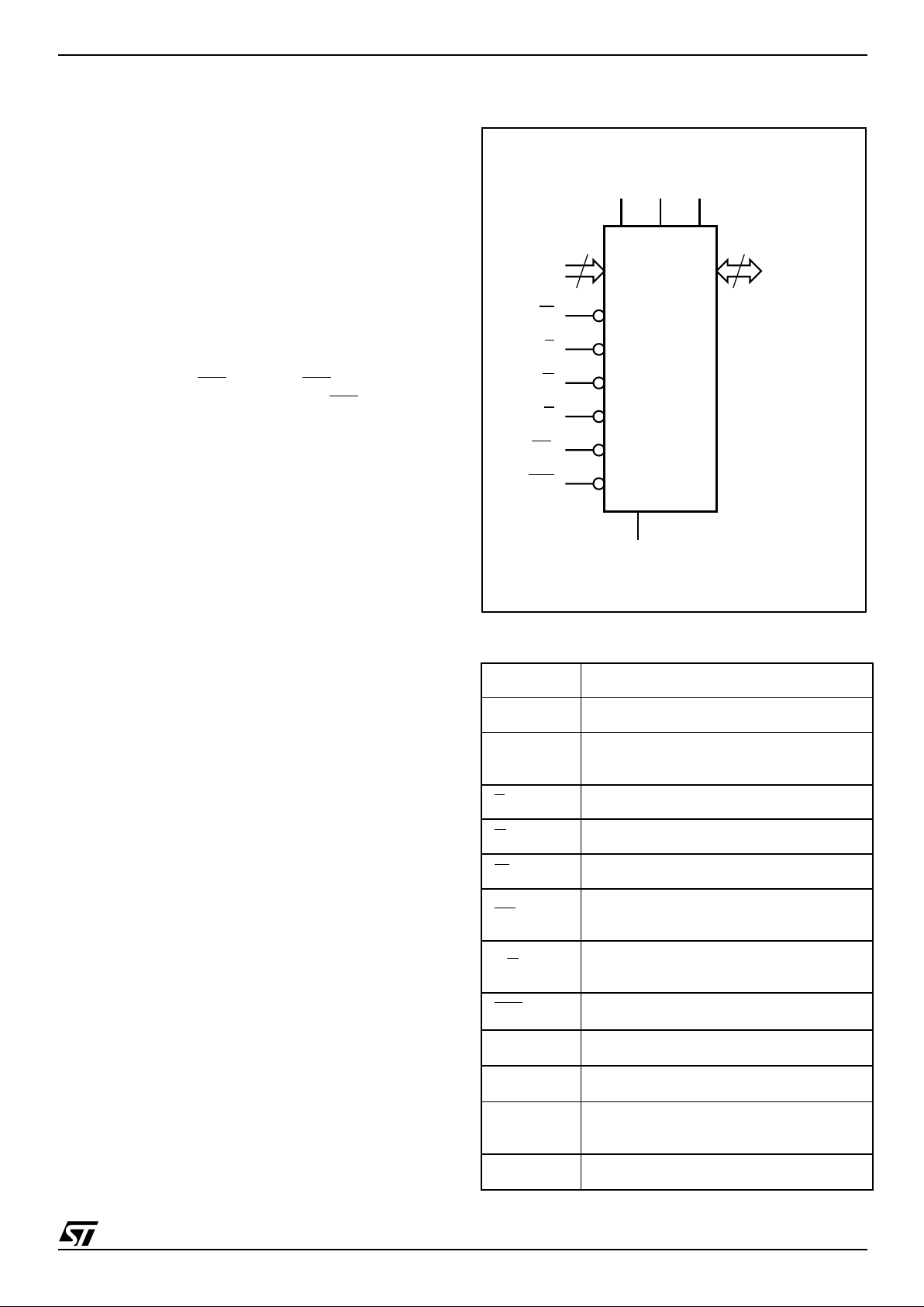
Figure 2. L o gi c D iagram
Table 1. Signal Names
A0-A21 Address Inputs
DQ0-DQ7 Data Inputs/Outputs
DQ8-
DQ15
Data Inputs/Outputs
E
Chip Enable
G
Output Enable
W
Write Enable
RP
Reset/Block Temporary Unprotect
(M29W641DH and M29W641DL only)
RB
Ready/Busy Output (M29W641DU
only)
WP
Write Protect
V
CC
Supply Voltage
V
CCQ
Supply Voltage for Input/Output
V
PP
Supply Voltage for Fast Program
(optional)
V
SS
Ground
AI06697b
22
A0-A21
W
DQ0-DQ15
V
CC
M29W641D
E
V
SS
16
G
RP
V
PP
WP
V
CCQ
RB
M29W641DH, M29W641DL, M29W641DU
6/42
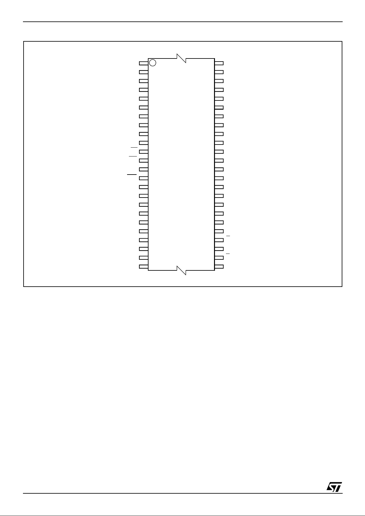
Figure 3. TSOP C on ne cti ons
DQ3
DQ9
DQ2
A6
DQ0
W
A3
A19
DQ6
A8
A9
DQ13
A17
A10 DQ14
A2
DQ12
DQ10
DQ15
V
CC
DQ4
DQ5
A7
DQ7
WP
V
PP
M29W641D
12
1
13
24 25
36
37
48
DQ8
A20
A21
A1
A18
A4
A5
DQ1
DQ11
G
A12
A13
A16
A11
V
CCQ
A15
A14
V
SS
E
A0
RP
V
SS
AI06698
7/42
M29W641DH, M29W641DL, M29W641DU
Figure 4. TFGBA Connections (Top view through package)
Note: 1. Bal l s are shorte d to gether via the substrat e but not connec te d to the die.
654321
V
SS
A15
A14
A12
A13
DQ3
DQ11
DQ10
A18
V
PP
RB
DQ1
DQ9
DQ8
DQ0
A6
A17
A7
G
E
A0
A4
A3
DQ2
DQ6
DQ13
DQ14
A10
A8
A9
DQ4
V
CC
DQ12
DQ5
A19
A21
RP
W
A11
DQ7
A1
A2
V
SS
A5 A20
A16
C
B
A
E
D
F
G
H
DQ15
NC
(1)
NC
(1)
NC
(1)
NC
(1)
NC
(1)
NC
(1)
NC
(1)
NC
(1)
NC
(1)
NC
(1)
NC
(1)
J
K
L
M
87
NC
(1)
NC
(1)
NC
(1)
NC
(1)
AI06879
V
CCQ

M29W641DH, M29W641DL, M29W641DU
8/42
SIGNAL DESCRIPTIONS
See Figure 2, Logic Diagram, and T able 1, Signal
Names, for a brief overview of the signals connected to this device.
Address Inputs (A0-A21). The Address Inputs
select the cell s in the memory arra y to access during Bus Read operations. During Bus Write operations they control the commands sent to the
Command Interface of the Program/Erase Controller.
Data Inputs/Outputs (DQ0-DQ7). The Data I/O
outputs the data stored at the selected address
during a Bus Read operation. During Bus Write
operations they represent the commands sent to
the Command Interface of the Program/Erase
Controller.
Data Inputs/Outputs (DQ8-DQ15). The Data I/O
outputs the data stored at the selected address
during a Bus Read operation. During Bus Write
operations the Command Register does not use
these bits. When reading the Status Register
these bits should be ignored.
Chip Enable (E
). The Chip Enable, E, activates
the memory, allowing Bus Read and Bus Write operations to be performed. When Chip Enable is
High, V
IH
, all other pins are ignored.
Output Enable (G
). The Output Enable, G, con-
trols the Bus Read operation of the memory.
Write Enable (W
). The Write Enable, W, controls
the Bus Write operation of the memory’s Command Interface.
Write Protect (W
P). The Write Protect pin is
available in the M29W641DH and M29W641DL
only. I t provid es a hard war e metho d of pro tecting
the highest address block for the M29W641DH
and the lowest address block for the
M29W 641DL. The Write Protect pin must not be
left floating or unconnected.
When Write Protect is Low, V
IL
, the memory protects either the highest or lowest address block;
Program and Erase operations in this block are ignored while Write Protect is Low.
When Write P rotect
is High, VIH, the memory reverts to the previous protection status for this
block. Program and Erase operations can now
modify the data in this block unless the block is
protected using Block Protection.
Ready/Busy Output (RB
). The Ready/Busy pin
is an open-drain output that can be used to identify
when the device is performing a Program or Erase
operation. During Program or Erase operations
Ready/Busy is Low, V
OL
. Ready/Busy is high-impedance during Read mode, Auto Select mode
and Erase Suspend mode.
After a Hardware Reset, Bus Read and Bus Write
operations cannot begin until Ready/Busy be-
comes high-impedanc e. See Tabl e 13 a nd Fi gure
12, Reset/Block Temporary Unprotect AC Characteristics.
The use of an open-drain output allows the Ready/
Busy pins from several memories to be connected
to a single pull-up resistor. A Low will then indicate
that one, or more, of the memories is busy.
Reset/Block Temporary Unprotect (RP
). The
Reset/Block Temporary Unprotect pin can be
used to apply a Hardware Reset to the memory or
to temporarily unprotect all Blocks that have been
protected.
Note that if Write Protect
(WP) is at VIL, then one
of the two ou termost blocks will remain p rotected
even if RP is at V
ID
.
A Hardware Reset is achieved by holding Reset/
Block Temporary Unprotect Low, V
IL
, for at least
t
PLPX
. After Reset/Block Temporary Unprotect
goes High, V
IH
, the memory will be ready for Bus
Read and Bus Write operations after t
PHEL
or
t
RHEL
, whichever occurs last. See Table 13 and
Figure 12, Reset/Block T emporary Unprotect AC
Characteristics, for more details.
Holding RP
at VID will temporarily unprotect the
protected Blocks in the memory. Program and
Erase operations on all blocks will be possible.
The transition from V
IH
to VID must be slower than
t
PHPHH
.
V
PP
(VPP). When the VPP pin is raised to V
PPH
the memory automatically enters the Unlock Bypass mode. When the pin is returned to V
IH
or V
IL
normal operation resumes. During Unlock Bypass
Program operations the memory draws I
PP
from
the pin to supply the programming circuits. See the
description of the Unlock Bypas s c ommand in the
Command Interface section. The transitions from
V
IH
to VPP and from VPP to VIH must be slower
than t
VHVPP
, see Figure 13.
Never raise the pin to V
PP
from any mode except
Read mode, otherwise the memory may be left in
an indeterminate state.
V
CC
Supply Voltage (2.7V to 3.6V). VCC pro-
vides the power supply for all operations (Read,
Program and Erase).
The Command Interface is disabled when the V
CC
Supply Voltage is less than the L ockout Voltage,
V
LKO
. This prevents Bus Write operations from accidentally damaging the data during power up,
power down and power surges. If the Program/
Erase Controller is programming or erasing during
this time then the operation aborts and the memory contents being altered will be invalid.
V
CCQ
Supply Voltage (1.8V to 3.6V). V
CCQ
provides the power supply to the I/O pins and enables
all Outputs to be powered i ndependently of V
CC
.
9/42
M29W641DH, M29W641DL, M29W641DU
V
CCQ
can be tied to VCC or can use a separate
supply.
V
SS
Ground. VSS is the reference for all voltage
measurements. The device f eatures two V
SS
pins
which must be both connected to the system
ground.
Note: Each device in a system should have
V
CC, VCCQ
and VPP decoupled from V
SS
with a
0.1µF ceramic capacitor close to the pin for
current surge protection (high frequency, inherently low inductan ce capacitors should b e
as close as possible to the device). See Figure
8, AC Measurement Load Circuit. The PCB
trace widths should be sufficient to carry the
required V
PP
program and erase currents. See
Table 9, DC Characteristics.
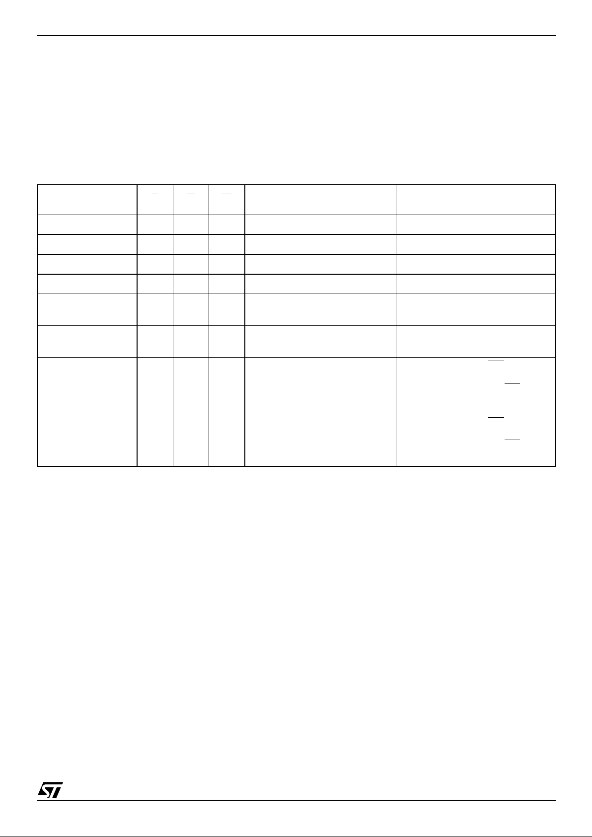
Table 2. Bus Operations
Note: X = VIL or VIH.
Operation E G W
Address Inputs
A0-A21
Data Inputs/Outputs
DQ15-DQ0
Bus Read
V
IL
V
IL
V
IH
Cell Address Data Output
Bus Write
V
IL
V
IH
V
IL
Command Address Data Input
Output Disable X
V
IH
V
IH
X Hi-Z
Standby
V
IH
X X X Hi-Z
Read Manufacturer
Code
V
IL
V
IL
V
IH
A0 = VIL, A1 = VIL, A9 = VID,
Others V
IL
or V
IH
0020h
Read Device Code
V
IL
V
IL
V
IH
A0 = VIH, A1 = VIL, A9 = VID,
Others V
IL
or V
IH
22C7h
Extended Memory
Block Verify Code
V
IL
V
IL
V
IH
A0 = VIH, A1 = VIH, A6 = VIL,
A9 = V
ID
, Others VIL or V
IH
98h (factory locked, WP protects
highest address block)
18h (not factory locked, WP
protects highest address
block)
88h (factory locked, WP
protects
lowest block)
08h (not factory locked, WP
protects lowest block)

M29W641DH, M29W641DL, M29W641DU
10/42
BUS OPERATIONS
There are five standard bus operations that control
the device. These are B us Read, Bus Wri te, Output Disable, Standby and Automatic Standby. See
Table 2, Bus Operations, for a summary. Typically
glitches of less t han 5ns on Chip E nable o r Write
Enable are ignored by the memory and do not a ffect bus operations.
Bus Read. Bus Read operations read from the
memory cells, or specific registers in the Command Interface. A valid Bus Read operation involves setting the desired address on the Address
Inputs, applying a Low signal, V
IL
, to Chip Enable
and Output Enable and keeping Write Enable
High, V
IH
. The Data Inputs/Outputs will outp ut the
value, see Figure 9 , Read Mode AC Waveforms,
and Table 10, Read AC Characteristics, for details
of when the output becomes valid.
Bus Write. Bus Write operations write to the
Command Interface. A valid Bus Write operation
begins by setting th e desired address o n the Address Inputs. The Address Input s are latched by
the Command Interface on the falling edge of Chip
Enable or Write Enable, whichever occurs last.
The Data Inputs/Outputs a re latc hed by the Com mand Interface on the rising edge of Chip Enable
or Write Enable, whichever occurs first. Output Enable must remain High, V
IH
, during the whole Bus
Write operation. See Figure 10 and Figure 11,
Write AC Waveforms, and Table 11 and Table 12,
Write AC Characteristics, for details of the timing
requirements.
Output Disable. T he Data Inputs/Outputs are in
the high impedanc e state when Out put Enable is
High, V
IH
.
Standby. When Chip Enable is High, V
IH
, the
memory enters Standby mode and the Data Inputs/Outputs pins are placed in the high-impedance state. To reduce t he Supply Current to the
Standby Supply Current, I
CC2
, Chip Enable should
be held within V
CC
± 0.2V. For the Standby current
level see Table 9, DC Characteristics.
During program or erase operations the memory
will continue to use the Program/Erase Supply
Current, I
CC3
, for Program or Erase operations un-
til the operation completes.
Automatic Standby. If CMOS levels (V
CC
± 0.2V)
are used to drive the bus and the bus is inactive for
300ns or more the memory enters Automatic
Standby where the internal Supply Current is reduced to the Standby Supply Current, I
CC2
. The
Data Inputs/Outputs will still output data if a Bus
Read operation is in progress.
Special Bus Operations
Additional bus operations can be performed to
read the Electronic Signature and also to apply
and remove Block Protection. These bus operations are intended for use by programming equipment and are not usually used in applications.
They require V
ID
to be applied to some pins.
Electronic Signature. The memory has two
codes, the manufacturer code and the device
code, that can be read to identify the memory.
These codes can be read by app lying the signals
listed in Table 2, Bus Operations.
Block Protect and Chip Unprotect.
Groups of
blocks can be protected against accidental Program or Erase. The whole chip can be unprotected
to allow the data inside the blocks to be changed.
Write Protect
(WP) can be used to protect one of
the outermost blocks. When Write Protect
(WP) is
at V
IL
one of the two outer m os t blocks i s prot e cted and r emai ns prot ect ed r eg ardle s s of the Bl ock
Protection Status or the Reset/Block Temporary
Unprotect pin stat us. For th e M29W641D H, it is
the highest addressed block that can be protected. For the M29 W641DL, i t i s the lowest.
Block Protect and Chip Un protect operations are
described in Appendix D.

11/42
M29W641DH, M29W641DL, M29W641DU
COMMAND INTERFACE
All Bus Write operations to the memory are in terpreted by the Command Interface. Commands
consist of one or more sequential Bus Write operations. Failure to observe a valid sequence of Bus
Write operations will result in the memory returning to Read mode. The long command sequences
are imposed to maximize data security.
See Table 3 for a summary of the commands.
Read/Reset Command
The Read/Reset command returns the memory to
its Read mode where it behaves like a ROM or
EPROM. It also resets the errors in the Status
Register. Either one or three Bus Write operations
can be used to issue the Read/Reset command.
The Read/Reset command can be issued, between Bus Write cycles before the start of a program or erase operation, to return the device to
read mode. If the Read/Reset command is issued
during the timeout of a Block erase operation then
the memory will take up to 10µs to abort. During
the abort period no valid data can be read from the
memory. The Read/Reset command will not abort
an Erase operation when issued while in Erase
Suspend.
Auto Select Command
The Auto Select command is used to read the
Manufacturer Code, the Device Code, the Block
Protection Status and the Extended Memory Block
Verify Code. Three consecut ive Bus W rite operations are required to issue the Auto Select command. Once the Auto Select command is issued
the memory remains in Auto S elect mode until a
Read/Reset command is issued. Read CFI Query
and Read/Reset com ma nds are accepted in Aut o
Select mode, all other commands are ignored.
In Auto Select mode the Manuf acturer Code can
be read using a Bus Read operation with A0 = V
IL
and A1 = VIL. The other address bits may be set to
either V
IL
or VIH. The Manufacturer Co de for ST-
Microelectronics is 0020h.
The Device Code can be read using a Bus Read
operation with A0 = V
IH
and A1 = VIL. The other
address bits may be set to e ither V
IL
or VIH. The
Device Code for the M29W641D is 22C7h.
The B l ock Protecti on Sta tus of each block can be
read using a Bus Read operation with A0 = V
IL
,
A1 = V
IH
, and A 12-A21 sp ecifyin g t h e addres s of
the b lock. T he oth er addr ess bi ts may b e set t o either V
IL
or VIH. If th e addr ess ed bloc k is p rot ecte d
then 01h is output on Data Inputs/Outputs DQ0DQ7, otherwise 00h is output.
Read CFI Query Command
The Read CFI Query Command is used to read
data from the Common Flash Interface (CFI)
Memory Area. This command is valid when the de-
vice is in the Read Array mode, or when the device
is in Autos ele c t e d mo de.
One Bus Write cycle is required to issue the Read
CFI Query Command. Once the command is issued subsequent Bus Read ope rations read from
the Common Flash Interface Memory Area.
The Read/Reset comm and must be issued to return the device to the previous mode (the Read Array mode or Autoselected mode). A second Read/
Reset command would be needed if the device is
to be put in the Read Array mode from Autoselected mode.
See Appendix B, Ta ble 18 to Table 23 for details
on the information contained in the Common Flash
Interface (CFI) memory area.
Program Command
The Program command can be used to program a
value to one address in the memory array at a
time. The command requires four Bus Write operations, the final write operation latches the address and data, and starts the Program/Erase
Controller.
If the address falls in a protected block then the
Program command is ignored, the data remains
unchanged. The Status Register is never read and
no error condition is given.
During the program operat ion the me mory will ignore all commands. I t is not possible to issue any
command to abort or pause the operation. Typical
program times are given in Table 4. Bus Read operations during the program o peration will output
the Status Register on the Data Inputs/Outputs.
See the section on t he Status Register for more
details.
After the program operation has completed the
memory will return to the Read mode, unless an
error has occurred. When an error occurs the
memory will continue to output the Status Register. A Read/Reset command must be issued to reset the error condition and return to Read mode.
Note that the Program command cannot change a
bit set at ’0’ back to ’1’. One of the Erase Commands must be used to set all the bits in a block or
in the whole memory from ’0’ to ’1’.
Fast Program Commands
There is a Fast Program command available to improve the programming throughput, by writing several adjacent words or bytes in parallel: the Double
Word Program command.
Double Word Program Command. The Doub l e
Word Program comm and is used to write a page
of two adjacent words in paral lel. The two words
must differ only for the address A0.
Three bus write cycles are necessary to issue the
Double Word Program command.

M29W641DH, M29W641DL, M29W641DU
12/42
■ The first bus cycle sets up the Double Word
Program Command.
■ The second bus cycle latches the Address and
the Data of the first word to be written.
■ The third bus cycle latches the Address and the
Data of the second word to be written and starts
the Program/Erase Controller.
Only one bank can be programmed at any one
time. The other b ank must be in Read mode or
Erase Suspend.
Programming should not be attempted when V
PP
is not at V
PPH
.
After programming has started, Bus Read operations in the Bank being programmed output the
Status Register content, while Bus Read operations to the oth er Bank o utput the c ontents of t he
memory a r ra y.
After the program operation has completed the
memory will return to the Read mode, unless an
error has occurred. When an error occurs Bus
Read operations to the Bank where the command
was issued will continue to output the Status Register. A Read/Reset command must be issued to
reset the error condition and return to Read mode.
Note that the Fast Program commands cannot
change a bit set at ’0’ back to ’1’. One of the Erase
Commands must be used to set all the bits in a
block or in the whole memory from ’0’ to ’1’.
Typical Program time s are given in Tab le 4, Program, Erase Times and Program, Erase Endurance Cycles.
Unlock Bypass Command
The Unlock Bypass command is used in conjunction with the Unlock Bypass Program command to
program the memory faster than with the standard
program commands. Whe n the cycle time to the
device is long (as with some EPROM programmers) considerable time saving can be made by
using these commands. Three Bus Write operations are required to issue the Unlock Bypass
command.
Once the Unlock By pass command has been issued the memory enters Unlock Bypass mode.
When in this mode the memory can be read as if
in Read mode.
When V
PPH
is applied to the VPP pin the memory
automatically enters the Unlock Bypass mode and
the Unlock Bypass Program command can be issued immediately.
Unlock Bypass Program Command
The Unlock Bypass Program command can be
used to program one address in the memory array
at a time. The command requires t wo Bus Write
operations, the final write operation latches the ad-
dress and data, and starts the Program/Erase
Controller.
A Program operation initiated by issuing the Unlock Bypass Program command is identical to a
Program operation initiated by issuing the Program command. It cannot be aborted and a B us
Read operation will output the Status Register.
See the Program Comma nd paragraph for further
details.
Unlock Bypass Reset Command
The Unlock Bypass R eset com m and c an b e us ed
to return to Read/Reset mode from Unlock Bypass
Mode. Two Bus Write operations are required to
issue the Unlock Bypass Reset command. Read/
Reset command does not exit from Unlock Bypass
Mode.
Chip Erase Command
The Chip Erase command can be used to erase
the entire chip. Six Bus Write operations a re required to issue the Chip Erase Command and start
the Program/Erase Controller.
If any blocks are protected then these are ignored
and all the other blocks are erased. If all of the
blocks are protected the Chip Erase operat i on appears to start but will terminate within about 100µs,
leaving the data unchanged. No error condition is
given when protected blocks are ignored.
During the erase operation the memory will ignore
all commands, including the Erase Suspen d command. It is not possible t o issue any comm and to
abort the operation. Typical chip erase t imes are
given in Table 4. All Bus Read operations during
the Chip Erase operation will output the Status
Register on the Data Inputs/Outputs. See the section on the Status Register for more details.
After the Chip Erase operation has com pleted the
memory will return to the Read Mode, unless an
error has occurred. When an error occurs the
memory will continue to output the Status Register. A Read/Reset command must be issued to reset the error condition and return to Read Mode.
The Chip Erase Command sets all of the bits in unprotected blocks of the memory to ’1’. All previous
data is lost.
Block Erase Command
The Block Erase c ommand can be used to erase
a list of one or more blocks. Six Bus Write operations are required to select the first block i n the list.
Each additional block in the list can be selected by
repeating the sixth Bus Write operat ion using the
address of the additional block. The Block Erase
operation starts the Program/Erase Controller
about 50µs after the last Bus Write operation.
Once the P rogram /Erase Controller starts it is not
possible to select any more blocks. Each additional block must therefore be selected within 50µ s of

13/42
M29W641DH, M29W641DL, M29W641DU
the lowest address block. The 50µs time r restarts
when an additional block is selected. The Status
Register can be read after the sixth Bus Write operation. See the Status Register section for details
on how to identify if the P rogram /Erase Cont roller
has started the Block Erase operation.
If any selected blocks are protected then these are
ignored and all the other selected blocks are
erased. If all of the selected blocks are p rotected
the Block Erase operation appears to start but will
terminate within about 100µs, leaving the data unchanged. No error condition is given when protected blocks are ignored.
During the Block Erase operation th e memory wi ll
ignore all commands except the Erase Suspend
command. Typical block era se t imes a re given in
Table 4. All Bus Read operations during the Block
Erase operation w ill ou t pu t the S t a tus R eg i st er on
the Data Inputs/Outputs. See the section on the
Status Register for more details.
After the Block Erase operation has completed the
memory will return to the Read Mode, unless an
error has occurred. When an error occurs the
memory will continue to output the Status Register. A Read/Reset command must be issued to reset the error condition and return to Read mode.
The Block Erase Command sets all of the bits in
the unprotected selected blocks to ’1’. All previous
data in the selected blocks is lost.
Erase Suspend Command
The Erase Suspend Command may be used to
temporarily suspend a Block Erase o peration and
return the memory to Read mode. The com mand
requires one Bus Write operation.
The Program/Erase Controlle r will suspend within
the Erase Suspend Latency time of the Erase Suspend Command being issued. Once the Program/
Erase Controller has stopped the mem ory will be
set to Read mode and t he E rase wi ll be suspended. If the Erase Suspend c ommand is issued during the period when the memory is waiting for an
additional block (before the Program/E rase Controller starts) then the Erase is suspended immediately and will start immediately when the Erase
Resume Command is issued. It is not poss ible to
select any further blocks to erase after the Erase
Resume.
During Erase Suspend it is possible to Read and
Program cells in blocks that are not being erased;
both Read and Program operations behave as
normal on these blocks. If any attempt is made to
program in a protected block or in the suspen ded
block then the Program co mmand is ignored and
the data remains unchanged. The Status Register
is not read and no error condi tion is given. Reading from blocks that are being erased will output
the Status Register.
It is also possible to issue the Auto Select, Read
CFI Query and Unlock Bypass commands du ring
an Erase Suspend. The Read/Reset command
must be issued to return the device to Read Array
mode before the Resume command will be accepted.
Erase Resume Command
The Erase Resume command must be used to restart the Program/Erase Controller after an Erase
Suspend. The device must be in Read Array mode
before the Resume command will be accepted. An
erase can be suspended and resumed mo re than
once.
Enter Extended Block Command
The device has an extra 32 KWord block (Extended Block) that can only be accessed using the Enter Extended Block command. Three Bus write
cycles are required to issue the Extended Block
command. Once the command has been issued
the device enters Extende d Block mo de where a ll
Bus Read or Write operations to the Boot Block
addresses access the Extended Block. The Extended Block (with the same address as the Boot
Blocks) cannot be erased, and c an be treated as
one-time programmable (OTP) memory. In Extended Block mode the Boot Blocks are not accessible.
To exit from the Extended Block mode the Exit Extended Block command must be issued.
The Extended Block can be protected, however
once protected the protection cannot be undone.
Exit Exte nded Block Com m and
The Exit Extended Block command is used to exit
from the Extended Block mod e and return t he device to Read mode. Four Bus Write operations are
required to issue the command.
Block Protect and Chip Unprotect Commands
Groups of blocks can be protected against acci-
dental Program or Erase. The whole chip can be
unprotected to allow the dat a inside the blocks to
be changed.
Block Protect and Chip Un protect operations are
described in Appendix D.
 Loading...