

64 Mbit (8Mb x8 or 4Mb x16, Boot Block)
FEATURES SUMMARY
■ SUPPLY VOLTAGE
–V
–V
■ ACCESS TIME: 70, 90 ns
■ PROGRAMMING TIME
– 10 µs per Byte/Word typical
– Double Word Programming Option
■ 135 MEMORY BLOCKS
– 1 Boot Block and 7 Parameter Blocks,
– 127 Main Blocks, 64 KBytes each
■ PROGRAM/E RA SE CONTROLLER
– Embedded Byte/Word Program algorithms
■ ERASE SUSPEND and RESUME MODES
– Read and Program another Block during
■ UNLOCK BYPASS PROGRAM COMMAND
– Faster Production/Batch Programm ing
■ V
PP
PROTECT
■ TEMPORARY BLOCK UNPROTECTION
MODE
■ COMMON FLASH INTERFACE
– 64-bit Security Code
■ EXTENDED MEMORY BLOCK
– Extra block used as security block or to store
■ LOW POWER CONSUMPTION
– Standby and Automatic Standby
■ 100,000 PROGRAM/ER ASE CYCL ES per
BLOCK
■ ELECTRONIC SIGNATURE
– Manufacturer Code: 0020h
– Top Device Code M29W640DT: 22DEh
– Bottom Device Code M29W640DB: 22DFh
2.7V to 3.6V for Program, Erase, Read
CC =
=12 V for Fast Program (optional)
PP
8 KBytes each (Top or Bottom Location)
Erase Suspend
/WP Pin for FAST PROGRAM and WRITE
additional information
M29W640DT
M29W640DB
3V Supply Fl ash Me m ory
PRELIMINARY DATA
Figure 1. Packages
TSOP48 (N)
12 x 20mm
FBGA
TFBGA63 (ZA)
63 ball array
April 2003
This is preliminary information on a new product now in development or undergoing evaluation. Details are subject to change without notice.
1/50

M29W640DT, M29W640DB
TABLE OF CONTENTS
SUMMARY DESCRIPTION. . . . . . . . . . . . . . . . . . . . . . . . . . . . . . . . . . . . . . . . . . . . . . . . . . . . . . . . . . . 5
Figure 2. Logic Diagram . . . . . . . . . . . . . . . . . . . . . . . . . . . . . . . . . . . . . . . . . . . . . . . . . . . . . . . . . . 5
Table 1. Signal Names . . . . . . . . . . . . . . . . . . . . . . . . . . . . . . . . . . . . . . . . . . . . . . . . . . . . . . . . . . . 5
Figure 3. TSOP Connections . . . . . . . . . . . . . . . . . . . . . . . . . . . . . . . . . . . . . . . . . . . . . . . . . . . . . . . 6
Figure 4. TFBGA Connections (Top view through package). . . . . . . . . . . . . . . . . . . . . . . . . . . . . . . 7
SIGNAL DESCRIPTIONS . . . . . . . . . . . . . . . . . . . . . . . . . . . . . . . . . . . . . . . . . . . . . . . . . . . . . . . . . . . . 8
Address Inputs (A0-A21). . . . . . . . . . . . . . . . . . . . . . . . . . . . . . . . . . . . . . . . . . . . . . . . . . . . . . . . . . 8
Data Inputs/Outputs (DQ0-DQ7). . . . . . . . . . . . . . . . . . . . . . . . . . . . . . . . . . . . . . . . . . . . . . . . . . . . 8
Data Inputs/Outputs (DQ8-DQ14). . . . . . . . . . . . . . . . . . . . . . . . . . . . . . . . . . . . . . . . . . . . . . . . . . . 8
Data Input/Output or Address Input (DQ15A–1). . . . . . . . . . . . . . . . . . . . . . . . . . . . . . . . . . . . . . . . . 8
Chip Enable (E). . . . . . . . . . . . . . . . . . . . . . . . . . . . . . . . . . . . . . . . . . . . . . . . . . . . . . . . . . . . . . . . . 8
Output Enable (G). . . . . . . . . . . . . . . . . . . . . . . . . . . . . . . . . . . . . . . . . . . . . . . . . . . . . . . . . . . . . . . 8
Write Enable (W). . . . . . . . . . . . . . . . . . . . . . . . . . . . . . . . . . . . . . . . . . . . . . . . . . . . . . . . . . . . . . . . 8
V
Write Protect (V
PP/
Reset/Block Temporary Unprotect (RP).. . . . . . . . . . . . . . . . . . . . . . . . . . . . . . . . . . . . . . . . . . . . . .8
Ready/Busy Output (RB). . . . . . . . . . . . . . . . . . . . . . . . . . . . . . . . . . . . . . . . . . . . . . . . . . . . . . . . . . 8
Byte/Word Organization Select (BYTE). . . . . . . . . . . . . . . . . . . . . . . . . . . . . . . . . . . . . . . . . . . . . . .9
V
Supply Voltage (2.7V to 3.6V).. . . . . . . . . . . . . . . . . . . . . . . . . . . . . . . . . . . . . . . . . . . . . . . . . . 9
CC
V
Ground. . . . . . . . . . . . . . . . . . . . . . . . . . . . . . . . . . . . . . . . . . . . . . . . . . . . . . . . . . . . . . . . . . . . 9
SS
WP). . . . . . . . . . . . . . . . . . . . . . . . . . . . . . . . . . . . . . . . . . . . . . . . . . . . . . . . 8
PP/
BUS OPERATIONS. . . . . . . . . . . . . . . . . . . . . . . . . . . . . . . . . . . . . . . . . . . . . . . . . . . . . . . . . . . . . . . . 10
Bus Read. . . . . . . . . . . . . . . . . . . . . . . . . . . . . . . . . . . . . . . . . . . . . . . . . . . . . . . . . . . . . . . . . . . . . 10
Bus Write. . . . . . . . . . . . . . . . . . . . . . . . . . . . . . . . . . . . . . . . . . . . . . . . . . . . . . . . . . . . . . . . . . . . . 10
Output Disable. . . . . . . . . . . . . . . . . . . . . . . . . . . . . . . . . . . . . . . . . . . . . . . . . . . . . . . . . . . . . . . . . 10
Standby. . . . . . . . . . . . . . . . . . . . . . . . . . . . . . . . . . . . . . . . . . . . . . . . . . . . . . . . . . . . . . . . . . . . . . 10
Automatic Standby. . . . . . . . . . . . . . . . . . . . . . . . . . . . . . . . . . . . . . . . . . . . . . . . . . . . . . . . . . . . . . 10
Special Bus Operations . . . . . . . . . . . . . . . . . . . . . . . . . . . . . . . . . . . . . . . . . . . . . . . . . . . . . . . . 1 0
Electronic Signature. . . . . . . . . . . . . . . . . . . . . . . . . . . . . . . . . . . . . . . . . . . . . . . . . . . . . . . . . . . . . 10
Block Protect and Chip Unprotect. . . . . . . . . . . . . . . . . . . . . . . . . . . . . . . . . . . . . . . . . . . . . . . . . . 10
Block Protect and Chip Unprotect. . . . . . . . . . . . . . . . . . . . . . . . . . . . . . . . . . . . . . . . . . . . . . . . . . 10
Table 2. Bus Operations, BYTE = V
Table 3. Bus Operations, BYTE = V
. . . . . . . . . . . . . . . . . . . . . . . . . . . . . . . . . . . . . . . . . . . . . . . 11
IL
. . . . . . . . . . . . . . . . . . . . . . . . . . . . . . . . . . . . . . . . . . . . . . . 11
IH
COMMAND INTERFACE . . . . . . . . . . . . . . . . . . . . . . . . . . . . . . . . . . . . . . . . . . . . . . . . . . . . . . . . . . . 12
Read/Reset Command.. . . . . . . . . . . . . . . . . . . . . . . . . . . . . . . . . . . . . . . . . . . . . . . . . . . . . . . . . . 12
Auto Select Command. . . . . . . . . . . . . . . . . . . . . . . . . . . . . . . . . . . . . . . . . . . . . . . . . . . . . . . . . . . 12
Program Command. . . . . . . . . . . . . . . . . . . . . . . . . . . . . . . . . . . . . . . . . . . . . . . . . . . . . . . . . . . . . 12
Unlock Bypass Command. . . . . . . . . . . . . . . . . . . . . . . . . . . . . . . . . . . . . . . . . . . . . . . . . . . . . . . . 1 3
Unlock Bypass Program Command. . . . . . . . . . . . . . . . . . . . . . . . . . . . . . . . . . . . . . . . . . . . . . . . . 13
Unlock Bypass Reset Command. . . . . . . . . . . . . . . . . . . . . . . . . . . . . . . . . . . . . . . . . . . . . . . . . . .13
Chip Erase Command. . . . . . . . . . . . . . . . . . . . . . . . . . . . . . . . . . . . . . . . . . . . . . . . . . . . . . . . . . . 13
Block Erase Command.. . . . . . . . . . . . . . . . . . . . . . . . . . . . . . . . . . . . . . . . . . . . . . . . . . . . . . . . . . 14
2/50

M29W640DT, M29W640DB
Erase Suspend Comma nd. . . . . . . . . . . . . . . . . . . . . . . . . . . . . . . . . . . . . . . . . . . . . . . . . . . . . . . . 14
Erase Resume Command. . . . . . . . . . . . . . . . . . . . . . . . . . . . . . . . . . . . . . . . . . . . . . . . . . . . . . . . 14
Enter Extended Block Command . . . . . . . . . . . . . . . . . . . . . . . . . . . . . . . . . . . . . . . . . . . . . . . . . .14
Exit Extended Block Command. . . . . . . . . . . . . . . . . . . . . . . . . . . . . . . . . . . . . . . . . . . . . . . . . . . . 15
Table 4. Commands, 16-bit mode, BYTE = V
Table 5. Commands, 8-bit mode, BYTE = V
Table 6. Program, Erase Times and Program, Erase Endurance Cycles . . . . . . . . . . . . . . . . . . . . 17
STATUS REGISTER. . . . . . . . . . . . . . . . . . . . . . . . . . . . . . . . . . . . . . . . . . . . . . . . . . . . . . . . . . . . . . . 18
Data Polling Bit (DQ7). . . . . . . . . . . . . . . . . . . . . . . . . . . . . . . . . . . . . . . . . . . . . . . . . . . . . . . . . . . 18
Toggle Bit (DQ6).. . . . . . . . . . . . . . . . . . . . . . . . . . . . . . . . . . . . . . . . . . . . . . . . . . . . . . . . . . . . . . . 18
Error Bit (DQ5). . . . . . . . . . . . . . . . . . . . . . . . . . . . . . . . . . . . . . . . . . . . . . . . . . . . . . . . . . . . . . . . . 18
Erase Timer Bit (DQ3). . . . . . . . . . . . . . . . . . . . . . . . . . . . . . . . . . . . . . . . . . . . . . . . . . . . . . . . . . . 18
Alternative Toggle Bit (DQ2).. . . . . . . . . . . . . . . . . . . . . . . . . . . . . . . . . . . . . . . . . . . . . . . . . . . . . . 18
Table 7. Status Register Bits. . . . . . . . . . . . . . . . . . . . . . . . . . . . . . . . . . . . . . . . . . . . . . . . . . . . . . 19
Figure 5. Data Polling Flowchart . . . . . . . . . . . . . . . . . . . . . . . . . . . . . . . . . . . . . . . . . . . . . . . . . . . 19
Figure 6. Data Toggle Flowchart. . . . . . . . . . . . . . . . . . . . . . . . . . . . . . . . . . . . . . . . . . . . . . . . . . . 1 9
MAXIMUM RATING. . . . . . . . . . . . . . . . . . . . . . . . . . . . . . . . . . . . . . . . . . . . . . . . . . . . . . . . . . . . . . . . 20
. . . . . . . . . . . . . . . . . . . . . . . . . . . . . . . . . . . . . . . 16
IH
. . . . . . . . . . . . . . . . . . . . . . . . . . . . . . . . . . . . . . . . . 17
IL
Table 8. Absolute Maximum Ratings. . . . . . . . . . . . . . . . . . . . . . . . . . . . . . . . . . . . . . . . . . . . . . . .20
DC and AC PARAMETERS . . . . . . . . . . . . . . . . . . . . . . . . . . . . . . . . . . . . . . . . . . . . . . . . . . . . . . . . . 21
Table 9. Operating and AC Measurement Condition s. . . . . . . . . . . . . . . . . . . . . . . . . . . . . . . . . . . 21
Figure 7. AC Measurement I/O Waveform . . . . . . . . . . . . . . . . . . . . . . . . . . . . . . . . . . . . . . . . . . . 21
Figure 8. AC Measurement Load Circuit . . . . . . . . . . . . . . . . . . . . . . . . . . . . . . . . . . . . . . . . . . . . . 21
Table 10. Device Capacitance . . . . . . . . . . . . . . . . . . . . . . . . . . . . . . . . . . . . . . . . . . . . . . . . . . . . . 21
Table 11. DC Characteristics. . . . . . . . . . . . . . . . . . . . . . . . . . . . . . . . . . . . . . . . . . . . . . . . . . . . . . 22
Figure 9. Read Mode AC Waveforms . . . . . . . . . . . . . . . . . . . . . . . . . . . . . . . . . . . . . . . . . . . . . . . 23
Table 12. Read AC Characteristics . . . . . . . . . . . . . . . . . . . . . . . . . . . . . . . . . . . . . . . . . . . . . . . . . 23
Figure 10. Write AC Waveforms, Write Enable Controlled . . . . . . . . . . . . . . . . . . . . . . . . . . . . . . . 24
Table 13. Write AC Characteristics, Write Enable Controlled . . . . . . . . . . . . . . . . . . . . . . . . . . . . . 24
Figure 11. Write AC Waveforms, Chip Enable Controlled . . . . . . . . . . . . . . . . . . . . . . . . . . . . . . . . 25
Table 14. Write AC Characteristics, Chip Enable Controlled . . . . . . . . . . . . . . . . . . . . . . . . . . . . . 25
Figure 12. Reset/Block Temporary Unprotect AC Waveforms . . . . . . . . . . . . . . . . . . . . . . . . . . . . 26
Table 15. Reset/Block Temporary Unprotect AC Characteristics . . . . . . . . . . . . . . . . . . . . . . . . . . 26
Figure 13. Accelerated Program Timing Waveforms. . . . . . . . . . . . . . . . . . . . . . . . . . . . . . . . . . . . 26
PACKAGE MECHANICAL . . . . . . . . . . . . . . . . . . . . . . . . . . . . . . . . . . . . . . . . . . . . . . . . . . . . . . . . . . 27
Figure 14. TSOP48 – 48 lead Plastic Thin Small Outline, 12 x 20mm, Package Outline . . . . . . . . 27
Table 16. TSOP48 – 48 lead Plastic Thin Small Outline, 12 x 20mm, Package Mechanical Data . 27
Figure 15. TFBGA63 7x11mm - 6x8 active ball array, 0.8mm pitch, Package Outline . . . . . . . . . . 28
Table 17. TFBGA63 7x11mm - 6x8 active ball array, 0.8mm pitch, Package Mechanical Data . . . 28
PART NUMBERING . . . . . . . . . . . . . . . . . . . . . . . . . . . . . . . . . . . . . . . . . . . . . . . . . . . . . . . . . . . . . . . 29
Table 18. Ordering Information Scheme . . . . . . . . . . . . . . . . . . . . . . . . . . . . . . . . . . . . . . . . . . . . . 29
3/50

M29W640DT, M29W640DB
APPENDIX A. BLOCK ADDRESSES. . . . . . . . . . . . . . . . . . . . . . . . . . . . . . . . . . . . . . . . . . . . . . . . . . 30
Table 19. Top Boot Block Addresses, M29W640DT . . . . . . . . . . . . . . . . . . . . . . . . . . . . . . . . . . . . 30
Table 20. Bottom Boot Block Addresses, M29W640DB . . . . . . . . . . . . . . . . . . . . . . . . . . . . . . . . . 34
APPENDIX B. COMMON FLASH INTERFACE (CFI) . . . . . . . . . . . . . . . . . . . . . . . . . . . . . . . . . . . . . 39
Table 21. Query Structure Overview. . . . . . . . . . . . . . . . . . . . . . . . . . . . . . . . . . . . . . . . . . . . . . . .39
Table 22. CFI Query Identification String . . . . . . . . . . . . . . . . . . . . . . . . . . . . . . . . . . . . . . . . . . . .39
Table 23. CFI Query System Interface Information. . . . . . . . . . . . . . . . . . . . . . . . . . . . . . . . . . . . .40
Table 24. Device Geometry Definition. . . . . . . . . . . . . . . . . . . . . . . . . . . . . . . . . . . . . . . . . . . . . . .41
Table 25. Primary Algorithm-Specific Extended Query Table . . . . . . . . . . . . . . . . . . . . . . . . . . . . . 42
Table 26. Security Code Area . . . . . . . . . . . . . . . . . . . . . . . . . . . . . . . . . . . . . . . . . . . . . . . . . . . . . 42
APPENDIX C. EXTENDED MEMORY BLOCK . . . . . . . . . . . . . . . . . . . . . . . . . . . . . . . . . . . . . . . . . . 43
Factory Locked Extended Block . . . . . . . . . . . . . . . . . . . . . . . . . . . . . . . . . . . . . . . . . . . . . . . . . 43
Customer Lockable Extended Block. . . . . . . . . . . . . . . . . . . . . . . . . . . . . . . . . . . . . . . . . . . . . . 43
Table 27. Extended Block Address and Data . . . . . . . . . . . . . . . . . . . . . . . . . . . . . . . . . . . . . . . . . 43
APPENDIX D. BLOCK PROTECTION . . . . . . . . . . . . . . . . . . . . . . . . . . . . . . . . . . . . . . . . . . . . . . . . . 44
Programmer Technique . . . . . . . . . . . . . . . . . . . . . . . . . . . . . . . . . . . . . . . . . . . . . . . . . . . . . . . . 4 4
In-System Technique . . . . . . . . . . . . . . . . . . . . . . . . . . . . . . . . . . . . . . . . . . . . . . . . . . . . . . . . . . 44
Table 28. Programmer Technique Bus Operations, BYTE = V
or VIL . . . . . . . . . . . . . . . . . . . . . 44
IH
Figure 16. Programmer Equipment Group Protect Flowchart. . . . . . . . . . . . . . . . . . . . . . . . . . . . . 45
Figure 17. Programmer Equipment Chip Unprotect Flowchart . . . . . . . . . . . . . . . . . . . . . . . . . . . . 46
Figure 18. In-System Equipment Group Protect Flowchart. . . . . . . . . . . . . . . . . . . . . . . . . . . . . . . 47
Figure 19. In-System Equipment Chip Unprotect Flowchart . . . . . . . . . . . . . . . . . . . . . . . . . . . . . . 48
REVISION HISTORY. . . . . . . . . . . . . . . . . . . . . . . . . . . . . . . . . . . . . . . . . . . . . . . . . . . . . . . . . . . . . . . 49
Table 29. Document Revision History . . . . . . . . . . . . . . . . . . . . . . . . . . . . . . . . . . . . . . . . . . . . . . .49
4/50
SUMMARY DESCRIPTION
The M29W640D is a 64 Mbit (8Mb x8 or 4Mb x16)
non-volatile memory that can be read, erased and
reprogrammed. These operations can be performed using a single low voltage (2.7 to 3.6V)
supply. On power-up the memory d efaults to its
Read mode where it can be read in the same way
as a ROM or EPROM.
The memory is divided into blocks that can be
erased independently so it is pos sible to pres erve
valid data while old data is erased. Blocks can be
protected in units of 256 KByte (generally groups
of four 64 KByte blocks), to prevent accidental
Program or Erase commands from modifying the
memory. Program and Erase com m ands are wri tten to the Command Interface of t he memory. An
on-chip Program/Erase Controller simplifies the
process of programming or erasing the memory by
taking care of all of the special operations that are
required to update the memory contents. The end
of a program or erase op eration can be de tected
and any error conditions identified. The command
set required to control the memory is consistent
with JEDEC standards.
The device features an asymmetrical blocked architecture. The device has an array of 135 blocks:
■ 8 Parameters Blocks of 8 KBytes each (or
4KWords each)
■ 127 Main Blocks of 64 KBytes each (or
32 KWords each)
M29W640DT has the Parameter Blocks at the top
of the memory address space while the
M29W640DB locates the Parameter Blo cks starting from the bottom.
The M29W640D has an extra block, the Extended
Block, (of 32 KWords in x16 mode or of 64 KBytes
in x8 mode) that can be accessed using a dedicated command. The Extended Block can be protected and so is useful for storing security information.
However the protection is not reversible, once protected the protection cannot be undone.
Chip Enable, Output Enable and Write Enable signals control the bus operation of the memory.
They allow simple conne ction to most m icroprocessors, often without additional logic.
The V
/WP signal is used to enable faster pro-
PP
gramming of the device, enabling double word
programming. If this signal is held at V
, the boot
SS
block, and its adjacent parameter blo ck, are protected from program and erase operations.
The memor y is del ivered with all t he bit s eras ed (set
to 1).
M29W640DT, M29W640DB
Figure 2. Logic Diagram
VPP/WP
V
CC
22
A0-A21
W
E
G
RP
Table 1. Signal Names
A0-A21 Address Inputs
DQ0-DQ7 Data Inputs/Outputs
DQ8-DQ14 Data Inputs/Outputs
DQ15A–1
(or DQ15)
E
G
W
RP
RB
BYTE
V
CC
VPP/WP
M29W640DT
M29W640DB
V
SS
Data Input/Output or Address Input
(or Data Input/Output)
Chip Enable
Output Enable
Write Enable
Reset/Block Temporary Unprotect
Ready/Busy Output
Byte/Word Organization Select
Supply Voltage
Supply Voltage for Fast Program
(optional) or Write Protect
15
DQ0-DQ14
DQ15A–1
BYTE
RB
AI05733
V
SS
NC Not Connected Internally
Ground
5/50
M29W640DT, M29W640DB
Figure 3. TSOP Connections
A15
1
48
A14
A13
A12
A11
A10 DQ14
A9
A8
A19
A20
M29W640DT
M29W640DB
W
RP
A21
12
13
37
36
VPP/WP
RB
A18
A17
A7
A6
A5
A4
A3
A2
A1
24 25
AI05734
A16
BYTE
V
SS
DQ15A–1
DQ7
DQ6
DQ13
DQ5
DQ12
DQ4
V
CC
DQ11
DQ3
DQ10
DQ2
DQ9
DQ1
DQ8
DQ0
G
V
SS
E
A0
6/50
Figure 4. TFBGA Connections (Top view through package)
M29W640DT, M29W640DB
8
7
6
5
4
3
2
1
NC
NC
NC
NC
(1)
(1)
(1)
(1)
NC
NC
NC
(1)
(1)
A12A13
A15A14
A16
BYTE
A11 DQ7
W
RB
RP
V
/
PP
WP
A20
DQ2
DQ12DQ5A19A21
A5
A1A2
(1)
A0A4A3
CBAEDFGH
DQ15
A–1
V
SS
DQ6DQ13DQ14A10A8A9
V
CC
DQ4
DQ3DQ11DQ10A18
DQ1DQ9DQ8DQ0A6A17A7
E
G
V
SS
JKLM
NC
NC
NC
NC
(1)
(1)
(1)
(1)
NC
NC
NC
NC
(1)
(1)
(1)
(1)
Note: 1. Bal l s ar e shorted to get her via the substrate but not connec ted to the die.
AI05735
7/50

M29W640DT, M29W640DB
SIGNAL DESCRIPTIONS
See Figure 2, Logic Diagram, and T able 1, Sign al
Names, for a brief overview of the signals connected to this device.
Address Inputs (A0-A21). The Address Inputs select the cells i n the memory array to a ccess during Bus Read operations. During Bus Write operations they control the commands sent to the Command Interface of the Program/Erase Controller.
Data Inputs/Outputs (DQ0-DQ7). The Data I/O outputs the data stored at the selected address during a Bus Read operation. During Bus Write operations they represent the commands sent to the Command Interface of the Program/Erase Controller.
Data Inputs/Outputs (DQ8-DQ14). The Data I/O outputs the data stored at the selected address during a Bus Read operation when B Y TE V
. When BYTE is Low, VIL, these pins are not
IH
used and are high impedance. During Bus Write
operations the Command Register does not use
these bits. When reading the Status Register
these bits should be ignored.
Data Input/Output o r Address Input (DQ15A –1).
When BYTE
is High, VIH, this pin behaves as a
Data Input/Output pin (as DQ8-DQ14). When
is Low, VIL, this pin behaves as an address
BYTE
pin; DQ15A–1 Low will select the LSB of the addressed Word, DQ15A–1 High will select the MSB.
Throughout the text consider references to the
Data Input/Output to include this pin when BYTE
High and references to the Address Inputs to include this pin when BYTE
is Low except when
stated explicitly otherwise.
Chip Enable (E
). The Chip Enable, E, activates
the memory, allowing Bus Read and Bus Write operations to be performed. When Chip Enable is
High, V
Output Enable (G
, all other pins are ignored.
IH
). The Output Enable, G, con-
trols the Bus Read operation of the memory.
Write Enable (W
). The Write Enable, W, controls
the Bus Write operation of the memory’s Command Interf a c e .
Write Protect (VPP/WP). The VPP/Write
V
PP/
Protect
pin provides two functions. The VPP function allo ws the memory to use an exte rnal high
volt age power suppl y t o reduce t he time r e quire d
for Unlock Bypass Program operations. The
Write P ro tec t func ti on pr ov i des a ha rd ware met hod of protecting the two outermost boot blocks.
The V
/Write Protect pin must not be left floating
PP
or unconnected.
When V
/Write Protect is L ow , VIL, the memory
PP
protects the two outermost boot blocks; Program
is High,
is
and Erase operations in this block are ignored
while V
When V
/Write Protect is Low.
PP
/Write Protect is High, VIH, the memo r y
PP
reverts to the previous protection status of the two
outermost boot blocks. Program and Erase operations can now modify the data in the two outermost
boot blocks unless the block is protected using
Block Protection.
When V
/Write Protect is raised to V
PP
the mem-
PP
ory automatically enters the Unlock Bypass mode.
When V
/Write Protect returns to VIH or VIL nor-
PP
mal operation resumes. During Unlock Bypass
Program operations the memory draws I
PP
from
the pin to supply the programming circuits. See the
description of the Unlock Bypass comm and in the
Command Interface section. The transitions from
V
to VPP and from VPP to VIH must be slower
IH
than t
Never raise V
, see Figure 13.
VHVPP
/Write Protect to VPP from any
PP
mode except Read m ode, otherwise the memory
may be left in an indeterminate state.
A 0.1µF capacitor should be connected between
the V
/Write Protect pin and the VSS Ground pin
PP
to decouple the current surges from the power
supply. The PCB track widths must be sufficient to
carry the currents required during Unlock Bypass
Program, I
Reset/Block Temporary Unprotect (RP
PP
.
). The
Reset/Block Temporary Unprotect pin can be
used to apply a Hardware Reset to the memory or
to temporarily unprotect all Blocks that hav e b een
protected.
Note that i f V
/WP is at VIL, then the two ou ter-
PP
most boot blocks will remain protected even if RP
ID
.
is at V
A Hardware Reset is achieved by holding Reset/
Block Temporary Unprotect Low, V
. After Reset/Block Temporary Unprotect
t
PLPX
goes High, V
, the memory will be ready for Bus
IH
Read and Bus Write operations after t
t
, whichever occurs last. See the Ready/Busy
RHEL
, for at least
IL
PHEL
or
Output section, Table 15 and Figure 12, Reset/
Block Temporary Unprotect AC Characteristics,
for more details.
Holding RP
at VID will temporarily unprotect the
protected Blocks in the memory. Program and
Erase operations on all blocks will be possible.
The transition from V
t
PHPHH
.
Ready/Busy Output (RB
to VID must be slower than
IH
). The Ready/Busy pin
is an open-drain output that can be used to identify
when the device is performing a Program or Erase
operation. During Program or Erase operations
Ready/Busy is Low, V
. Ready/Busy is high-im-
OL
pedance during Read mode, Auto Select mode
and Erase Suspend mode.
8/50

M29W640DT, M29W640DB
After a Hardware Reset, Bus Read and Bus Write
operations cannot begin until Ready/Busy becomes high-impedance. See Tabl e 15 and Figure
12, Reset/Block Temporary Unprotect AC Characteristics.
The use of an open-drain output allows the Ready/
Busy pins from several memories to be connected
to a single pull-up resistor. A Low will then indicate
that one, or more, of the memories is busy.
Byte/Word Organization Select (BYTE
). The
Byte/Word Organization Select pin is used to
switch between the x8 and x16 Bus modes of the
memory. When Byte/Word Organizati on Select is
Low, V
High, V
V
CC
, the memory is in x8 mode, when it is
IL
, the memory is in x16 mode.
IH
Supply Voltage (2.7V to 3.6V). VCC pro-
vides the power supply for all operations (Read,
Program and Erase).
The Command Interface is disabled when the V
CC
Supply Voltage is less than the L ockout Voltage,
V
. This prevents Bus Write operations from ac-
LKO
cidentally damaging the data during power up,
power down and power surges. If the Program/
Erase Controller is programming or erasing during
this time then the operation aborts and the memory contents being altered will be invalid.
A 0.1µF capacitor should be connected between
the V
Supply Voltage pin and the VSS Ground
CC
pin to decouple the current surges from the power
supply. The PCB track widths must be sufficient to
carry the currents required during Program and
Erase operations, I
Ground. VSS is the reference for all voltage
V
SS
measurements. The device f eatu res two V
CC3
.
pins
SS
which must be both connected to the system
ground.
9/50

M29W640DT, M29W640DB
BUS OPERATIONS
There are five standard bus operations that control
the device. These are Bus Read, Bus Wri te, Output Disable, Standby and Automatic Standby. See
Table 2 and T able 3, Bus Operat ions, for a summary. Typically glitches of less than 5ns on Chip
Enable or Write Enable are ignored by the memory
and do not affect bus operations.
Bus Read. Bus Read operations read from the memory cells, or specific registers in the Command Interface. A valid Bus Read operation involves setting the desired address on the Address Inputs, applying a Low sig nal, V and Output Enable and keeping Write Enable High, V
. The Data Inputs/Outputs will output the
IH
value, see Figure 9, Read Mode AC Waveforms,
and Table 12, Read AC Characteristics, for details
of when the output becomes valid.
Bus Write. Bus Write operations write to the Command Interface. A valid Bus Write operation begins by setting the desire d address on t he Address Inputs. The Address Inputs are latched by the Command Interface on the falling edge of Chip Enable or Write Enable, whichever occurs last. The Data Inputs/Outputs a re latched by the Command Interface on the rising edge of Chip Enable or Write Enable, whichever occurs first. Output Enable must remain High, V
IH
Write operation. See Figure 10 and Figure 11,
Write AC Waveforms, and Table 13 and Table 14,
Write AC Characteristics, for details of the timing
requirements.
Output Disa bl e . The Data Inputs/Outputs are in the high impedance s tate when Output Enable is High, V
.
IH
Standby. When Chip Enable is High, V memory enters Standby mode and the Data Inputs/Outputs pins are placed in the high-impedance state. To reduce the S upply Current to the Standby Supply Current, I
CC2
, to Chip Enable
IL
, during the whole Bus
, the
IH
, Chip Enable should
be held within V
± 0.2V. For the Standby current
CC
level see Table 11, DC Characteristics.
During program or erase operations the memory
will continue to use the Program/Erase Supply
Current, I
, for Program or Erase operations un-
CC3
til the operation completes. Automatic Standby. If CMOS levels (V
± 0.2V)
CC
are used to drive the bus and the bus is inactive for
300ns or more the memory enters Automatic
Standby where the internal Supply Current is reduced to the Standby Supply Current, I
CC2
. The
Data Inputs/Outputs will still output data if a Bus
Read operation is in progress.
Special Bus Operations
Additional bus operations can be performed to
read the Electronic Signature and also to apply
and remove Block Protec tion. These bus operations are intended for use by programming equipment and are not usually used in applications.
They require V
to be applied to some pins.
ID
Electronic Signature. The memory has two codes, the manufacturer code and the device code, that can be read to identify the memory. These codes can be read by applying t he signals listed in Table 2 and Table 3, Bus Operations.
Block Protect and Chip Unprotect.
Groups of
blocks can be protected against accidental Program or Erase. The P rotec tion G roups are shown
in Appendix A, Table 19 and Table 20, Block Addresses. The whole chip can be unprotected to allow the data inside the blocks to be changed.
The V
the two outermost boot blocks. When V
Protect
/Write Protect pin ca n be used to prote c t
PP
is at V
the two outermost boot blocks are
IL
PP
/Write
protected an d remain pr otected regardless of t he
Block Protection Status or the Reset/Block Temporary Unprotect pin status.
Block Protect and Chip Unprote ct operations are
described in Appendix D.
10/50
M29W640DT, M29W640DB
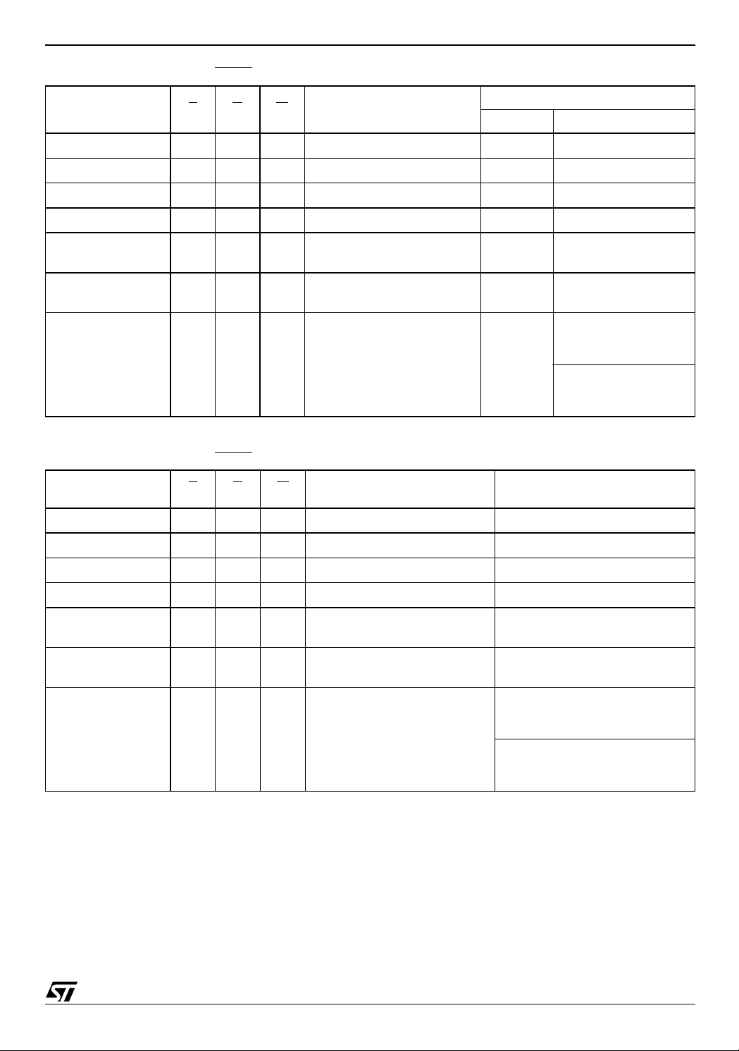
Table 2. Bus Operations, BYTE = V
Operation E G W
Bus Read
Bus Write
Output Disable X
Standby
Read Manufacturer
Code
Read Device Code
Extended Memory
Block Verify Code
Note: X = VIL or VIH.
V
V
V
V
V
V
V
IL
IL
IH
IL
IL
IL
IL
V
IH
V
IH
X X X Hi-Z Hi-Z
V
IL
V
IL
V
IL
Table 3. Bus Operations, BYTE = V
Operation E
Bus Read
Bus Write
Output Disable X
Standby
Read Manufacturer
Code
Read Device Code
Extended Memory
Block Verify Code
Note: X = VIL or VIH.
V
V
V
V
V
V
G W
V
IL
IL
IH
IL
IL
IL
IL
V
IH
V
IH
X X X Hi-Z
V
IL
V
IL
V
IL
IL
Address Inputs
DQ15A–1, A0-A21
V
Cell Address Hi-Z Data Output
IH
V
Command Address Hi-Z Data Input
IL
V
X Hi-Z Hi-Z
IH
A0 = VIL, A1 = VIL, A9 = VID,
V
IH
Others V
A0 = VIH, A1 = VIL,
V
IH
A9 = V
or V
IL
IH
, Others VIL or V
ID
DQ14-DQ8 DQ7-DQ0
IH
Data Inputs/Outputs
Hi-Z 20h
Hi-Z
DEh (M29W640DT)
DFh (M29W640DB)
98h (factory locked)
A0 = VIH, A1 = VIH, A6 = VIL,
V
IH
A9 = V
, Others VIL or V
ID
IH
Hi-Z
18h (not factory locked)
88h (factory locked)
08h (not factory locked)
IH
Address Inputs
A0-A21
V
Cell Address Data Output
IH
V
Command Address Data Input
IL
V
X Hi-Z
IH
A0 = VIL, A1 = VIL, A9 = VID,
V
IH
Others V
A0 = VIH, A1 = VIL, A9 = VID,
V
IH
Others V
IL
IL
or V
or V
IH
IH
Data Inputs/Outputs
DQ15A–1, DQ14-DQ0
22DEh (M29W640DT)
22DFh (M29W640DB)
M29W640DT
98h (factory locked)
A0 = VIH, A1 = VIH, A6 = VIL,
V
IH
A9 = V
, Others VIL or V
ID
IH
18h (not factory locked)
M29W640DB
88h (factory locked)
08h (not factory locked)
M29W640DT
M29W640DB
0020h
11/50

M29W640DT, M29W640DB
COMMAND INTERFACE
All Bus Write operations t o the me mory are in terpreted by the Command Interface. Commands
consist of one or more sequential Bus Write operations. Failure to observe a valid sequence of Bus
Write operations will result in the memory returning to Read mode. The long command sequences
are imposed to maximize data security.
The address used for the commands changes depending on whether the memory is in 16-bit or 8bit mode. See either Table 4, or Table 5, depending on the configuration that is being used, for a
summary of the commands.
Read/Reset Command.
The Read/Reset command returns the memory to
its Read mode where it behaves like a ROM or
EPROM. It also resets the errors in the Status
Register. Either one or three Bus Write operations
can be used to issue the Read/Reset command.
The Read/Reset command can be issued, between Bus Write cycles before the start of a program or erase operation, to return the device to
read mode. If the Read/Reset command is issued
during the timeout of a Block erase operation then
the memory will take up to 10µs to abort. During
the abort period no valid data can be read from the
memory. The Read/Reset command will not abort
an Erase operation when issued while in Erase
Suspend.
Auto Select Command.
The Auto Select command is used to read the
Manufacturer Code, the Device Code , the Block
Protection Status and the Extended Memory Block
Verify Code. Three c onsecutive Bus W rite operations are required to iss ue the Auto Select command. Once the Auto Select command is issued
the memory remains in Auto Select mode until a
Read/Reset command is issued. Read CFI Query
and Read/Reset comma nds are ac cept ed i n Aut o
Select mode, all other commands are ignored.
In Auto Select mode the Manufac turer Code can
be read using a Bus Read operation with A0 = V
and A1 = VIL. The other address bits may be set to
either V
Microelectronics is 0020h.
The Device Code can be read using a B us Read
operation with A0 = V
address bits may be set to e ither V
Device Code for the M29W640DT is 22DEh and
for the M29W640DB is 22DFh.
The Bl ock Prot ection S tatus of each block can be
read using a Bus Read operation with A0 = V
A1 = V
the bl ock. The oth er addr ess bit s may b e set t o either V
then 01h is output on Data Inputs/Outputs DQ0DQ7, otherwise 00h is output.
or VIH. The Manufacturer Code f or ST-
IL
and A1 = VIL. The other
IH
, and A 12 -A 21 spec ify i n g t he address of
IH
or VIH. If t h e ad dr ess ed b loc k is pro tec te d
IL
or VIH. The
IL
IL
Read CFI Query Command
The Read CFI Query Command is used to read
data from the Common Flash Interface (CFI)
Memory Area. This command is valid when the device is in the Read Array mode, or when the device
is in Autose lec ted mode .
One Bus Write cycle is required to issue the Read
CFI Query Command. Once the command is issued subsequent Bus Read ope rations read from
the Common Flash Interface Memory Area.
The Read/Reset command m ust be issued to return the device to the previous mode (the Read Array mode or Autoselected mode). A second Read/
Reset command would be needed if the device is
to be put in the Read Array mode from Autoselected mode.
See Appendix B, Table 21 to Table 26 for details
on the information contained in the Common Flash
Interface (CFI) memory area.
Program Command.
The Program command can be used to program a
value to one address in the memory array at a
time. The command requires four Bus Write operations, the final write operation latches the address and data, and starts the Program/Erase
Controller.
If the address falls in a pro tected block then the
Program command is ignored, the data remains
unchanged. The Status Register is never read and
no error condition is given.
During the program operat ion the memo ry will ignore all commands. I t is n ot poss ible t o iss ue any
command to abort or pause the operation. Typical
program times are given in Table 6. Bus Read operations during the program o peration will output
the Status Register on the Data Inputs/Outputs.
See the section on the S tatus Register for more
details.
After the program operation has completed the
memory will return to the Read mode, unle ss an
IL
error has occurred. When an error occurs the
memory will continue to output the Status Register. A Read/Reset command must be issued to reset the error condition and return to Read mode.
Note that the Program command cannot change a
bit set at ’0’ bac k to ’1’. One of the E rase Commands must be used to set all the bits in a block or
in the whole memory from ’0’ to ’1’.
Fast Program Commands
There are two Fast Program com man ds availa ble
,
to improve the programming throughput, by writing
several adjacent words or bytes in parallel. The
Quadruple Byte Program command is available for
x8 operations, while the Double Word Program
command is available for x16 operations.
12/50

M29W640DT, M29W640DB
Quadruple Byte Program Command. The Qua-
druple Byte Program command is used to write a
page of four adjacent Bytes in parallel. The four
bytes must differ only for addresses A0, DQ15A-1.
Five bus write cycles are necessary to issue the
Quadruple Byte Program command .
■ The first bus cycle sets up the Quadruple Byte
Program Command.
■ The second bus cycle latches the Address and
the Data of the first byte to be written.
■ The third bus cycle latches the Address and the
Data of the second byte to be written.
■ The fourth bus cycle latches the Address and
the Data of the third byte to be written.
■ The fifth bus cycl e latches the Addres s and th e
Data of the fourth byte to be written and starts
the Program/Erase Controller.
Double Word Program Command. The Double Word Program command is used to write a p age of two adjacent words in parallel. Th e two words must differ only for the address A0.
Three bus write cycles are necessary to issue the
Double Word Program command.
■ The first bus cycle sets up the Double Word
Program Command.
■ The second bus cycle latches the Address and
the Data of the first word to be written.
■ The third bus cycle latches the Address and the
Data of the second word to be written and starts
the Program/Erase Controller.
Only one bank can be programmed at any one
time. The other b ank must be in Read mode or
Erase Suspend.
Programming should not be attempted when V
is not at V
PPH
.
PP
After programming has started, Bus Read operations in the Bank being programmed output the
Status Register content, while Bus Read operations to the other B ank outpu t the cont ents of t he
memory ar ray.
After the program operation has completed the
memory will return to the Read mode, unle ss an
error has occurred. When an error occurs Bus
Read operations to the Bank where the command
was issued will continue to output the Status Register. A Read/Reset command must be issued to
reset the error condition and return t o Read mode.
Note that the Fast Program commands cannot
change a bit set at ’0’ back to ’1’. One of the Erase
Commands must be used to set all the bits in a
block or in the whole memory from ’0’ to ’1’.
Typical Program times are given in Tab le 6, Program, Erase Times and Program, Erase Endurance Cycles.
Unlock Bypass Command.
The Unlock Bypass command is used in conjunction with the Unlock Bypass Program command to
program the memory faster than with the standard
program commands. When th e cycle time to the
device is long (as with some EPROM programmers) considerable time saving can be m ade by
using these commands. Three Bus Write operations are required to issue the Unlock Bypass
command.
Once the Unlock Bypas s command has bee n issued the memory will only accept the Unloc k Bypass Program command and the Unlock Bypass
Reset command. The memory can be read as if in
Read mode.
When V
is applied to the VPP/Write Protect pin
PP
the memory automatically enters the Unlock Bypass mode and the Unlock Bypass Program command can be issued immediately.
Unlock Bypass Program Command.
The Unlock Bypass command is used in conjunction with the Unlock Bypass Program command to
program the memory. Whe n the cycle time t o the
device is long (as with some EPROM programmers) considerable time saving can be m ade by
using these commands. Three Bus Write operations are required to issue the Unlock Bypass
command.
Once the Unlock Bypas s command has bee n issued the memory will only accept the Unloc k Bypass Program command and the Unlock Bypass
Reset command. The memory can be read as if in
Read mode.
The memory offers accelerated program operations through the V
system asserts V
/Write Protect pin. When the
PP
on the VPP/Write Protect pin,
PP
the memory automatically enters the Unlock Bypass mode. The system may then write the twocycle Unlock Bypass program command sequence. The memory uses the higher voltage on
the V
/Write Protect pin, to accelerate the Unlock
PP
Bypass Program operation.
Never raise V
/Write Protect to VPP from any
PP
mode except Read m ode, otherwise the memory
may be left in an indeterminate state.
Unlock Bypass Reset Command.
The Unlock Bypass Rese t command can be used
to return to Read/Reset mode from Unlock Bypass
Mode. Two Bus Write operations are required to
issue the Unlock Bypass Reset command. Read/
Reset command does not exit from Unlock Bypass
Mode.
Chip Erase Command.
The Chip Erase command can be used to erase
the entire chip. Six Bus Write operations a re re-
13/50

M29W640DT, M29W640DB
quired to issue the Chip Erase Command and start
the Program/Erase Controller.
If any blocks are protected then these are ignored
and all the other blocks are erased. If all of the
blocks are protect e d th e Chip Erase op erat i on ap-
pears to start but will terminate within about 100µs,
leaving the data unchanged. No error condition is
given when protected blocks are ignored.
During the erase operation the memory will ignore
all commands, including the Erase Suspen d command. It is not possible to i ssue any c ommand t o
abort the operation. Typical chip erase tim es are
given in Table 6. All Bus Read operations during
the Chip Erase operation will output the Status
Register on the Data Inputs/Outputs. See the section on the Status Register for more details.
After the Chip Erase operation has completed t he
memory will return to the Read Mode, unle ss an
error has occurred. When an error occurs the
memory will continue to output the Status Register. A Read/Reset command must be issued to reset the error condition and return to Read Mode.
The Chip Erase Command sets all of the bits in unprotected blocks of the memory to ’1’. All previous
data is lost.
Block Erase Command.
The Block Erase com mand can be used to erase
a list of one or more blocks. Six Bus Write operations are required to select the first block in the li st.
Each additional block in the list can be selected by
repeating the sixth Bus Write operation using the
address of the additional block. The B lock Erase
operation starts the Program/Erase Controller
about 50µs after the last Bus Write operation.
Once the Pr ogram /Erase Co ntroller st arts it is not
possible to select any more blocks. Each additional block must therefore be selected within 50µs of
the last block. The 50µs timer restarts when an additional block is selected. The Status Register can
be read after the sixth B us Write operation. See
the Status Register section for details on how to
identify if the Program/ Erase Con troller has st arted the Block Erase operation.
If any selected blocks are protected then these are
ignored and all the other selected blocks are
erased. If all of the selected blocks are p rotected
the Block Erase operation appears to start but will
terminate within about 100µs, leaving the data unchanged. No error condition is given when protected blocks are ignored.
During the Block Erase operation the me mory wi ll
ignore all commands except the Erase Susp end
command. Typical b lock era se tim es are g iven in
Table 6. All Bus Read operations during the Block
Erase ope ra tion will outp ut the S t atus R e gister on
the Data Inputs/Outputs. See the section on the
Status Register for more details.
After the Block Erase operation has completed the
memory will return to the Read Mode, unle ss an
error has occurred. When an error occurs the
memory will continue to output the Status Register. A Read/Reset command must be issued to reset the error condition and return to Read mode.
The Block Erase Command sets all of the bits in
the unprotected selected blocks to ’1’. All previous
data in the selected blocks is lost.
Erase Suspend Command.
The Erase Suspend Command may be used to
temporarily suspend a B lock Eras e operation and
return the memory to Read mode. T he comm and
requires one Bus Write operation.
The Program/Erase Controller will sus pend within
the Erase Suspend Latency time of the Erase Suspend Command being issued. Once the Program/
Erase Controller has stopped the mem ory will be
set to Read mode and the E ras e wi ll be s uspended. If the Erase Suspend command is issued during the period when the memory is waiting for an
additional block (before the Program/Er ase Controller starts) then the Erase is suspended immediately and will start immediately when the Erase
Resume Command is issued. It is not possibl e to
select any further blocks to erase after the Erase
Resume.
During Erase Suspend it is possible to Read and
Program cells in blocks that are not being erased;
both Read and Program operations behave as
normal on these blocks. If any attempt is made to
program in a protected block or in the suspended
block then the Program comm and is ignored and
the data remains unchanged. The Status Register
is not read and no error condi tion is given. Reading from blocks that are being erased will output
the Status Register.
It is also possible to issue the Auto Select, Read
CFI Query and Unlock Bypass commands du ring
an Erase Suspend. The Read/Reset command
must be issued to return the device to Read Array
mode before the Resume command will be accepte d.
Erase Resume Command.
The Erase Resume command must be used to restart the Program/Erase Controller after an Erase
Suspend. The device must be in Read Array mode
before the Resume command will be accepted. An
erase can be suspe nded and resumed mo re t han
once.
Enter Extended Block Command
The device has an extra 64 KByte block (Extended
Block) that can on ly be acc essed usin g the Enter
Extended Block command. Three Bus write cycles
are required to issue the Extended Block command. Once the c ommand has been issued the
device enters Extended Block mode where all Bus
14/50

M29W640DT, M29W640DB
Read or Write operations to the Boot Block addresses access the Extended Bloc k. The Extended Block (with the same address as the Boot
Blocks) cannot be erased, and can be t reated as
one-time programmable (OTP) memory. In Extended Block mode the Boot Blocks are not accessible.
To exit from the Extended Block mode the Exit Extended Block command must be issued.
The Extended Block can be protected, however
once protected the protection cannot be undone.
Exit Extended Block Com m a n d
The Exit Extended Block command is used to exit
from the Extended Block mod e and ret urn the de-
vice to Read mode. Four Bus Write operations are
required to issue the command.
Block Protect and Chip Unprotect Commands
Groups of blocks can be protected against acci-
dental Program or Erase. The Protection Groups
are shown in Appendix A, T able 1 9 and T able 20,
Block Addresses. The whole chip can be unprotected to allow the data inside the blocks to be
changed.
Block Protect and Chip Unprote ct operations are
described in Appendix D.
15/50
 Loading...