

SGS Thomson Microelectronics M29W160BB90N1, M29W160BB70N1, M29W160BB, M29W160BT90N6, M29W160BT90N1 Datasheet
...
1/25
PRELIMINARY DATA
February 2000
This is preliminary information on a new product now in development or undergoing evaluation. Details are subject to change without notice.
M29W160BT
M29W160BB
16 Mbit (2Mb x8 or 1Mb x16, Boot Block)
Low Voltage Single Supply Flash Memory
■ SINGLE 2.7 to 3.6V SUPPLY VOLTAGE for
PROGRAM, ERASE and READ OPERATIONS
■ ACCESS TIME: 70ns
■ PROGRAMMING TIME
–10µs per Byte/Word typical
■ 35 MEMORYBLOCKS
– 1 Boot Block (Top or Bottom Location)
– 2 Parameter and 32 Main Blocks
■ PROGRAM/ERASE CONTROLLER
– Embedded Byte/Word Program algorithm
– Embedded Multi-Block/Chip Erase algorithm
– Status Register Polling and Toggle Bits
– Ready/Busy Output Pin
■ ERASE SUSPEND and RESUME MODES
– Read and Program another Block during
Erase Suspend
■ UNLOCKBYPASS PROGRAM COMMAND
– FasterProduction/Batch Programming
■ TEMPORARY BLOCK UNPROTECTION
MODE
■ SECURITY MEMORY BLOCK
■ LOW POWER CONSUMPTION
– Standby and Automatic Standby
■ 100,000 PROGRAM/ERASE CYCLES per
BLOCK
■ 20 YEARS DATA RETENTION
– Defectivity below 1 ppm/year
■ ELECTRONIC SIGNATURE
– Manufacturer Code: 0020h
– Top Device Code M29W160BT: 22C4h
– Bottom Device Code M29W160BB: 2249h
44
1
TSOP48(N)
12 x 20mm
SO44 (M)
LFBGA48 (ZA)
8 x 6 solder balls
FBGA
Figure 1. Logic Diagram
Note: RB not available on SO44 package.
AI00981
20
A0-A19
W
DQ0-DQ14
V
CC
M29W160BT
M29W160BB
E
V
SS
15
G
RP
DQ15A–1
BYTE
RB
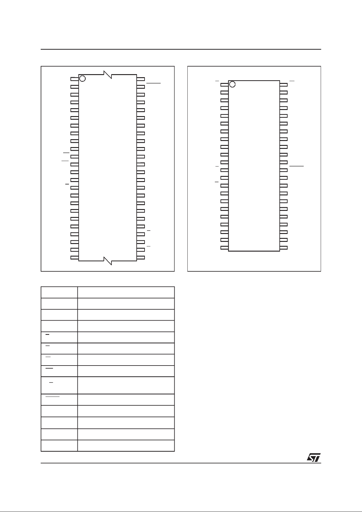
M29W160BT, M29W160BB
2/25
Figure 2. TSOP Connections
DQ3
DQ9
DQ2
A6
DQ0
W
A3
RB
DQ6
A8
A9
DQ13
A17
A10 DQ14
A2
DQ12
DQ10
DQ15A–1
V
CC
DQ4
DQ5
A7
DQ7
NC
NC
AI02994
M29W160BT
M29W160BB
12
1
13
24 25
36
37
48
DQ8
NC
A19
A1
A18
A4
A5
DQ1
DQ11
G
A12
A13
A16
A11
BYTE
A15
A14
V
SS
E
A0
RP
V
SS
Figure 3. SO Connections
G
DQ0
DQ8
A3
A0
E
V
SS
A2
A1
A13
V
SS
A14
A15
DQ7
A12
A16
BYTE
DQ15A–1
DQ5DQ2
DQ3
V
CC
DQ11
DQ4
DQ14
A9
A19
RP
A4
W
A7
AI00978
M29W160BT
M29W160BB
8
2
3
4
5
6
7
9
10
11
12
13
14
15
16
32
31
30
29
28
27
26
25
24
2322
20
19
18
17DQ1
DQ9
A6
A5
DQ6
DQ13
44
39
38
37
36
35
34
33
A11
A10
DQ10
21
DQ12
40
43
1
42
41
A17 A8
A18
Table 1. Signal Names
A0-A19 Address Inputs
DQ0-DQ7 Data Inputs/Outputs
DQ8-DQ14 Data Inputs/Outputs
DQ15A–1 Data Input/Output or Address Input
E Chip Enable
G Output Enable
W Write Enable
RP Reset/Block Temporary Unprotect
RB
Ready/Busy Output
(Not availableon SO44 package)
BYTE Byte/Word Organization Select
V
CC
Supply Voltage
V
SS
Ground
NC Not Connected Internally
DU Don’t Use as internally connected
3/25
M29W160BT, M29W160BB
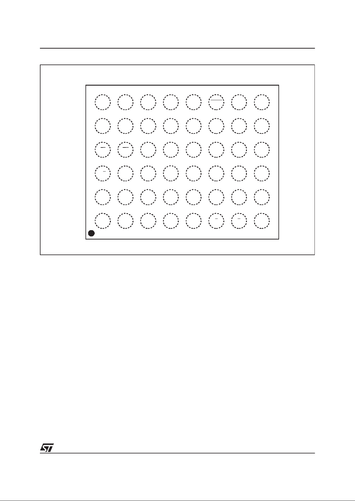
Figure 4. LFBGA Connections (Top view through package)
AI02985B
D
E
F
87654321
B
C
A
V
SS
DQ15
A–1
A15A14A12A13
DQ3DQ11DQ10A18DURB
DQ1DQ9DQ8DQ0A6A17A7
GEA0 A4A3
DQ2
DQ6DQ13DQ14A10A8A9
DQ4V
CC
DQ12DQ5A19DURPW
A11 DQ7
A1 A2 V
SS
A5
DU
A16
BYTE
M29W160BT, M29W160BB
4/25
SUMMARY DESCRIPTION
The M29W160B is a 16 Mbit (2Mb x8 or 1Mb x16)
non-volatile memory that can be read, erased and
reprogrammed. These operations can be performed using a single low voltage (2.7 to 3.6V)
supply. On power-up the memory defaults to its
Read mode where it can be read in the same way
as a ROM or EPROM.
The memory is divided into blocks that can be
erased independently so it is possible to preserve
valid data while old data is erased.Each block can
be protected independently to prevent accidental
Program or Erase commands from modifying the
memory. Program and Erase commands are written to the Command Interface of the memory. An
on-chip Program/Erase Controller simplifies the
process ofprogramming or erasing the memory by
taking care of all of the special operations that are
required to update the memory contents.
Table 2. Absolute Maximum Ratings
(1)
Note: 1. Except for the rating ”Operating Temperature Range”, stresses above those listed in the Table ”Absolute Maximum Ratings” may
cause permanent damage to the device. These are stress ratings only and operation of the device atthese or any other conditions
above those indicated in the Operating sections of this specification is not implied. Exposure to Absolute Maximum Rating conditions forextended periods may affect device reliability. Refer also tothe STMicroelectronics SURE Program and other relevant quality documents.
2. Minimum Voltage may undershoot to –2V during transition and for less than 20ns during transitions.
Symbol Parameter Value Unit
T
A
Ambient Operating Temperature (Temperature Range Option 1) 0 to 70 °C
Ambient Operating Temperature (Temperature Range Option 6) –40 to 85 °C
T
BIAS
Temperature Under Bias –50 to 125 °C
T
STG
Storage Temperature –65 to 150 °C
V
IO
(2)
Input or Output Voltage –0.6 to 4 V
V
CC
Supply Voltage –0.6 to 4 V
V
ID
Identification Voltage –0.6 to 13.5 V
The end of a program or erase operation can be
detected and any error conditions identified. The
command set required to control the memory is
consistent with JEDEC standards.
The blocks in the memory are asymmetrically arranged, seeTables 3 and 4, Block Addresses. The
first or last 64 Kbytes have been divided into four
additional blocks. The16 Kbyte Boot Block can be
used for small initialization code to start themicroprocessor, the two 8 Kbyte Parameter Blocks can
be used for parameter storage and the remaining
32K is a small Main Block where the application
may be stored.
Chip Enable, Output Enable andWrite Enable signals control the bus operation of the memory.
They allow simple connection to most microprocessors, often without additional logic.
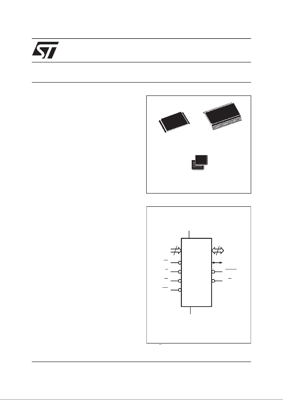
The memory is offered in TSOP48 (12 x 20mm),
SO44 and LFBGA48 (0.8mm pitch) packagesand
it is supplied with all the bits erased (set to ’1’).
5/25
M29W160BT, M29W160BB
Table 3. Top Boot Block Addresses,
M29W160BT
#
Size
(Kby t es)
AddressRange
(x8)
Addres sRange
(x16)
34 16 1FC000h-1FFFFFh FE000h-FFFFFh
33 8 1FA000h-1FBFFFh FD000h-FDFFFh
32 8 1F8000h-1F9FFFh FC000h-FCFFFh
31 32 1F0000h-1F7FFFh F8000h-FBFFFh
30 64 1E0000h-1EFFFFh F0000h-F7FFFh
29 64 1D0000h-1DFFFFh E8000h-EFFFFh
28 64 1C0000h-1CFFFFh E0000h-E7FFFh
27 64 1B0000h-1BFFFFh D8000h-DFFFFh
26 64 1A0000h-1AFFFFh D0000h-D7FFFh
25 64 190000h-19FFFFh C8000h-CFFFFh
24 64 180000h-18FFFFh C0000h-C7FFFh
23 64 170000h-17FFFFh B8000h-BFFFFh
22 64 160000h-16FFFFh B0000h-B7FFFh
21 64 150000h-15FFFFh A8000h-AFFFFh
20 64 140000h-14FFFFh A0000h-A7FFFh
19 64 130000h-13FFFFh 98000h-9FFFFh
18 64 120000h-12FFFFh 90000h-97FFFh
17 64 110000h-11FFFFh 88000h-8FFFFh
16 64 100000h-10FFFFh 80000h-87FFFh
15 64 0F0000h-0FFFFFh 78000h-7FFFFh
14 64 0E0000h-0EFFFFh 70000h-77FFFh
13 64 0D0000h-0DFFFFh 68000h-6FFFFh
12 64 0C0000h-0CFFFFh 60000h-67FFFh
11 64 0B0000h-0BFFFFh 58000h-5FFFFh
10 64 0A0000h-0AFFFFh 50000h-57FFFh
9 64 090000h-09FFFFh 48000h-4FFFFh
8 64 080000h-08FFFFh 40000h-47FFFh
7 64 070000h-07FFFFh 38000h-3FFFFh
6 64 060000h-06FFFFh 30000h-37FFFh
5 64 050000h-05FFFFh 28000h-2FFFFh
4 64 040000h-04FFFFh 20000h-27FFFh
3 64 030000h-03FFFFh 18000h-1FFFFh
2 64 020000h-02FFFFh 10000h-17FFFh
1 64 010000h-01FFFFh 08000h-0FFFFh
0 64 000000h-00FFFFh 00000h-07FFFh
Table 4. Bottom Boot Block Addresses,
M29W160BB
#
Size
(Kbytes)
Address Range
(x8)
Address Range
(x16)
34 64 1F0000h-1FFFFFh F8000h-FFFFFh
33 64 1E0000h-1EFFFFh F0000h-F7FFFh
32 64 1D0000h-1DFFFFh E8000h-EFFFFh
31 64 1C0000h-1CFFFFh E0000h-E7FFFh
30 64 1B0000h-1BFFFFh D8000h-DFFFFh
29 64 1A0000h-1AFFFFh D0000h-D7FFFh
28 64 190000h-19FFFFh C8000h-CFFFFh
27 64 180000h-18FFFFh C0000h-C7FFFh
26 64 170000h-17FFFFh B8000h-BFFFFh
25 64 160000h-16FFFFh B0000h-B7FFFh
24 64 150000h-15FFFFh A8000h-AFFFFh
23 64 140000h-14FFFFh A0000h-A7FFFh
22 64 130000h-13FFFFh 98000h-9FFFFh
21 64 120000h-12FFFFh 90000h-97FFFh
20 64 110000h-11FFFFh 88000h-8FFFFh
19 64 100000h-10FFFFh 80000h-87FFFh
18 64 0F0000h-0FFFFFh 78000h-7FFFFh
17 64 0E0000h-0EFFFFh 70000h-77FFFh
16 64 0D0000h-0DFFFFh 68000h-6FFFFh
15 64 0C0000h-0CFFFFh 60000h-67FFFh
14 64 0B0000h-0BFFFFh 58000h-5FFFFh
13 64 0A0000h-0AFFFFh 50000h-57FFFh
12 64 090000h-09FFFFh 48000h-4FFFFh
11 64 080000h-08FFFFh 40000h-47FFFh
10 64 070000h-07FFFFh 38000h-3FFFFh
9 64 060000h-06FFFFh 30000h-37FFFh
8 64 050000h-05FFFFh 28000h-2FFFFh
7 64 040000h-04FFFFh 20000h-27FFFh
6 64 030000h-03FFFFh 18000h-1FFFFh
5 64 020000h-02FFFFh 10000h-17FFFh
4 64 010000h-01FFFFh 08000h-0FFFFh
3 32 008000h-00FFFFh 04000h-07FFFh
2 8 006000h-007FFFh 03000h-03FFFh
1 8 004000h-005FFFh 02000h-02FFFh
0 16 000000h-003FFFh 00000h-01FFFh

M29W160BT, M29W160BB
6/25
SIGNAL DESCRIPTIONS
See Figure 1, Logic Diagram, and Table 1, Signal
Names, fora brief overview ofthesignals connected to this device.
Address Inputs (A0-A19). The Address Inputs
select the cells in the memoryarray to access during Bus Read operations. During BusWrite operations they control the commands sent to the
Command Interface of the internal state machine.
Data Inputs/Outputs (DQ0-DQ7). The Data Inputs/Outputs outputthe datastored at the selected
address during a Bus Readoperation. DuringBus
Write operations they represent the commands
sent tothe Command Interface of theinternal state
machine.
Data Inputs/Outputs (DQ8-DQ14). The Data Inputs/Outputs outputthe datastored at the selected
address during a Bus Read operation when BYTE
is High, VIH. When BYTE is Low, VIL, these pins
are not used and arehigh impedance. During Bus
Write operations the Command Register does not
use these bits. When reading the Status Register
these bits should be ignored.
Data Input/Output or Address Input (DQ15A-1).
When BYTE is High, VIH, this pin behaves as a
Data Input/Output pin (as DQ8-DQ14). When
BYTE is Low, VIL, this pin behaves asan address
pin; DQ15A–1 Low willselect the LSB of the Word
on the other addresses, DQ15A–1 Highwill select
the MSB. Throughout the text consider references
to the Data Input/Output to include this pin when
BYTE is High and references to the Address Inputs to include this pin when BYTE is Low except
when stated explicitly otherwise.
Chip Enable (E). The Chip Enable, E, activates
the memory,allowing BusRead and Bus Writeoperations to be performed. When Chip Enable is
High, VIH, all other pins are ignored.
Output Enable (G). The Output Enable, G, controls the Bus Read operation of the memory.
Write Enable (W). The Write Enable, W, controls
the Bus Write operation of the memory’s Command Interface.
Reset/Block Temporary Unprotect (RP). The
Reset/Block Temporary Unprotect pin can be
used to apply a Hardware Resetto the memory or
to temporarily unprotect all Blocks that have been
protected.
A Hardware Reset is achieved by holding Reset/
Block Temporary Unprotect Low, VIL, for at least
t
PLPX
. After Reset/Block Temporary Unprotect
goes High, VIH, the memory will be ready for Bus
Read and Bus Write operations after t
PHEL
or
t
RHEL
, whicheveroccurs last. See the Ready/Busy
Output section, Table 18 and Figure 12, Reset/
Temporary Unprotect AC Characteristics for more
details.
Holding RP at VIDwill temporarily unprotect the
protected Blocks in the memory. Program and
Erase operations on all blocks will be possible.
The transition from VIHtoVIDmustbe slower than
t
PHPHH
.
Ready/Busy Output (RB). The Ready/Busy pin
is anopen-drain output that can be used to identify
when the memory array can be read. Ready/Busy
is high-impedance during Read mode, Auto Select
mode and Erase Suspend mode.
After a Hardware Reset, Bus Read and Bus Write
operations cannot begin until Ready/Busy becomes high-impedance. See Table 18 and Figure
12, Reset/Temporary Unprotect AC Characteristics.
During Program or Erase operations Ready/Busy
is Low, VOL. Ready/Busy will remain Low during
Read/Reset commands or Hardware Resets until
the memory is ready to enter Read mode.
The use ofan open-drain output allowsthe Ready/
Busy pins from several memories to be connected
to asingle pull-up resistor. A Low will then indicate
that one, or more, of the memories is busy.
Byte/Word Organization Select (BYTE). The
Byte/Word Organization Select pin is used to
switch between the 8-bit and 16-bit Bus modes of
the memory. When Byte/Word Organization Select isLow, VIL, the memory is in 8-bit mode, when
it is High, VIH, the memory is in 16-bit mode.
VCCSupply Voltage. The VCCSupply Voltage
supplies the power for all operations (Read, Program, Erase etc.).
The Command Interface is disabledwhen the V
CC
Supply Voltage is less than the Lockout Voltage,
V
LKO
. Thisprevents Bus Write operationsfrom accidentally damaging the data during power up,
power down and power surges. If the Program/
Erase Controller is programming orerasing during
this time thenthe operation aborts and the memory contents being altered will be invalid.
A 0.1µF capacitor should be connected between
the VCCSupply Voltage pin and the VSSGround
pin to decouplethe current surges from the power
supply. The PCB track widthsmust be sufficient to
carry the currents required during program and
erase operations, I
CC3
.
Vss Ground. The VSSGround is the reference
for all voltage measurements.
7/25
M29W160BT, M29W160BB
Table 5. Bus Operations, BYTE = V
IL
Note: X = VILor VIH.
Table 6. Bus Operations, BYTE = V
IH
Note: X = VILor VIH.
Operation E G W
Address Inputs
DQ15A–1, A0-A19
Data Inputs/Outputs
DQ14-DQ8 DQ7-DQ0
Bus Read
V
IL
V
IL
V
IH
Cell Address Hi-Z Data Output
Bus Write
V
IL
V
IH
V
IL
Command Address Hi-Z Data Input
Output Disable X
V
IH
V
IH
X Hi-Z Hi-Z
Standby
V
IH
X X X Hi-Z Hi-Z
Read Manufacturer
Code
V
IL
V
IL
V
IH
A0 = VIL,A1=VIL,A9=VID,
Others V
IL
or V
IH
Hi-Z 20h
Read Device Code
V
IL
V
IL
V
IH
A0 = VIH,A1=VIL,A9=VID,
Others V
IL
or V
IH
Hi-Z
C4h (M29W160BT)
49h (M29W160BB)
Operation E G W
Address Inputs
A0-A19
Data Inputs/Outputs
DQ15A–1, DQ14-DQ0
Bus Read
V
IL
V
IL
V
IH
Cell Address Data Output
Bus Write V
IL
V
IH
V
IL
Command Address Data Input
Output Disable X V
IH
V
IH
X Hi-Z
Standby
V
IH
X X X Hi-Z
Read Manufacturer
Code
V
IL
V
IL
V
IH
A0 = VIL,A1=VIL,A9=VID,
Others V
IL
or V
IH
0020h
Read Device Code
V
IL
V
IL
V
IH
A0 = VIH,A1=VIL,A9=VID,
Others V
IL
or V
IH
22C4h (M29W160BT)
2249h (M29W160BB)
BUS OPERATIONS
There are five standardbusoperations that control
the device. These are Bus Read, Bus Write, Output Disable, Standby and Automatic Standby. See
Tables 5 and 6, Bus Operations, for a summary.
Typically glitches of less than 5ns on Chip Enable
or WriteEnable areignored by the memory and do
not affect bus operations.
Bus Read. Bus Read operations read from the
memory cells, or specific registers in the Command Interface. A valid Bus Read operation involves setting the desiredaddress on the Address
Inputs, applying a Low signal, VIL, to Chip Enable
and Output Enable and keeping Write Enable
High, VIH. The Data Inputs/Outputs will output the
value, see Figure 9, Read Mode AC Waveforms,
and Table15, Read ACCharacteristics, for details
of when the output becomes valid.
Bus Write. Bus Write operations write to the
Command Interface. A valid Bus Write operation
begins by setting the desired address on the Address Inputs. The Address Inputs are latched by
the Command Interface onthe falling edgeof Chip
Enable or Write Enable, whichever occurs last.
The Data Inputs/Outputs are latched by the Command Interface on the rising edge of Chip Enable
or Write Enable,whichever occursfirst.OutputEnable must remain High, VIH, during the whole Bus
Write operation. See Figures 10 and 11, Write AC
Waveforms, and Tables 16 and 17, Write AC
Characteristics, for details of the timing requirements.

M29W160BT, M29W160BB
8/25
Output Disable. The Data Inputs/Outputs are in
the high impedance state when Output Enable is
High, VIH.
Standby. When Chip Enable is High, VIH, the
memory enters Standby mode and the Data Inputs/Outputs pins are placed in the high-impedance state. To reduce the Supply Current to the
Standby Supply Current, I
CC2
, ChipEnable should
be held within VCC± 0.2V. For the Standby current
level see Table 14, DC Characteristics.
During program or erase operations the memory
will continue to use the Program/Erase Supply
Current, I
CC3
, forProgram or Erase operations un-
til the operation completes.
AutomaticStandby. If CMOSlevels (VCC± 0.2V)
are usedto drive thebus and the busis inactivefor
150ns or more the memory enters Automatic
Standby where the internal Supply Current is reduced to the Standby Supply Current, I
CC2
. The
Data Inputs/Outputs will still output data if a Bus
Read operation is in progress.
Special Bus Operations
Additional bus operations can be performed to
read the Electronic Signature and also to apply
and remove Block Protection. These bus operations are intended for use by programming equipment and are not usually used in applications.
They require VIDto be applied to some pins.
Electronic Signature. The memory has two
codes, the manufacturer code and the device
code, that can be read to identify the memory.
These codes can be read by applying the signals
listed in Tables 5 and 6, Bus Operations.
BlockProtection andBlocks Unprotection. Each
block can be separately protected against accidental Program or Erase. Protected blocks can be
unprotected to allow data to be changed.
There are two methods available for protecting
and unprotecting the blocks, one for use on programming equipment and the other for in-system
use. For further information refer to Application
Note AN1122, Applying Protection and Unprotection to M29 Series Flash.
COMMAND INTERFACE
All Bus Write operations to the memory are interpreted by the Command Interface. Commands
consist of one or more sequential Bus Write operations. Failure to observe a valid sequence of Bus
Write operations will result in the memory returning to Read mode. The long command sequences
are imposed to maximize data security.
The address used for the commandschanges depending on whether the memory is in 16-bit or 8bit mode. See either Table 7, or 8, depending on
the configurationthat isbeing used, for a summary
of the commands.
Read/Reset Command. The Read/Reset command returns the memory to its Readmode where
it behaves like a ROM or EPROM, unless stated
otherwise (see Security Data command). It also
resets the errors in theStatus Register. Either one
or three Bus Writeoperations canbe used to issue
the Read/Reset command.
If the Read/Reset command is issued during a
Block Erase operation orfollowing a Programming
or Erase errorthen the memory will take upto 10µs
to abort. During the abort period no valid data can
be read from the memory. Issuing a Read/Reset
command during a Block Erase operation will
leave invalid data in the memory.
Auto Select Command. The Auto Select command is used to read the Manufacturer Code, the
Device Code and the Block Protection Status.
Three consecutive Bus Write operations are required to issue the Auto Select command. Once
the Auto Select command is issued the memory
remains in Auto Select mode until another command is issued.
From the Auto Select mode the Manufacturer
Code can be read using a Bus Read operation
with A0 = VILandA1 = VIL. The otheraddress bits
may be set to either VILor VIH. The Manufacturer
Code for STMicroelectronics is 0020h.
The Device Code can be read using a Bus Read
operation with A0 = VIHand A1 = VIL. The other
address bits may be set to either VILor VIH. The
Device Code for the M29W160BT is 22C4h and
for the M29W160BB is 2249h.
The Block Protection Status of each block can be
read using a Bus Read operation with A0 = VIL,
A1 = VIH, and A12-A19 specifying the address of
the block. The other address bits may be set toeither VILor VIH. If the addressed block is protected then 01h is output on Data Inputs/Outputs
DQ0-DQ7, otherwise 00h is output.
Program Command. The Program command
can be used to program a value to one address in
the memory array at a time. The command requires four Bus Write operations,the final write operation latches theaddress and data inthe internal
state machine and starts the Program/Erase Controller.
If the address falls in a protected block then the
Program command is ignored, the data remains
unchanged. The Status Register isnever readand
no error condition is given.
During the program operation the memory will ignore all commands. It is not possible to issue any
command to abort or pause the operation. Typical
program times are given in Table 10. Bus Read
operations during the program operation will output the Status Register on the Data Inputs/Outputs. See the section on the Status Register for
more details.
 Loading...