

SGS Thomson Microelectronics M29W008AT120N1, M29W008AT, M29W008AB120N6T, M29W008AB120N6, M29W008AB120N1 Datasheet
...
1/30March 2000
M29W008AT
M29W008AB
8 Mbit (1Mb x8, Boot Block)
Low Voltage Single Supply Flash Memory
■ 2.7V to 3.6V SUPPLY VOLTAGE for
PROGRAM, ERAS E and READ O PER AT IONS
■ ACCESS TIME: 80ns
■ PROGRAMMING TIME: 10µs typical
■ PROGRAM/ERASE CONTROLLER (P/E.C.)
– Program Byte-by-Byte
– Status Register bits and Ready/Busy Output
■ SECURITY PROTECTION MEMORY AREA
■ INSTRUCTIONS ADDRESS CODING: 3 digits
■ MEMORY BLOCKS
– Boot Block (Top or Bottom location)
– Parameter and Main blocks
■ BLOCK, MULTI-BLOCK and CHIP ERASE
■ MULTI BLOCK PROTECTION/TEMPO R ARY
UNPROTECTION MODES
■ ERASE SUSPEND and RESUME MODES
– Read and Program another Block during
Erase Suspend
■ LOW POWER CONSUMPTION
– Stand-by and Automatic Stand-by
■ 100,000 PROGRAM/ER ASE CYCL ES per
BLOCK
■ 20 YEARS DATA RETENTI ON
– Defectivity below 1ppm/year
■ ELECTRONIC SIGNATURE
– Manufacturer Code: 20h
– Top Device Code, M29W008AT: D2h
– Bottom Device Code, M29W008AB: DCh
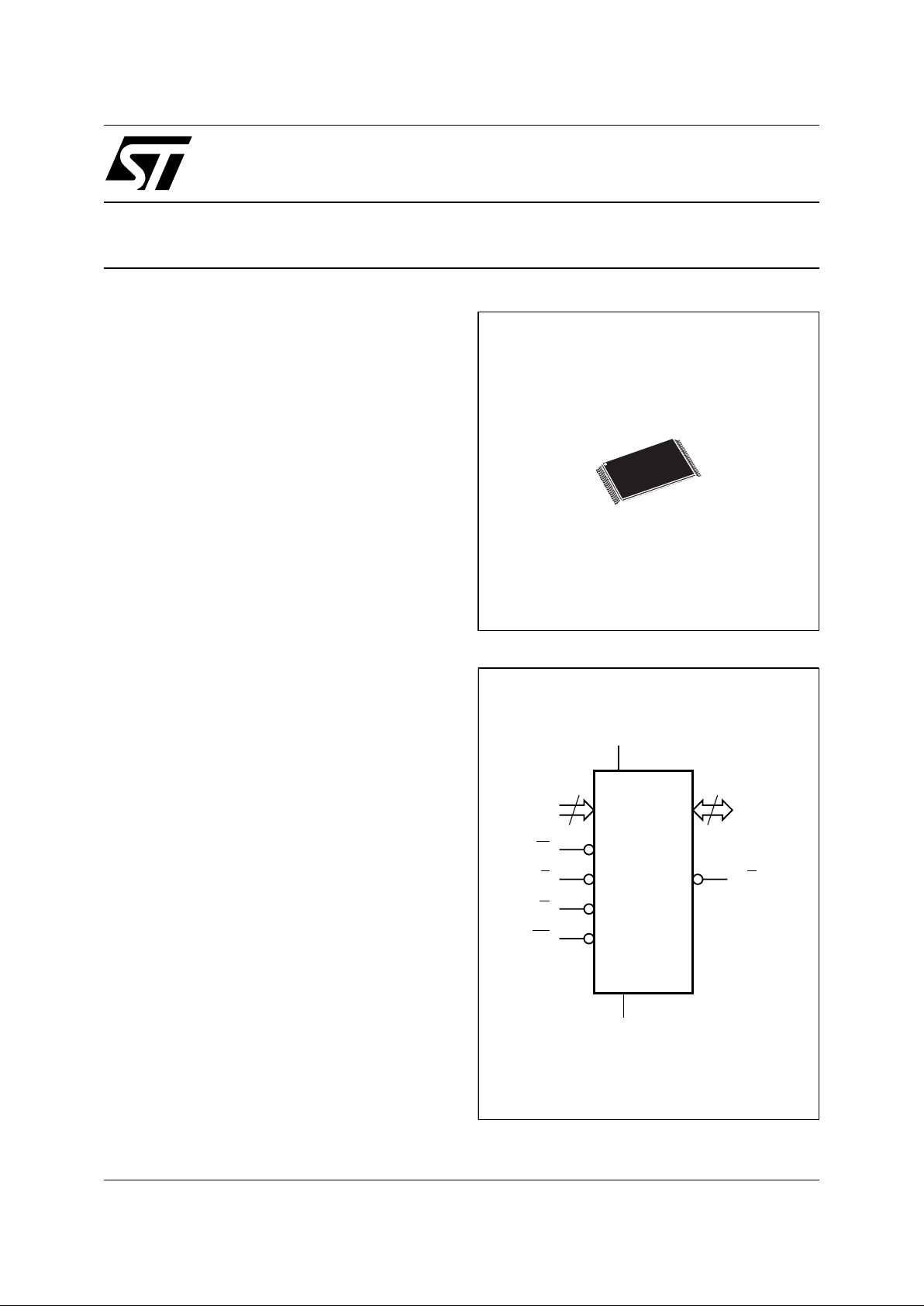
Figure 1. Logic Diagram
AI02716
20
A0-A19
W
DQ0-DQ7
V
CC
M29W008AT
M29W008AB
E
V
SS
8
G
RP
RB
TSOP40 (N)
10 x 20mm
M29W008AT, M29W008AB
2/30
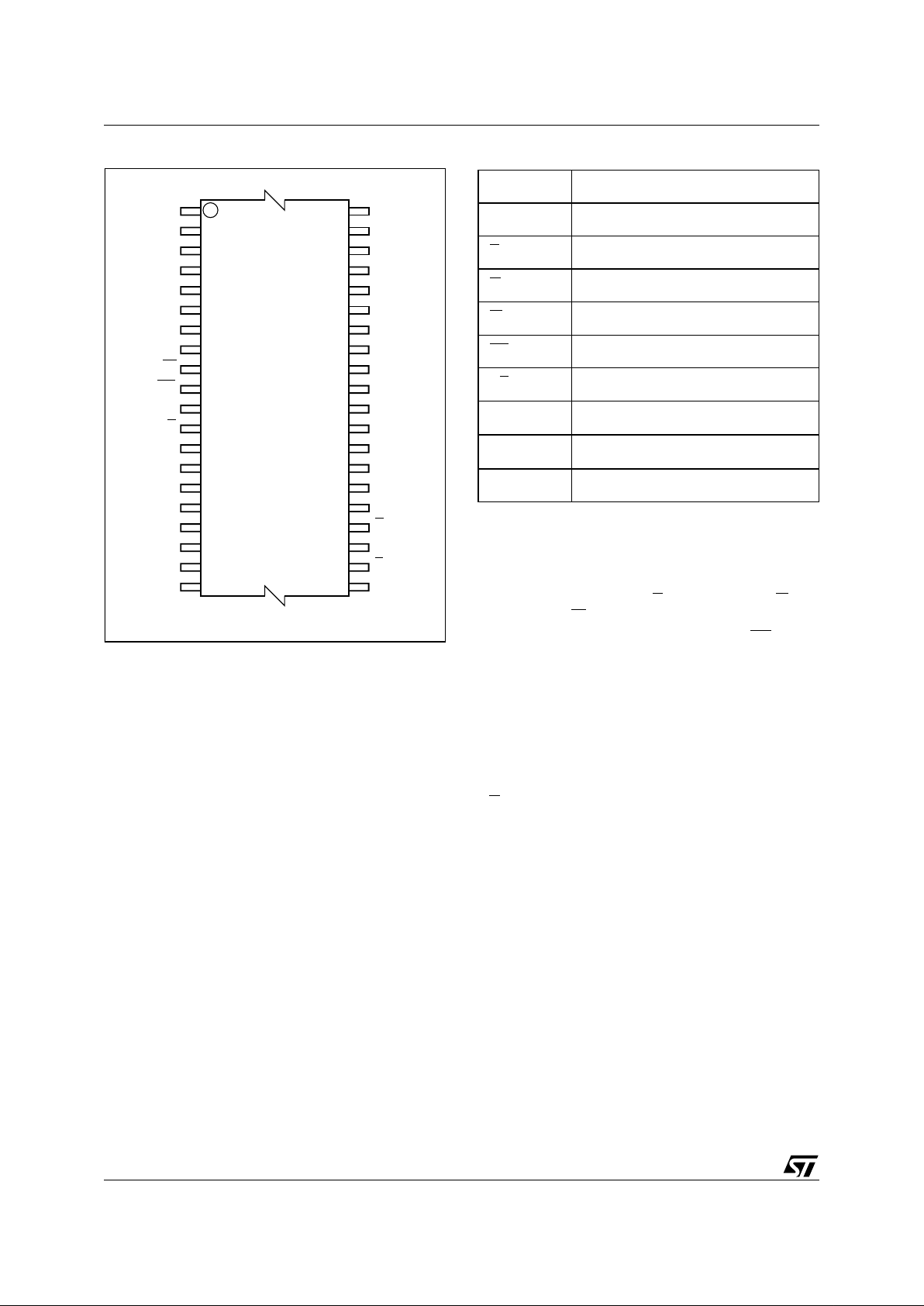
Figure 2. TSOP Connection s
V
SS
DQ1
DQ2A7
A1
E
A4
A3
A11
A17
A14
A15
DQ7
A9
A16
G
NC
DQ5
DQ3
NC
V
CC
DQ4
DQ6
A8
W
RB
A18
NC
RP
AI02717
M29W008AT
M29W008AB
10
1
11
20 21
30
31
40
A0
A12
A13
A19
A10
A5
A6
V
CC
DQ0
V
SS
A2
Table 1. Signal Names
A0-A19 Address Inputs
DQ0-DQ7 Data Input/Outputs, Command Inputs
E
Chip Enable
G
Output Enable
W
Write Enable
RP
Reset/Block Temporary Unprotect
RB
Ready/Busy Output
V
CC
Supply Voltage
V
SS
Ground
NC Not Connected Internally
Organisation
The M29W008A is organised as 1Mb x8. The
memory uses the addre ss inputs A0-A 19 and the
Data Input/Outputs DQ0-DQ7. Memory c ontrol is
provided by Chip Enable E
, Output Enable G and
Write Enable W
inputs.
A Reset/Block Temporary Unprotection RP
tri-level input provides a hardware reset when pulled
Low, and when held High (at V
ID
) temporarily unprotects bl ocks previo usly protecte d allowin g them
to be programed an d eras ed. E ras e and P rogram
operations are controlled by an internal Program/
Erase Controller (P/E.C.). Status Register data
output on DQ7 provides a Data Polling signal, and
DQ6 and DQ2 provide Toggle signals to indicate
the state of the P/E.C opera tions. A Ready/Busy
RB
output indicates the completion of the internal
algorithms.
Memory Blocks
The devices feature asymmetrically blocked architecture providing system memory integration. Both
M29W008AT and M29W0 08AB devices have an
array of 19 blocks, one Boot Block of 16 Kbytes,
two Parameter Blocks of 8 Kbytes, one Main Block
of 32 Kbytes and fifteen Main Blocks of 64 Kbytes.
The M29W008AT has the Boot Block at the top of
the memory address space and the M29W008AB
locates the Boot Block s tar ting at t he bot tom. The
memory maps are showed i n Tables 3, 4. Each
block can be e rased sepa rately, any combi nation
of blocks can be specified for mult i-block erase or
the entire chip may be erased . The Erase operations are managed automatically by the P/E.C.
DESCRIPTION
The M29W008A is a non-volatile memory that may
be erased electrically at the block or chip level and
programmed in-system on a Byte-by-Byte basis
using only a single 2.7V to 3.6V V
CC
supply. For
Program and Erase operations the necessary high
voltages are generated internally. The device can
also be programmed in standard programmers.
The array matrix organisation allows each block to
be erased and reprogrammed without affecting
other blocks. Bl ocks can be pro tected a gainst pro graming and erase on programming equipment,
and temporarily unprotected to make changes in
the application. Each block can be programmed
and erased over 100,000 cycles.
Instructions for Read/Reset, Auto Select for reading the Electronic Signature or Block Protection
status, Programming, Block and Chip Erase,
Erase Suspend and Resume are written to the device in cycles of comm ands to a Command Interface using standard microprocessor write timings.
The device is offered in TSOP40 (10 x 20mm)
package.
3/30
M29W008AT, M29W008AB
Instructions
Seven instructions are defined to perform Read
Array, Auto Select (to read the Electronic Signature or Block Protection Status), Program, Block
Erase, Chip Erase, Erase Suspend and Erase Resume. The internal P/E.C. automatically handles
all timing and verification of the Program and
Erase operations. The Status Regist er Data Polling, Toggle, Error bits and the RB
output may be
read at any time, during programming or erase, to
monitor the progress of the operation.
Instructi ons a re co mpose d of up to si x cycles. The
first two cycles input a Coded sequence to the
Command Interface which is common to all instructions (s ee Tab le 9). The third cycle inputs the
instruction set-up command. Subsequent cycles
output the addressed data, Electronic Signature or
Block Protection Status for Read operations. In order to give additional data protection, the instructi ons f or Pr ogram an d Block or Chip Eras e requir e
further command inputs. For a Program instruction, the fourth command cycle inputs the address
and data to be programmed. For an Erase instruction (Block or Chip), the fourth and fifth cycles input a further Coded sequence before the Erase
confirm command on the sixt h cy cle. Erasure of a
memory block may be suspended, in order to read
data from another block or to program d ata in another block, and then resumed.
When power is first applied or if V
CC
falls below V
L-
KO
, the command interface is reset to Read Array.
The block erase operation can be s uspended in
order to read from or program to any block not being erased, and then resumed.
Block protection provides additional data security.
Each block can be s eparately prot ec ted or unprotected against Program or Erase on programming
equipment. All previously protected blocks can be
temporarily unprotected in the application.
Bus Operations
The following operations can be performed using
the appropriate bus cycles: Read (Array, Electronic Signature, Block Protection Status ), W rite command, Output Disable, Stand-by, Reset, Block
Protection, Unprotection, Protection Verify, Unprotection Verify and Block Temporary Un protection.
See Tables 5 and 6.
Command Interface
Instructions, made up of commands wri tten in cycles, can be given to the Program/Erase Controller
through a Command Interface (C.I.). For added
data protection, program or erase execution starts
after 4 or 6 cycles. The first, second, fourth and
fifth cycles are used to input Coded c ycles to the
C.I. This Coded sequence is the same for all Program/Erase Controller instructions. The ’Command’ itself and its confirmation, when applicable,
are given on the third, fourth or sixth cycles. Any
incorrect command or any improper command sequence will reset the device to Read Array mode.
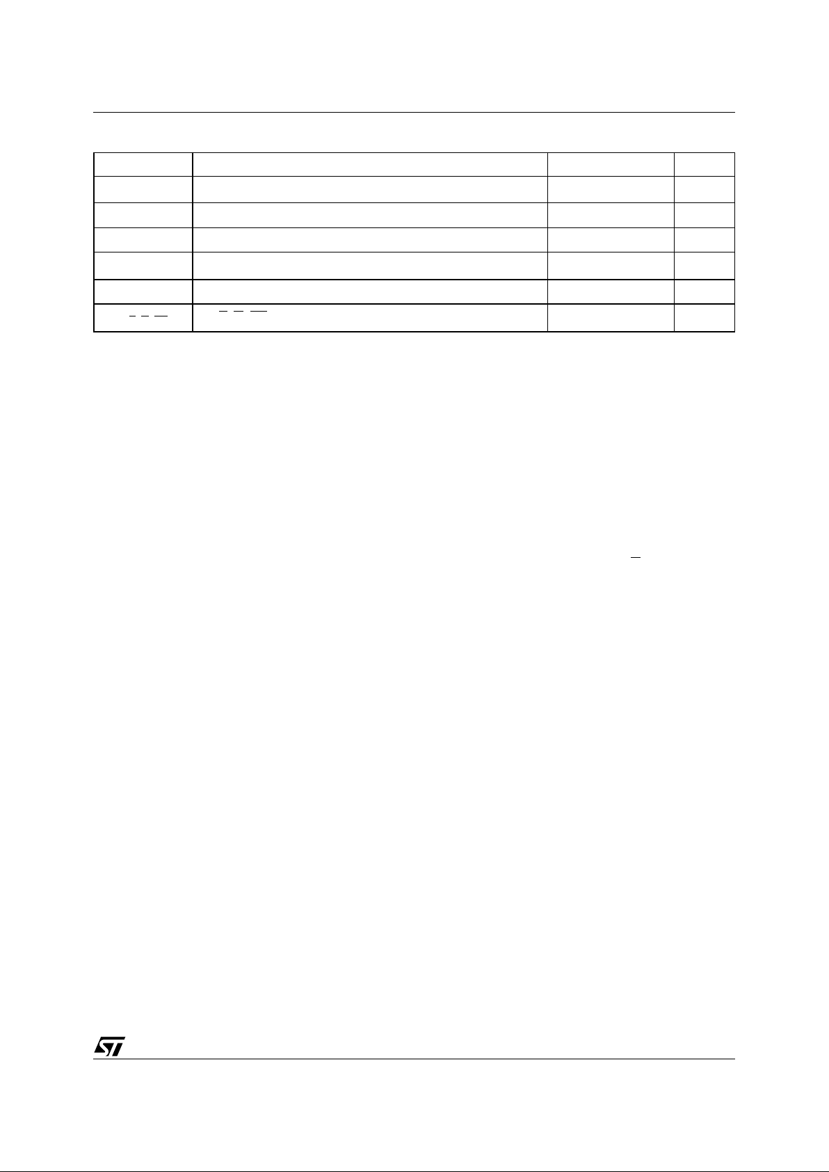
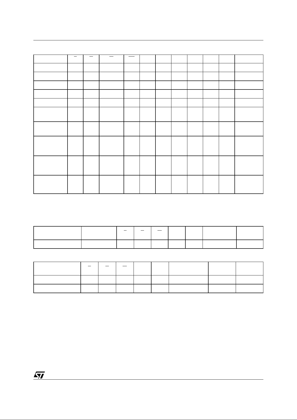
Table 2. Absolute Maximum Ratings
(1)
Note: 1. Except for the rating "Operating Temperature Range", s tresses above thos e l i sted in the Table "A bsolute M aximum Ratings" may
cause permanent damage to the device. These are stress ratings only and operation of the device at these or any other conditions
above those indi cated in the Operating sections of this s pecification is not impli ed. Exposure to A bsolute M aximum Rating conditions for extended per iods may aff ect device reliabilit y. Refer also to the STMicroel ectronics SURE Program an d other relevan t qual ity docum en ts .
2. Mini m um Voltage ma y undershoot to –2V duri ng transit i on and for less t han 20ns duri ng transit io ns.
3. Depends on range.
Symbol Parameter Value Unit
T
A
Ambient Operating Temperature
(3)
–40 to 85 °C
T
BIAS
Temperature Under Bias –50 to 125 °C
T
STG
Storage Temperature –65 to 150 °C
V
IO
(2)
Input or Output Voltage –0.6 to 5 V
V
CC
Supply Voltage –0.6 to 5 V
V
(A9, E , G, RP)
(2)
A9, E, G, RP Voltage –0.6 to 13.5 V
M29W008AT, M29W008AB
4/30
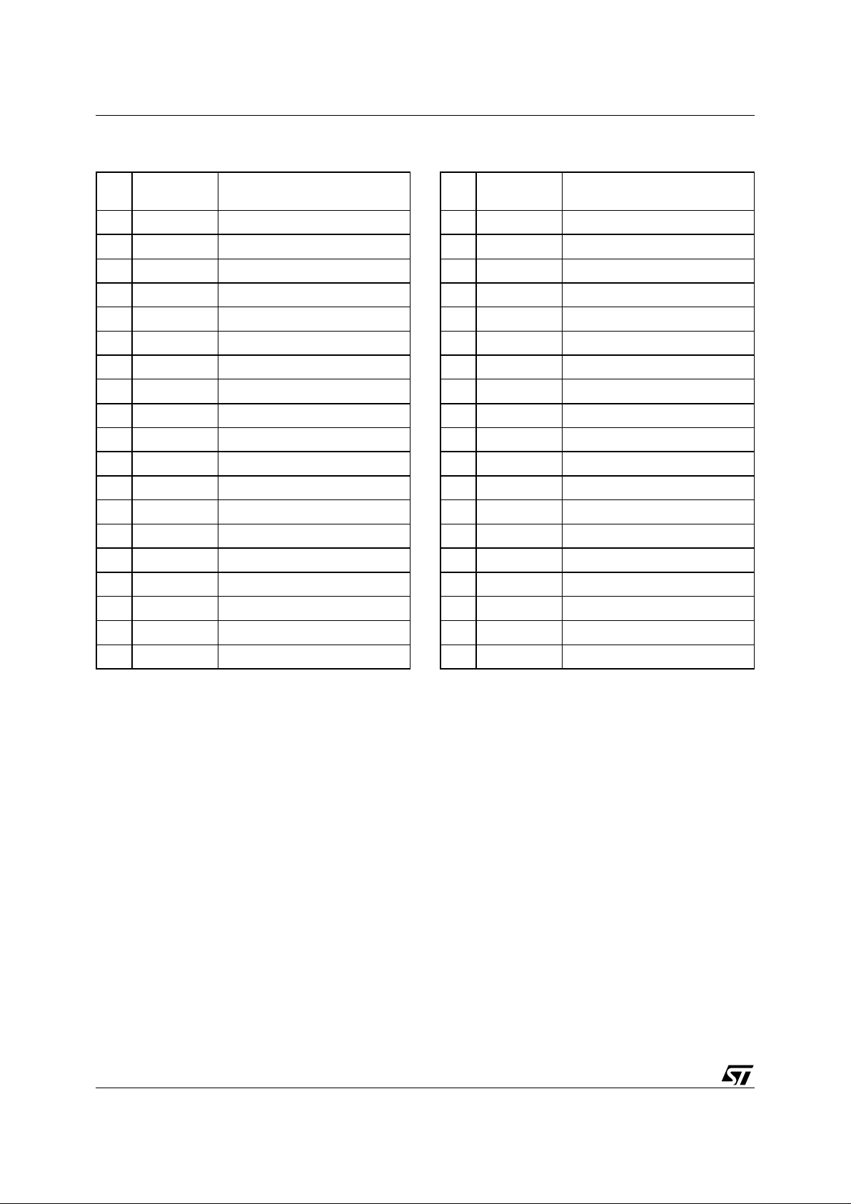
Table 3. Top Boot Block Addresses,
M29W008AT
#
Size
(Kbytes)
Address Range
18 16 FC000h-FFFFFh
17 8 FA000h-FBFFFh
16 8 F8000h-F9FFFh
15 32 F0000h-F7FFFh
14 64 E0000h-EFFFFh
13 64 D0000h-DFFFFh
12 64 C0000h-CFFFFh
11 64 B0000h-BFFFFh
10 64 A0000h-AFFFFh
9 64 90000h-9FFFFh
8 64 80000h-8FFFFh
7 64 70000h-7FFFFh
6 64 60000h-6FFFFh
5 64 50000h-5FFFFh
4 64 40000h-4FFFFh
3 64 30000h-3FFFFh
2 64 20000h-2FFFFh
1 64 10000h-1FFFFh
0 64 00000h-0FFFFh
Table 4. Bottom Boot Block Addresses,
M29W008AB
#
Size
(Kbytes)
Address Range
18 64 F0000h-FFFFFh
17 64 E0000h-EFFFFh
16 64 D0000h-DFFFFh
15 64 C0000h-CFFFFh
14 64 B0000h-BFFFFh
13 64 A0000h-AFFFFh
12 64 90000h-9FFFFh
11 64 80000h-8FFFFh
10 64 70000h-7FFFFh
9 64 60000h-6FFFFh
8 64 50000h-5FFFFh
7 64 40000h-4FFFFh
6 64 30000h-3FFFFh
5 64 20000h-2FFFFh
4 64 10000h-1FFFFh
3 32 08000h-0FFFFh
2 8 06000h-07FFFh
1 8 04000h-05FFFh
0 16 00000h-03FFFh

5/30
M29W008AT, M29W008AB
SIGNAL DESCRIPTIONS
See Figure 1 and Table 1.
Address Inputs (A0-A19). The address inputs
for the memory array are latched during a write operation on the falling edge of Chip Enable E
or
Write Enable W
. When A9 is raised to VID, either a
Read Electronic Signature Manufacturer or Device
Code, Block Protection Status or a Write Block
Protection or Block Unprotection is enabled depending on the combinat ion of levels on A0, A1
A6, A12 and A15.
Data Input/Outputs (DQ0-DQ7). The input is
data to be programm ed in the memory array or a
command to be written to the C.I. Both are latched
on the rising edge of Chip Enable E or Write E nable W
. The output is data from the Memory Array,
the Electronic Signature Manufa cturer or Device
codes, the Block Prote ction Status or the Status
register Data Polling bit DQ7, the Toggle Bits DQ6
and DQ2, the Error bit DQ5 or the Erase Timer bit
DQ3. Outputs are valid when Chip Enable E
and
Output Enable G
are active. The output is high i mpedance when the chip is deselected or the outputs are disabled and when RP
is at a Low level.
Chip Enable (E
). The Chip Enable input acti-
vates the memory control logic, input buffers, decoders and sense amplifiers. E
High deselects the
memory and reduces the power consumption to
the stand-by level. E
can also b e used to control
writing to the command register and to the memory array, while W
remains at a low le v el. The Chip
Enable must be forced to V
ID
during the Block Un-
protection operation.
Output Enable (G
). The Output Enable gates the
outputs through the data buffers during a read operation. When G
is High the outpu ts are High im-
pedance. G
must be forced to VID level during
Block Protection and Unprotection operations.
Write Enable (W
). This input controls writing to
the Command Register and Address and Data
latches.
Ready/Busy Output (RB
). Ready/Busy is an
open-drain output and gives the internal state of
the P/E.C. of the device. When RB
is Low, the device is Busy with a Program or Erase operation
and it will not accept any additional program or
erase instructions except the Erase Suspend instruction.
When RB
is High, the device is ready for any
Read, Program or Erase operation. The RB
will
also be High when the memory is put in Erase
Suspend or Stand-by modes.
Reset/Block Temporary Unprotect Input (RP
).
The RP
Input provides hardware reset and protected block(s) temporary unprotection functions.
Reset of the memory is achieved by pulling RP
to
V
IL
for at least t
PLPX
. When the reset pulse is given, if the memory is in Read or Stand-by modes, it
will be available for new operations in t
PHEL
after
the rising edge of RP
.
If the memory is in Erase, Erase Suspend or Program modes the reset will take t
PLYH
during which
the R B
signal will be held at VIL. The end of the
memory re set will be indicate d by the risi ng edge
of RB
. A hardware reset d uring an Erase or Program operation will corrupt the data being programmed or the sector(s) being erased. See
Tables 15, 16 and Figure 8.
Temporary block unprotection is made by holding
RP
at VID. In this condi tion previously pro tected
blocks can be programmed or erased. The transition o f RP
from VIH to VID must slower than t
PH-
PHH
. (See Tables 17, 18 and Figure 8). When RP
is returned from VID to VIH all blocks temporarily
unprotected will be again protected.
V
CC
Supply Voltage. The power supply for all
operations (Read, Program and Erase).
V
SS
Ground. VSS is the reference for all voltage
measurements.

M29W008AT, M29W008AB
6/30
DEVICE OPERATIONS
See Tables 5, 6 and 7.
Read. Read operations are used to output the
contents of the Memory Array, the Electronic Signature, the Status Register or the Block Protection
Status. Both Chip Enab le E
and Output Enable G
must be low in order to read the output of the memory. A new read operation is initiated either on the
falling edge of Chip, Enable E
, or on any address
transition with E
at VIL.
Write. Write operations are used to give I nstruction Commands to the memory or to latch input
data to be programmed. A write operation is initiated when Chip Enable E
is Low and Write Enable
W
is Low with Output E nable G High. Addresses
are latched on the falling edge of W
or E whichever
occurs last. Commands and Input Data are
latched on the rising edge of W
or E whichever oc-
curs first.
Output Disa bl e . The data outputs are high im-
pedance when the Output Enable G
is High with
Write Enable W
High.
Stand-by. The memory is in stand-by wh en Chip
Enable E
is High and the P/E.C. is idle. The power
consumption is reduced to the st and-by level and
the outputs are high impedanc e, independent of
the Output Enable G
or Write Enable W inputs.
Automatic Stand-by. After 150ns of bus inactivity (no address transition, E
= VIL) and when CMOS
levels are driving the addresses, the chip automatically enters a pseudo-stand-by mode where consumption is reduced to the CMOS stand-by value,
while outpu t s still d riv e th e bu s (if G
= VIL).
Electronic Signature. Tw o codes identifying the
manufacturer and the device can be read from the
memory. The manufacturer’s code for STMicroelectronics is 20h, the device code is D2h for the
M29W008AT (Top Boot) and DCh for the
M29W008AB (Bottom Boot). These codes allow
programming equipment or applications to automatically match their interface to the characteristics of the M29W008A. The Electronic Signature is
output by a Read operation when the voltage applied to A9 is at V
ID
and address inputs A1 is Low.
The manufacturer code is output when the Address input A0 is Low a nd the device code when
this input is High. Other Address inputs are ignored. The Electronic Signature can also be read,
without raising A9 to V
ID
, by giving the memory the
Instructi on AS.
Block Protection. Each block c an be separately
protected against Program or Erase on program ming equipment. Block protection provid es additional data security, as it disables all program or
erase operations. This mode is activated when
both A9 and G
are raised to VID and an address in
the block is applied on A13-A1 9. Block protection
is initiated on the edge of W
falling to VIL. Then af-
ter a delay of 100µs, the edge of W
rising to V
IH
ends the protection operations. Block protection
verify is achieved by bringing G
, E, A0 a nd A6 t o
V
IL
and A1 to VIH, while W is at VIH and A9 at VID.
Under these conditions, reading the data output
will yield 01h if the block def ined by the inputs on
A13-A19 is protected. Any at tempt to program or
erase a protected block will be ignored by the device .
Block Temporary Unprotection. Any previously
protected block can be temporaril y unprotec ted in
order to change stored data. The tem porary unprotection mode is activated by bringing RP to VID.
During the temporary unprotection mode the previously protected blocks a re unprotected. A block
can be selected and data can be modified by executing the Erase or Program instruction with the
RP
signal held at VID. When RP is returned to VIH,
all the previously protected blocks are again protected.
Block Unprotection. All protected blocks can be
unprotected on programming equ ipment to allow
updating of bit contents. All blocks must first be
protected before the unprotection operation. Block
unprotection is activated when A9, G
and E are at
V
ID
and A12, A15 at VIH. Unprote ction is init iated
by the edge of W
falling t o VIL. After a delay of
10ms, the unprotection operation will end. Unprotection verify is achieved by bringing G
and E to
V
IL
while A0 is at VIL, A6 and A1 are at VIH and A9
remains at V
ID
. In these conditions, reading the
output data will yield 00h if the block defined by the
inputs A13-A19 has been s uccessfully unprotected. Each block must be separately verified by giving its address in order to ensure that it has been
unprotected.
7/30
M29W008AT, M29W008AB
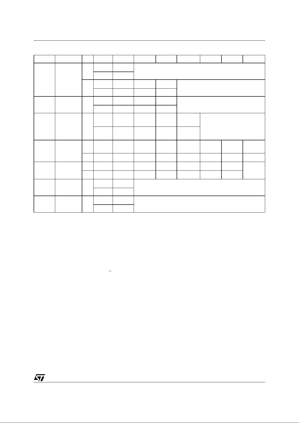
Table 5. User Bus Operations
(1)
Note: 1. X = VIL or VIH.
2. Block Address m ust be given an A13-A19 bi ts.
3. See Table 7.
4. Oper atio n pe rform ed on pro g ramming equipment.
Table 6. Read Electronic Signature (following AS instruction or with A9 = VID)
Table 7. Read Block Protection with AS Instruction
Operation E G W RP A0 A1 A6 A9 A12 A15 DQ0-DQ7
Read Byte
V
IL
V
IL
V
IH
V
IH
A0 A1 A6 A9 A12 A15 Data Output
Write Byte
V
IL
V
IH
V
IL
V
IH
A0 A1 A6 A9 A12 A15 Data Input
Output Disable
V
IL
V
IH
V
IH
V
IH
XXXXXX Hi-Z
Stand-by
V
IH
XX
V
IH
XXXXXX Hi-Z
Reset X X X
V
IL
XXXXXX Hi-Z
Block
Protection
(2,4)
V
IL
V
ID
VIL Pulse V
IH
XXX
V
ID
XX X
Blocks
Unprotection
(4)
V
ID
V
ID
VIL Pulse V
IH
XXX
V
ID
V
IH
V
IH
X
Block
Protection
Verify
(2,4)
V
IL
V
IL
V
IH
V
IH
V
IL
V
IH
V
IL
V
ID
A12 A15
Block
Protect
Status
(3)
Block
Unprotection
Verify
(2,4)
V
IL
V
IL
V
IH
V
IH
V
IL
V
IH
V
IH
V
ID
A12 A15
Block
Protect
Status
(3)
Block
Temporary
Unprotection
XX X
V
ID
XXXXXX X
Code Device E
G W A0 A1
Other
Addresses
DQ0-DQ7
Manufact. Code
V
IL
V
IL
V
IH
V
IL
V
IL
Don’t Care 20h
Code E
G W A0 A1 A13-A19
Other
Addresses
DQ0-DQ7
Protected Block
V
IL
V
IL
V
IH
V
IL
V
IH
Block Address Don’t Care 01h
Unprotected Block
V
IL
V
IL
V
IH
V
IL
V
IH
Block Address Don’t Care 00h
M29W008AT, M29W008AB
8/30
Table 8. Commands
Hex Code Command
00h Invalid/Reserved
10h Chip Erase Confir m
20h Rese r ved
30h Block Erase Resume/Confirm
80h Set-up Erase
90h
Read Electronic Signature/
Block Protection Status
A0h Program
B0h Erase Suspend
F0h Read Array/Reset
INSTRUCTIONS AND COMMANDS
The Command Interface latches c ommands written to the memory. Instructions are made up from
one or more commands to perform Read Memory
Array, Read Electronic Signature, Read Block Protection, Program, Block Erase, Chip E rase, Eras e
Suspend and Erase Resume. Commands are
made of address and data sequences. The instructions require from 1 to 6 cycles, the first or first
three of which are always write operations used to
initiate the instruction. They are followed by either
further write cycles to confirm the first command or
execute the command immediately. Command sequencing must be followed exactly. Any invalid
combination of commands will reset the device to
Read Array. The increase d number of cycles has
been chosen to assure maximum data security. Instructions are initialised by two initial Coded cycles
which unlock the Command Interface. In addition,
for Erase, instruction confirmation is again preceded by the two Coded cycles.
Status Register Bits
P/E.C. status is indicated during execution by Data
Polling on D Q7, detection of T oggle on DQ6 and
DQ2, or Error on DQ5 and E ras e T imer DQ3 bits.
Any read attempt during P rogram or Erase command execution will automatically output these
five Status Register bits. The P/E.C. automatically
sets bits DQ2, DQ 3, DQ5, DQ6 and DQ7. Other
bits (DQ0, DQ1 and D Q4) a re reserved for future
use and should be masked. See Tables 10 and 11.
Data Polling Bit (DQ7). When Program ming operations are in progress, this bit out puts the complement of the bit being programmed on DQ7.
During Erase operation, it outputs a ’0’. After completion of the operation, DQ7 will output the bit last
program me d or a ’1 ’ after er asi ng. Data Pollin g is
valid and only effective during P/E.C. operation,
that is after the fourth W
pulse for programming or
after the sixth W
pulse for erase. It must be performed at the address being programmed or at an
address within the block being erased. If all the
blocks selected for erasure are protected, DQ7 will
be set to '0' for about 100µs, and then return to the
previous addressed memory data value. See Figure 10 for the D ata P olling flowcha rt a nd F igure 9
for the Data Polling waveforms. DQ7 will also flag
the Erase Suspend mode by switching from '0' to
'1' at the start of the Erase Suspend. In order to
monitor DQ7 in t he Erase Sus pend mode an address within a block being erased must be provided. For a Read Operation in Erase Suspend
mode, DQ7 will output '1' if the read is attempted
on a block being erased and the data value on other blocks. During Program operation in Erase Suspend Mode, DQ7 will have the same behavior as
in the normal program execution outside of the
suspend mode.
Toggle Bit (DQ6). When Programming or Erasing operations are in progress, successive attempts to read DQ6 will output complementary
data. DQ6 will toggle following toggling of either G
,
or E
when G is low. The operation is completed
when two successive reads yield the same output
data. The next read will output the bit last programmed or a '1' after erasing. The toggle bit DQ6
is valid only during P/E.C. op erations, that is after
the fourth W
pulse for programming or after the
sixth W
pulse for Erase. If the blocks selected for
erasure are protected, DQ6 will toggle for about
100µs and then return ba ck to Read. DQ6 will be
set to '1' if a Read operation is at tempted on an
Erase Suspend block. When erase is suspended
DQ6 will toggle during programming operations in
a block different to the block in Erase Suspend. Either E
or G toggling will cause DQ6 to toggle. See
Figure 11 for Toggle Bit flowchart and Figure 12
for Toggle Bit wav e f o r m s .
9/30
M29W008AT, M29W008AB
Table 9. Instructions
(1)
Note: 1. Commands not interpreted in this table will default to read array mode.
2. A wait of t
PLYH
is necessary after a Read/Reset command if the memory was in an Erase or Program mode before starting any new
operation (see Tables 15, 16 and Figur e 9).
3. X = Don’t Car e.
4. The f i rst cycle s of the RD or AS instruction s are follo wed by read operati ons. Any number of read cycles can occ ur after the command cycl e s.
5. Signature Addr ess bits A0, A 1, a t V
IL
will output Manufacturer code (20h). Address bits A0 at VIH and A1, at VIL will out put De vice
code.
6. Block Protect io n Address: A 0, at V
IL
, A1 at VIH and A13-A19 within the Block will output the Block Protection status.
7. For C oded cycles address inputs A15-A 19 are don’t care.
8. Opti onal, additional Blocks addr esses mus t be entered within the erase t i meout delay a ft er las t write entry, t i meout st atusc a n b e
verified through DQ3 value (see Erase Timer Bit DQ3 description). When full command is entered, read Data Polling or Toggle bit
until Erase is completed or suspended.
9. Rea d Data Poll i ng, T oggle bits or RB
until Erase complete s.
10. Duri ng Erase Su spend, Read and Data Prog ram functions are allow ed in blocks not bei ng erased.
Mne. Instr. Cyc. 1st Cyc. 2nd Cyc. 3rd Cyc. 4th Cyc. 5th Cyc. 6th Cyc. 7th Cyc.
RD
(2,4)
Read/Reset
Memory Array
1+
Addr.
(3,7)
X
Read Memo ry Array unti l a new write cycle is initi ated.
Data F0h
3+
Addr.
(3,7)
555h 2AAh 555h
Read Memory Array until a new write cycle is
initiated.
Data AAh 55h F0h
AS
(4)
Auto Select 3+
Addr.
(3,7)
555h 2AAh 555h
Read Ele ct ronic Signature or Block P rotection
Status until a new write cycle is initiated. See Note 5
and 6.Data AAh 55h 90h
PG Pr ogram 4
Addr.
(3,7)
555h 2AAh 555h
Program
Address
Read Data Polling or Toggle Bit until
Program com pl etes.
Data AAh 55h A0h
Program
Data
BE Block Erase
6
Addr.
(3,7)
555h 2AAh 555h 555h 2AAh
Block
Address
Additional
Block
(8)
Data AAh 55h 80h AAh 55h 30h 30h
CE Chip Erase
6
Addr.
(3,7)
555h 2AAh 555h 555h 2AAh 555h
Note 9
Data AAh 55h 80h AAh 55h 10h
ES
(10)
Eras e Suspen d 1
Addr.
(3,7)
X
Read until Toggle stops, then read all th e data needed from any Block( s) not
being erased then Resum e Erase.
Data B0h
ER Erase Resume 1
Addr.
(3,7)
X
Read Data Polling or Toggle Bits until Erase completes or Erase is suspended
another time.
Data 30h
 Loading...