

SGS Thomson Microelectronics M29W004B, M29W004T Datasheet
Low Voltage Single Supply Flash Memory
M29W004T and M29W004B are replaced
respectively by the M29W004BT and
M29W004BB
2.7 to 3.6V SUPPLY VOLTAGE for
PROGRAM, ERASE and READ OPERATIONS
FAST A CCES S TIME : 100ns
FAST PROGRAMMING TIME: 10µs typical
PROGRAM/ERASE CONTROLLER (P/E.C.)
– Program Byte-by-Byte
– Status Register bits and Ready/Busy Output
MEMOR Y BLOCKS
– Boot Block (Top or Bottom location)
– Parameter and Main blocks
BLOCK, MULTI-BLOCK and CHIP ERASE
MULTI BLOCK PROTECTION/TEMPORARY
UNPROTECTION MODES
ERASE SUSPEND and RESUME MOD ES
– Read and Program another Block during
Erase Suspend
LOW POWER CONSUMPTION
– Stand-by and Automatic Stand-by
100,000 PROGRAM/ERASE CYCLES per
BLOCK
20 YEARS DA TA RETE NT ION
– Defectivity below 1ppm/year
ELECTRONIC SIGNATURE
– Manufacturer Code: 20h
– Device Code, M29W004T: EAh
– Device Code, M29W004B: EBh
DESCRIPTION
The M29W004 is a non-volatile memory that may
be erased electrically at the block or chip level and
programmed in-system on a Byte-by-Byte basis
using only a single 2.7V to 3.6V V
Program and Erase operations the necessary high
voltages are generated internally. The device can
also be programmed in standard programmers.
The array matrix organisation allows each block to
be erased and reprogrammed without affecting
other blocks. Blocks can be protected against programing and erase on programming equipment,
and temporarily unprotected to make changes in
supply. For
CC
M29W004T
M29W004B
4 Mbit (512Kb x8, Boot Block)
NOT FOR NEW DESIGN
TSOP40 (N)
10 x 20 mm
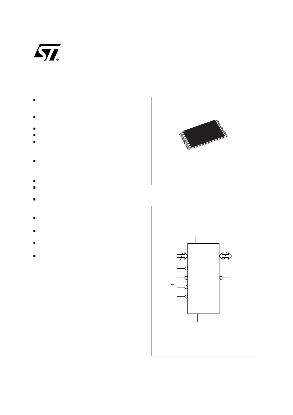
Figure 1. Logic Diagram
V
CC
A0-A18
W
RP
19
E
G
M29W004T
M29W004B
V
SS
8
DQ0-DQ7
RB
AI02063
June 1999 1/30
This is information on a product still in production but not recommended for new designs.
M29W004T, M29W004B
Figure 2. TSOP Pin Connections
A16
A15
A14
A13
A12
A11
A9
A8
W
RP
NC
RB
A18
A6
A5
A4
A3
A2
A1
Warning:
NC = Not Connected.
DESCRIPTION
1
M29W004T
10
M29W004B
11
20 21
AI02064
(Cont’d)
40
31
30
A17
V
SS
NC
NC
A10
DQ7
DQ6
DQ5
DQ4
V
CC
V
CC
NC
DQ3
DQ2A7
DQ1
DQ0
G
V
SS
E
A0
the application. Each block can be programmed
and erased over 100,000 cycles.
Instructions for Read/Reset, Auto Select for reading the Electronic Signature or Block Protection
status, Programming, Block and Chip Erase, Erase
Suspend and Resume are written t o the device in
Tabl e 1. Signal Names
A0-A18 Address Inputs
DQ0-DQ7 Data Input/Outputs, Command Inputs
E Chip Enable
G Output Enable
W Write Enable
RP Reset / Block Temporary Unprotect
B Ready/Busy Output
R
V
CC
V
SS
Supply Voltage
Ground
cycles of commands to a Command Interface using
standard microprocessor write timings.
The device is offered in TSOP40 (10 x 20mm)
package.
Organisation
The M29W004 is organised as 512K x8. The memory uses the address inputs A0-A18 and the Data
Input/Outputs DQ0-DQ7. Memory control is provided by Chip Enable
Enable
W inputs.
A Reset/Block T emporary Unprotection
E, Output Enable G and Write
RP tri-level
input provides a hardware reset when pulled Low,
and when held High (at V
) temporarily unprotects
ID
blocks previously protected allowing them to be
programed and erased. Erase and Program operations are controlled by an internal Program/Erase
Controller (P/E.C.). Status Register data output on
DQ7 provides a Data Polling signal, and DQ6 and
DQ2 provide Toggle signals to indicate the state of
the P/E.C operations. A Ready/Busy R
B output
indicates the completion of the internal algorithms.
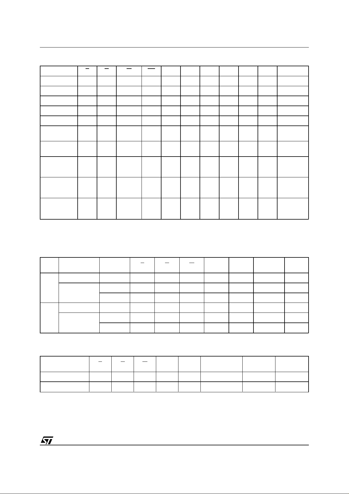
T ab le 2. Absolute Maximum Ratings
Symbol Parameter Value Unit
T
A
T
BIAS
T
STG
(2)
V
IO
V
CC
V
(A9, E, G, RP)
Notes:
1. Except for the rating "Operating Temperature Range", stresses above those listed in the Table "Absolute Maximum Ratings"
may cause permanent damage to the device. These are stress rating s only and operation of the device at these or any other
conditions above those indicated in the Operating sections of this specification is not implied. Exposure to Absolute Maximum
Rating conditions for extended periods may affect device reliability. Refer also to the STMicroelectronics SURE Program and other
relevant quality documents.
2. Minimum Voltage may undershoot to –2V during transition and for less than 20ns.
3. Depends on range.
2/30
Ambient Operating Temperature
Temperature Under Bias –50 to 125
Storage Temperature –65 to 150
Input or Output Voltages –0.6 to 5 V
Supply Voltage –0.6 to 5 V
(2)
A9, E, G, RP Voltage –0.6 to 13.5 V
(1)
(3)
–40 to 85
C
°
C
°
C
°

M29W004T, M29W004B
Memory Blocks
The devices feature asymmetrically blocked architecture providing system memory integration. Both
M29W004T and M29W004B devices have an array
of 11 blocks, one Boot Block of 16K Bytes, two
Parameter Blocks of 8K Bytes, one Main Block of
32K Bytes and seven Main Blocks of 64K Bytes.
The M29W004T has the Boot Block at the top of
the memory address space and the M29W004B
locates the Boot Block starting at the bottom. The
memory maps are showed in Figure 3. E ach block
can be erased separately, any combination of
blocks can be specified for multi-block erase or the
entire chip may be erased. The Erase operations
are managed automatically by the P/E.C. The block
erase operation can be suspended in order to read
from or program to any block not being ersased,
and then resumed.
Block protection provides additional data security.
Each block can be separately protected or unprotected against Program or Erase on programming
equipment. All previously protected blocks can be
temporarily unprotected in the application.
Bus Operations
The following operations can be performed usi ng
the appropriate bus cycles: Read (Array , E lectronic
Signature, Block Protection Status), Write command, Output Disable, Standby, Reset, Block Protection, Unprotection, Protection Verify,
Unprotection Verify and Blo ck Temporary Unprotection. See Tables 4 and 5.
Command Interface
Instructions, made up of commands written in cycles, can be given to the Program/Erase Controller
through a Command Interface (C.I.). For added
data protection, program or erase execution starts
after 4 or 6 cycles. The first, second, fourth and fifth
cycles are used to input Coded cycles to the C.I.
This Coded sequence is the same for all Program/Erase Controller instructions. The ’Command’ itself and its confirmation, when applicable,
are given on the third, four th or sixth cycles. Any
incorrect command or any improper command sequence will reset the device to Read Array mode.
Instructions
Seven instructions are defined to perform Read
Array , Auto Select (to read the Electronic Signature
or Block Protection Status), Program, Block Erase,
Chip Erase, Erase Suspend and Er ase Resume.
The internal P/E.C. automatically handles all timing and verification of the Program and Erase
operations. The Status Register Data Polling, Toggle, Error bits and the R
B output may be read at
any time, during programming or erase, to monitor
the progress of the operation.
Instructions are composed of up to six cycles. The
first two cycles input a Coded sequence to the
Command Interface which is common to all instructions (see Table 8). The third cycle inputs the
instruction set-up command. Subsequent cycles
output the addressed data, Electronic Signature or
Block Protection Status for Read operations. In
order to give additional data protection, the instructions for Program and Block or Chip Erase require
further command inputs. For a P rogram instruction,
the fourth command cycle inputs the address and
data to be programmed. For an Erase instruction
(Block or Chip), the fourth and fifth cycles input a
further Coded sequence before the Erase confirm
command on the sixth cycle. Erasure of a memory
block may be suspended, in order to read data from
another block or to program data in another block,
and then resumed.
When power is first applied or if Vcc falls below
, the command interface is reset to Read
V
LKO
Array.
SIGNAL DESCRIP TIONS
See Figure 1 and T able 1.
Address Inputs (A0-A18)
. The address inputs for
the memory array are latched during a write operation on the falling edge of Chip E nable
Enable
W. In Word-wide organisation the address
lines are A0-A18. When A9 is raised to V
E or Write
, either
ID
a Read Electronic Signature Manufacturer or Device Code, Block Protection Status or a Write Block
Protection or Block Unprotection is enabled depending on the combination of levels on A0, A1, A6,
A12 and A15.
Data Input/Outputs (DQ0-DQ7).
The input is data
to be programmed in the memory arr ay or a command to be written to t he C.I. Both are latched on
the rising edge of Chip Enable
E or Write Enable
W. The output is data from the Memory Array, the
Electronic Signature Manufacturer or Device
codes, the Block Protection Status or the Status
register Data Polling bit DQ7, the Toggle Bits DQ6
and DQ2, the Error bit DQ5 or the Erase Timer bit
DQ3. Outputs are valid when Chip Enable
Output Enable
G are active. The output is high
E and
impedance when the chip is deselected or the
outputs are disabled and when
Chip Enable (
The Chip Enable input activates
E).
RP is at a Low level.
the memory control logic, input buffers, dec oders
and sense amplifiers.
E High deselects the memory
and reduces the power consumption to the standby
level.
E can also be used to control writing to the
command register and to the memory array, while
W remains at a low level. The Chip Enable must be
forced to V
during the Block Unprotection opera-
ID
tion.
3/30
M29W004T, M29W004B
Figure 3. Memory Map and Block Address Table (x8)
7FFFFh
7C000h
7BFFFh
7A000h
79FFFh
78000h
77FFFh
70000h
6FFFFh
60000h
5FFFFh
50000h
4FFFFh
40000h
3FFFFh
30000h
2FFFFh
20000h
1FFFFh
10000h
0FFFFh
00000h
M29W004T
16K BOOT BLOCK
8K PARAMETER BLOCK
8K PARAMETER BLOCK
32K MAIN BLOCK
64K MAIN BLOCK
64K MAIN BLOCK
64K MAIN BLOCK
64K MAIN BLOCK
64K MAIN BLOCK
64K MAIN BLOCK
64K MAIN BLOCK
7FFFFh
70000h
6FFFFh
60000h
5FFFFh
50000h
4FFFFh
40000h
3FFFFh
30000h
2FFFFh
20000h
1FFFFh
10000h
0FFFFh
08000h
07FFFh
06000h
05FFFh
04000h
03FFFh
00000h
M29W004B
64K MAIN BLOCK
64K MAIN BLOCK
64K MAIN BLOCK
64K MAIN BLOCK
64K MAIN BLOCK
64K MAIN BLOCK
64K MAIN BLOCK
32K MAIN BLOCK
8K PARAMETER BLOCK
8K PARAMETER BLOCK
16K BOOT BLOCK
AI02093
Output Enable (
The Output Enable gates the
G).
outputs through the data buffers during a read
operation. When
impedance.
G is High the outputs are High
G must be forced to VID level during
Block Protection and Unprotection operations.
Write Enable (
This input controls writing to the
W).
Command Register and Address and Data latches.
Ready/Busy Output (R
Ready/Busy is an
B).
open-drain output and gives the internal state of the
P/E.C. of the device. When R
B is Low, the device
is Busy with a Program or Erase operation and it
will not accept any additional program or erase
instructions except the Erase Suspend instruction.
When R
Program or Erase operation. The R
B is High, the device is ready for any Read,
B will also be
High when the memory is put in E ras e S uspend or
Standby modes.
Reset/Block Temporary Unprotect Input (
The
RP Input provides hardware reset and pro-
RP).
tected block(s) temporary unprotection functions.
Reset of the memory is acheived by pulling
for at least t
V
IL
4/30
. When the reset pulse is given,
PLPX
RP to
if the memory is in Read or Standby modes, it will
be available for new operations in t
rising edge of
RP. If the memory is in Erase, Erase
PHEL
after the
Suspend or Program modes the reset will take
t
during which the RB signal will be held at VIL.
PLYH
The end of the memory reset will be indicated by
the rising edge of R
B. A hardware reset during an
Erase or Program operation will corrupt the data
being programmed or the sec tor(s) being era sed.
See Table 14 and Figure 9.
Temporary block unprotection is made by holding
RP at VID. In this condition previously protected
blocks can be programmed or erased. The transi-
RP from VIH to VID must slower than t
tion of
When
RP is returned from VID to VIH all blocks
PHPHH
temporarily unprotected will be again protected.
See Table 15 and Figure 9.
Supply Voltage.
V
CC
The power supply for all
operations (Read, Program and Erase).
is the reference for all voltage
Ground.
V
SS
V
SS
measurements.
.
M29W004T, M29W004B
T ab le 3A. M29W004T Block Address Table
Address Range A18 A17 A16 A15 A14 A13
00000h-0FFFFh 0 0 0 X X X
10000h-1FFFFh 0 0 1 X X X
20000h-2FFFFh 0 1 0 X X X
30000h-3FFFFh 0 1 1 X X X
40000h-4FFFFh 1 0 0 X X X
50000h-5FFFFh 1 0 1 X X X
60000h-6FFFFh 1 1 0 X X X
70000h-77FFFh 1110XX
78000h-79FFFh 111100
7A000h-7BFFFh 111101
7C000h-7FFFFh 11111X
T ab le 3B. M29W004B Block Address Table
Address Range A18 A17 A16 A15 A14 A13
00000h-03FFFh 00000X
04000h-05FFFh 000010
06000h-07FFFh 000011
08000h-0FFFFh 0001XX
10000h-1FFFFh 0 0 1 X X X
20000h-2FFFFh 0 1 0 X X X
30000h-3FFFFh 0 1 1 X X X
40000h-4FFFFh 1 0 0 X X X
50000h-5FFFFh 1 0 1 X X X
60000h-6FFFFh 1 1 0 X X X
70000h-7FFFFh 1 1 1 X X X
5/30

M29W004T, M29W004B
DEVICE O PERATIONS
See Tables 4, 5 and 6.
Read operations are used to output the
Read.
contents of the Memory Array, the Electronic Signature, the Status Register or the Block Protection
Status. Both Chip Enable
E and Output Enable G
must be low in order to read the output of the
memory.
Write operations are used to give Instruction
Write.
Commands to the memory or to latch input data to
be programmed. A write operation is initiated when
Chip Enable
with Output Enable
on the falling edge of
E is Low and Write Enable W is Low
G High. Addresses are latched
W or E whichever occurs last.
Commands and Input Data are latched on the rising
edge of
Output Disable.
ance when the Output Enable
Enable
Standby.
Enable
W or E whichever occurs first.
The data outputs are high imped-
G is High with Write
W High.
The memory is in standby when Chip
E is High and the P/E .C. is idle. T he power
consumption is reduced to the standby level and
the outputs are high impedance, independent of
the Output Enable
Automatic Standby.
G or Write Enable W inputs.
After 150ns of bus inactivity
and when CMOS levels are driving the addresses,
the chip automatically enters a pseudo-standby
mode where consumption is reduced to the CMOS
standby value, while outputs still drive the bus.
Electronic S ignature.
Two codes identifying the
manufacturer and the device can be read from the
memory. The manufacturer’s code for STMicroelectronics is 20h, the device code is EAh for
the M29W004T (Top Boot) and EBh for the
M29W004B (Bottom Boot). These codes allow programming equipment or applications to aut omatically match their interface to the characteristics of
the M29W004. The Electronic Signature is output
by a Read operation when the voltage applied to
A9 is at V
and address input A1 is Low. The
ID
manufacturer code is output when the Address
input A0 is Low and the device code when this
input is High. Other Address inputs are ignored.
The Electronic Signature can also be read, without
raising A9 to V
, by giving the m emory the Ins truc-
ID
tion AS.
Block Protection.
Each block can be separately
protected against Program or Erase on programming equipment. Block protection provides additional data security, as it disables all program or
erase operations. This mode is activated when both
A9 and
G are raised to VID and an address in the
block is applied on A13-A18. The Block Protection
algorithm is shown in Figure 14. Block protection is
initiated on the edge of
a delay of 100µs, the edge of
W falling to VIL. Then after
W rising to VIH ends
the protection operations. Block protection verify is
achieved by bringing
, while W is at VIH and A9 at VID. Under these
to V
IH
G, E, A0 and A6 to VIL and A1
conditions, reading the data output will yield 01h if
the block defined by the inputs on A13-A18 is
protected. Any attempt to program or erase a protected block will be ignored by the device.
Block Temporary Unprotection.
Any previously
protected block can be temporarily unprot ected in
order to change stored data. The temporary unprotection mode is activated by bringing
RP to VID.
During the temporary unprotection mode the previously protected blocks are unprotected. A block
can be selected and data can be modified by
executing the Erase or Program instruction with the
RP signal held at VID. When RP is returned to VIH,
all the previously protected blocks are again protected.
Block Unprotection.
All protected blocks can be
unprotected on programming equipment to allow
updating of bit contents. All blocks must first be
protected before the unprotection operation. Block
unprotection is activated when A9,
and A12, A15 at VIH. The Block Unprotection
V
ID
G and E are at
algorithm is shown in Figure 15. Unprotection is
initiated by the edge of
W falling to VIL. After a delay
of 10ms, the unprotection operation will end. Unprotection verify is achieved by bringing
while A0 is at VIL, A6 and A1 are at VIH and A9
V
IL
remains at V
. In these conditions, reading the
ID
G and E to
output data will yield 00h if the block defined by the
inputs A13-A18 has been succesfully unprotected.
Each block must be separately ver ified by giving its
address in order to ensure that it has been unprotected.
6/30
M29W004T, M29W004B
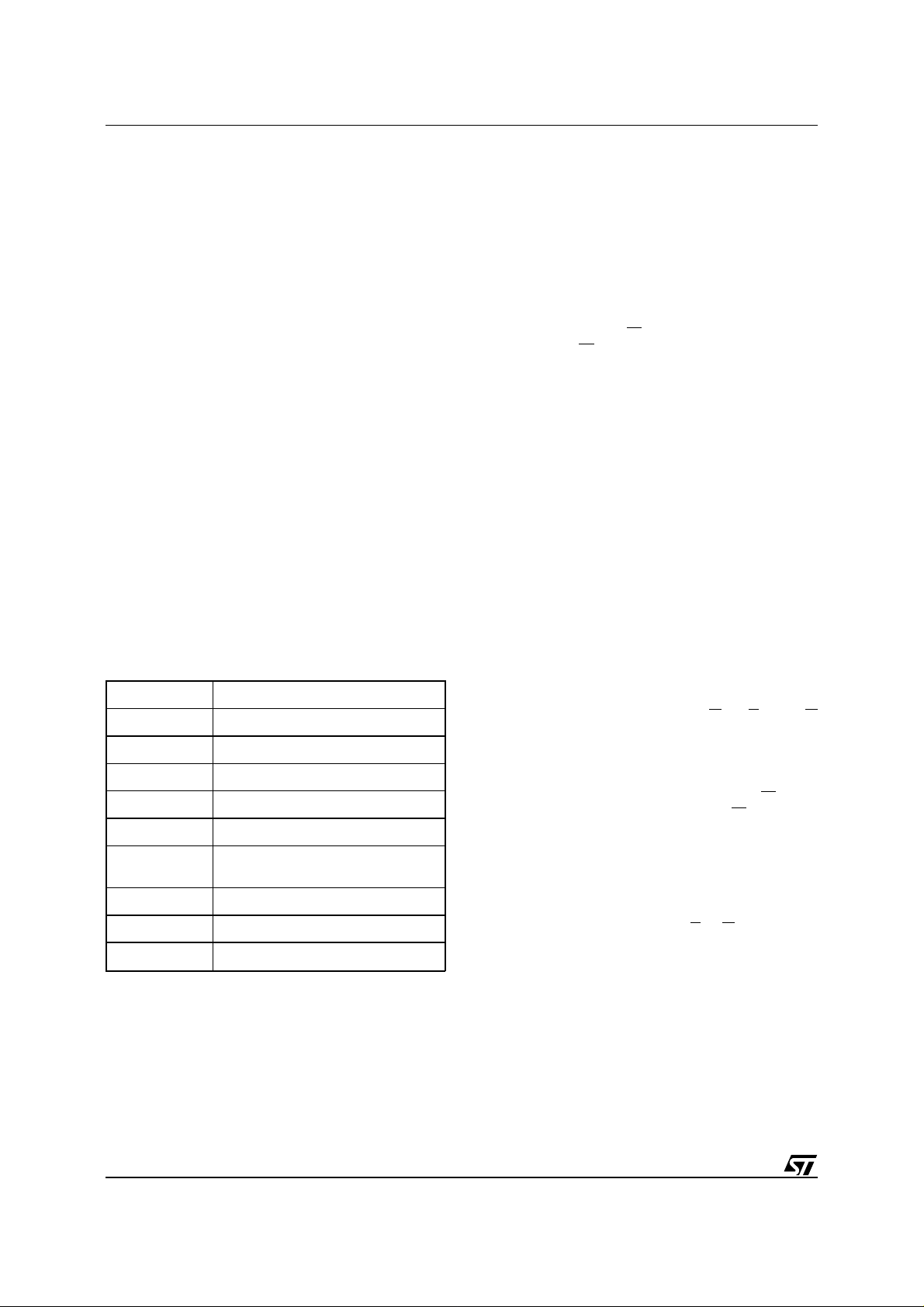
T ab le 4. User Bus Operations
(1)
Operation E G W RP A0 A1 A6 A9 A12 A15 DQ0-DQ7
Read Byte V
Write Byte V
Output Disable V
Standby V
Reset X X X V
Block
Protection
(2,4)
Blocks
Unprotection
VIL VIDVIL Pulse V
V
(4)
V
IL
IL
IL
IH
ID
IL
V
IH
V
IH
XXVIHXXXXXX Hi-Z
V
ID
V
IH
V
IL
V
IH
VIL Pulse V
V
V
V
A0 A1 A6 A9 A12 A15 Data Output
IH
A0 A1 A6 A9 A12 A15 Data Input
IH
IH
IH
IH
XXXXXX Hi-Z
XXXXXX Hi-Z
IL
XXXVIDXX X
XXXVIDV
V
IH
IH
Block
Protection
(2,4)
Verify
V
V
IL
IL
V
IH
V
V
IH
V
IL
V
IH
V
IL
ID
A12 A15
Protect
Status
Block
Unprotection
(2,4)
Verify
V
V
IL
IL
V
IH
V
V
IH
V
IL
V
IH
V
IH
ID
A12 A15
Protect
Status
Block
Temporary
XX XV
ID
XXXXXX X
Unprotection
Notes:
1. X = V
2. Block Address must be given on A13-A18 bits.
3. See Table 6.
4. Operation performed on programming equipment.
IL
or V
IH
X
Block
(3)
Block
(3)
T able 5. Read Electronic Signature (following AS instruction or with A9 = VID)
Org. Code Device E G WA0A1
Word-
wide
Byte-
wide
Manufact. Code V
Device Code
M29W004T V
M29W004B V
Manufact. Code V
Device Code
M29W004T V
M29W004B V
IL
IL
IL
IL
IL
IL
V
IL
V
IL
V
IL
V
IL
V
IL
V
IL
V
IH
V
IH
V
IH
V
IH
V
IH
V
IH
V
IL
V
IH
V
IH
V
IL
V
IH
V
IH
V
IL
V
IL
V
IL
V
IL
V
IL
V
IL
T ab le 6. Read Block Protection with AS Instruction
Code E G W A0 A1 A13-A18
Protected Block V
Unprotected Block V
IL
IL
V
IL
V
IL
V
IH
V
IH
V
IL
V
IL
V
IH
V
IH
Block Address Don’t Care 01h
Block Address Don’t Care 00h
Addresses
Other
Addresses
Don’t Care 20h
Don’t Care EAh
Don’t Care EBh
Don’t Care 20h
Don’t Care EAh
Don’t Care EBh
Other
DQ0-DQ7
DQ0-
DQ7
7/30
M29W004T, M29W004B
INSTRUCTIONS AND COMMANDS
The Command Interface latches commands wr itten to the memory. Instructions are made up from
one or more commands to perform Read Memory
Array, Read Electronic Signature, Read B lock Protection, Program, Block Erase, Chip Erase, Erase
Suspend and Erase Resume. Commands are
made of address and data sequences. The instructions require from 1 to 6 cycles, the first or first
three of which are always write operations used to
initiate the instruction. They are followed by either
further write cycles to confirm the first command or
execute the command immediately . Command sequencing must be followed exactly. Any invalid
combination of commands will reset the device to
Read Array. The increased number of cycles has
been chosen to assure maximum data security.
Instructions are initialised by two initial Coded cycles which unlock the Command Interface. In addition, for Erase, instruction confirmation is again
preceded by the two Coded cycles.
Status Register Bits
P/E.C. status is indicated during execution by Data
Polling on DQ7, detection of Toggle on DQ6 and
DQ2, or Error on DQ5 and Erase Timer DQ3 bits.
Any read attempt during Program or Erase command execution will automatically output these five
Status Register bits. The P/E.C. automatically sets
T ab le 7. Commands
Hex Code Command
00h Invalid/Reserved
10h Chip Erase Confirm
20h Reserved
30h Block Erase Resume/Confirm
80h Set-up Erase
90h
A0h Program
B0h Erase Suspend
F0h Read Array/Reset
Read Electronic Signature/
Block Protection Status
bits DQ2, DQ3, DQ5, DQ6 and DQ7. Other bits
(DQ0, DQ1 and DQ4) are reser ved for future use
and should be masked. See Tables 9 and 10.
Data Polling Bit (DQ7).
When Programming operations are in progress, this bit outputs t he complement of the bit being programmed on DQ7.
During Erase operation, it outputs a ’0’. After completion of the operation, DQ7 will output the bit last
programmed or a ’1’ after erasing. Data Polling is
valid and only effective during P/E.C. operation,
that is after the fourth
after the sixth
W pulse for erase. It must be per-
W pulse for programming or
formed at the address being programmed or at an
address within the block being erased. If all the
blocks selected for erasure are protected, DQ7 will
be set to ’0’ for about 100µs, and then return to the
previous addressed memory data value. See Figure 11 for the Data Polling flowchart and Figure 10
for the Data Polling waveforms. DQ7 will also flag
the Erase Suspend mode by switching from ’0’ to
’1’ at the start of the Erase Suspend. In order to
monitor DQ7 in the Erase Suspend mode an address within a block being erased must be provided. For a Read Operation in Erase Suspend
mode, DQ7 will output ’1’ if the read is attempted
on a block being erased and the data value on other
blocks. During Program operation i n Erase Suspend Mode, DQ7 will have the same behaviour as
in the normal program execution outside of the
suspend mode.
Toggle Bit (DQ6).
When Programming or Erasing
operations are in progress, successive attempts to
read DQ6 will output complementary data. DQ6 will
toggle following toggling of either
G, or E when G
is low. The operation is completed when two successive reads yield the same output data. The next
read will output the bit last programmed or a ’1’ after
erasing. The toggle bit DQ6 is valid only during
P/E.C. operations, that is after the fourth
for programming or after the sixth
W pulse
W pulse for
Erase. If the blocks selected for erasure are protected, DQ6 will toggle for about 100µs and then
return back to Read. DQ6 will be set to ’1’ if a Read
operation is attempted on an Erase Suspend block.
When erase is suspended DQ6 will toggle during
programming operations in a block different to the
block in Erase Suspend. Either
E or G toggling will
cause DQ6 to toggle. See Figure 12 for Toggle Bit
flowchart and Figure 13 for Toggle Bit waveforms.
8/30
M29W004T, M29W004B
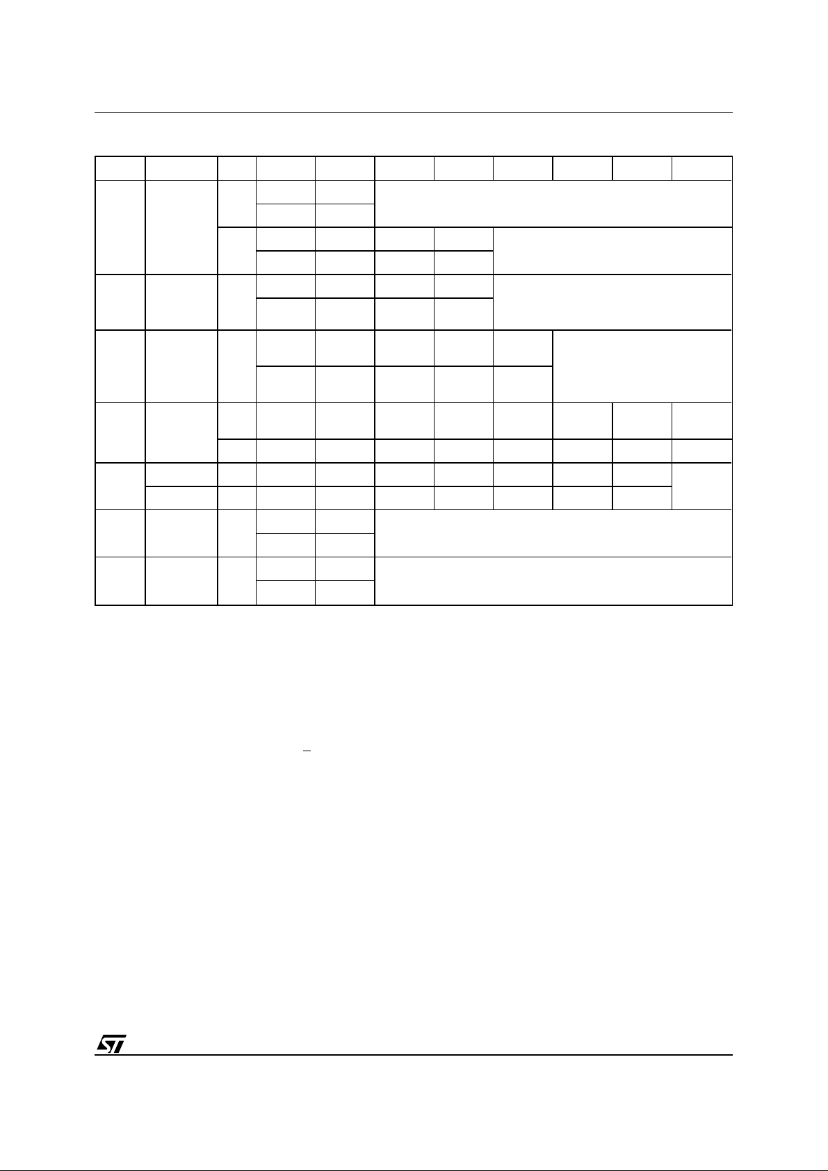
T ab le 8. Instructions
(1)
Mne. Instr. Cyc. 1st Cyc. 2nd Cyc. 3rd Cyc. 4th Cyc. 5th Cyc. 6th Cyc. 7th Cyc.
(3,7)
Addr.
RD
(2,4)
Read/Reset
Memory
Array
1+
3+
Data
Addr.
(3,7)
Data
(3,7)
Addr.
AS
(4)
Auto Select 3+
Data
(3,7)
Addr.
PG Program 4
Data
(3,7)
Addr.
BE Block Erase
6
Data
(3,7)
Chip Erase 6
CE
Addr.
Data
(3,7)
Addr.
Data
Addr.
Data
(3,7)
IL
ES
Notes:
Suspend
Erase
ER
Resume
1. Commands not interpreted in this table will default to read array mode.
2. A wait of t
before starting any new operation (See Table 14 and Figure 9).
3. X = Don’t Care.
4. The first cycles of the RD or AS instructions are followed by read operations. Any number of read cycles can occur after
the command cycles.
5. Signature Address bits A0, A1 at V
Device code.
6. Block Protection Address: A0 at V
7. For Coded cycles address inputs A15-A18 are don’t care.
8. Optional, additional Blocks addresses must be entered within the erase timeout delay after last write entry, timeout status
can be verified through DQ3 value (see Erase Timer Bit DQ3 description). When full command is entered, read Data Polling
or Toggle bit until Erase is completed or suspended.
9. Read Data Polling, T oggle bits or R
10.During Erase Suspend, Read and Data Program functions are allowed in blocks not being erased.
PLYH
1
1
is necessary after a Read/Reset command if the memory was in an Erase or Program mode
Erase
(10)
X
Read Memory Array until a new write cycle is initiated.
F0h
5555h 2AAAh 5555h
AAh 55h F0h
Read Memory Array until a new write cycle
is initiated.
5555h 2AAAh 5555h Read Electronic Signature or Block
Protection Status until a new write cycle is
AAh 55h 90h
5555h 2AAAh 5555h
AAh 55h A0h
5555h 2AAAh 5555h 5555h 2AAAh
initiated. See Note 5 and 6.
Program
Address
Program
Read Data Polling or Toggle Bit
until Program completes.
Data
Block
Address
AAh 55h 80h AAh 55h 30h 30h
5555h 2AAAh 5555h 5555h 2AAAh 5555h
AAh 55h 80h AAh 55h 10h
X
Read until Toggle stops, then read all the data needed from any
B0h
30h
will output Manufacturer code (20h). Address bits A0 at VIH and A1 at VIL will output
IL
, A1 at VIH and A13-A18 within the Block will output the Block Pr otec tio n st atus.
B until Erase completes.
Block(s) not being erased then Resume Erase.
X
Read Data Polling or Toggle Bits until Erase completes or Erase
is suspended another time
Additional
Block
Note 9
(8)
9/30
 Loading...