

FEATURES SUMMARY
■ SUPPLY VOLTAGE
–V
–V
■ ACCESS TIME: 90, 110ns
■ PROGRAMMING TIME
2.7V to 3.6V for Read
CC =
11.4V to 12.6V for Program and Erase
PP =
– 9µs per Word typical
– Multiple Word Programming Option (2s
typical Chip Program)
■ ERASE TIME
– 11s typical factory Chip Erase
■ UNIFORM BLOCKS
– 8 blocks of 2 Mbits
■ PROGRAM/ERA SE CONTROLLER
– Embedded Word Program algorithms
■ 10,000 PROGRAM/ERASE CYCLES per
BLOCK
■ ELECTRONIC SIGNATURE
– Manufacturer Code: 0020h
– Device Code : 88ABh
M29KW016E
16 Mbit (1Mb x16, Uniform Block)
3V Supply LightFlash™ Memory
PRELIMINARY DATA
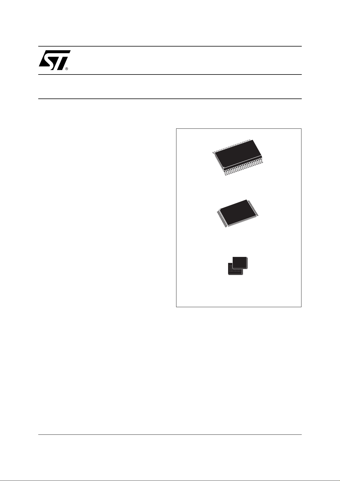
Figure 1. Packages
SO44 (M)
TSOP48 (N)
12 x 20mm
FBGA
TFBGA48 (ZA)
6 x 9mm
July 2002
This is preliminary information on a new product now in development or undergoing evaluation. Details are subject to change without notice.
1/31

M29KW016E
TABLE OF CONTENTS
FEATURES SUMMARY . . . . . . . . . . . . . . . . . . . . . . . . . . . . . . . . . . . . . . . . . . . . . . . . . . . . . . . . . . . . . 1
Figure 1. Packages . . . . . . . . . . . . . . . . . . . . . . . . . . . . . . . . . . . . . . . . . . . . . . . . . . . . . . . . . . . . . . 1
Table 1. Signal Names . . . . . . . . . . . . . . . . . . . . . . . . . . . . . . . . . . . . . . . . . . . . . . . . . . . . . . . . . . . 4
Figure 3. SO Connections. . . . . . . . . . . . . . . . . . . . . . . . . . . . . . . . . . . . . . . . . . . . . . . . . . . . . . . . . 5
Figure 4. TSOP Connections . . . . . . . . . . . . . . . . . . . . . . . . . . . . . . . . . . . . . . . . . . . . . . . . . . . . . . . 5
Figure 5. TFBGA Connections (Top view through package). . . . . . . . . . . . . . . . . . . . . . . . . . . . . . . 6
Table 2. Block Addresses . . . . . . . . . . . . . . . . . . . . . . . . . . . . . . . . . . . . . . . . . . . . . . . . . . . . . . . . . 6
SIGNAL DESCRIPTIONS . . . . . . . . . . . . . . . . . . . . . . . . . . . . . . . . . . . . . . . . . . . . . . . . . . . . . . . . . . . . 7
Address Inputs (A0-A19). . . . . . . . . . . . . . . . . . . . . . . . . . . . . . . . . . . . . . . . . . . . . . . . . . . . . . . . . . 7
Data Inputs/Outputs (DQ0-DQ7). . . . . . . . . . . . . . . . . . . . . . . . . . . . . . . . . . . . . . . . . . . . . . . . . . . . 7
Data Inputs/Outputs (DQ8-DQ15 ). . . . . . . . . . . . . . . . . . . . . . . . . . . . . . . . . . . . . . . . . . . . . . . . . . .7
Chip Enable (E). . . . . . . . . . . . . . . . . . . . . . . . . . . . . . . . . . . . . . . . . . . . . . . . . . . . . . . . . . . . . . . . . 7
Output Enable (G). . . . . . . . . . . . . . . . . . . . . . . . . . . . . . . . . . . . . . . . . . . . . . . . . . . . . . . . . . . . . . . 7
Write Enable (W). . . . . . . . . . . . . . . . . . . . . . . . . . . . . . . . . . . . . . . . . . . . . . . . . . . . . . . . . . . . . . . . 7
Reset (RP). . . . . . . . . . . . . . . . . . . . . . . . . . . . . . . . . . . . . . . . . . . . . . . . . . . . . . . . . . . . . . . . . . . . . 7
Ready/Busy Output (RB). . . . . . . . . . . . . . . . . . . . . . . . . . . . . . . . . . . . . . . . . . . . . . . . . . . . . . . . . . 7
V
Supply Voltage. . . . . . . . . . . . . . . . . . . . . . . . . . . . . . . . . . . . . . . . . . . . . . . . . . . . . . . . . . . . . . 7
CC
V
Program Supply Voltage . . . . . . . . . . . . . . . . . . . . . . . . . . . . . . . . . . . . . . . . . . . . . . . . . . . . . . 7
PP
Vss Ground.. . . . . . . . . . . . . . . . . . . . . . . . . . . . . . . . . . . . . . . . . . . . . . . . . . . . . . . . . . . . . . . . . . . . 7
BUS OPERATIONS. . . . . . . . . . . . . . . . . . . . . . . . . . . . . . . . . . . . . . . . . . . . . . . . . . . . . . . . . . . . . . . . . 8
Bus Read. . . . . . . . . . . . . . . . . . . . . . . . . . . . . . . . . . . . . . . . . . . . . . . . . . . . . . . . . . . . . . . . . . . . . . 8
Bus Write. . . . . . . . . . . . . . . . . . . . . . . . . . . . . . . . . . . . . . . . . . . . . . . . . . . . . . . . . . . . . . . . . . . . . . 8
Output Disable. . . . . . . . . . . . . . . . . . . . . . . . . . . . . . . . . . . . . . . . . . . . . . . . . . . . . . . . . . . . . . . . . . 8
Standby. . . . . . . . . . . . . . . . . . . . . . . . . . . . . . . . . . . . . . . . . . . . . . . . . . . . . . . . . . . . . . . . . . . . . . . 8
Automatic Standby. . . . . . . . . . . . . . . . . . . . . . . . . . . . . . . . . . . . . . . . . . . . . . . . . . . . . . . . . . . . . . . 8
Electronic Signature. . . . . . . . . . . . . . . . . . . . . . . . . . . . . . . . . . . . . . . . . . . . . . . . . . . . . . . . . . . . . . 8
Table 3. Bus Operations . . . . . . . . . . . . . . . . . . . . . . . . . . . . . . . . . . . . . . . . . . . . . . . . . . . . . . . . . . 8
COMMAND INTERFACE . . . . . . . . . . . . . . . . . . . . . . . . . . . . . . . . . . . . . . . . . . . . . . . . . . . . . . . . . . . . 9
Read/Reset Command.. . . . . . . . . . . . . . . . . . . . . . . . . . . . . . . . . . . . . . . . . . . . . . . . . . . . . . . . . . . 9
Auto Select Command. . . . . . . . . . . . . . . . . . . . . . . . . . . . . . . . . . . . . . . . . . . . . . . . . . . . . . . . . . . . 9
Word Program Command.. . . . . . . . . . . . . . . . . . . . . . . . . . . . . . . . . . . . . . . . . . . . . . . . . . . . . . . . . 9
Multiple Word Program Command . . . . . . . . . . . . . . . . . . . . . . . . . . . . . . . . . . . . . . . . . . . . . . . . . .9
Setup Phase . . . . . . . . . . . . . . . . . . . . . . . . . . . . . . . . . . . . . . . . . . . . . . . . . . . . . . . . . . . . . . . . 9
Program Phase. . . . . . . . . . . . . . . . . . . . . . . . . . . . . . . . . . . . . . . . . . . . . . . . . . . . . . . . . . . . . . 9
Verify Phase . . . . . . . . . . . . . . . . . . . . . . . . . . . . . . . . . . . . . . . . . . . . . . . . . . . . . . . . . . . . . . . 10
Exit Phase. . . . . . . . . . . . . . . . . . . . . . . . . . . . . . . . . . . . . . . . . . . . . . . . . . . . . . . . . . . . . . . . . 10
Block Erase Command.. . . . . . . . . . . . . . . . . . . . . . . . . . . . . . . . . . . . . . . . . . . . . . . . . . . . . . . . . . 10
Chip Erase Command. . . . . . . . . . . . . . . . . . . . . . . . . . . . . . . . . . . . . . . . . . . . . . . . . . . . . . . . . . . 10
Table 4. Standard Commands. . . . . . . . . . . . . . . . . . . . . . . . . . . . . . . . . . . . . . . . . . . . . . . . . . . . . 11
Table 5. Multiple Word Program Command . . . . . . . . . . . . . . . . . . . . . . . . . . . . . . . . . . . . . . . . . . 11
Table 6. Program, Erase Times and Program, Erase Endurance Cycles . . . . . . . . . . . . . . . . . . . . 11
Figure 6. Multiple Word Program Flowchart . . . . . . . . . . . . . . . . . . . . . . . . . . . . . . . . . . . . . . . . . . 12
2/31

M29KW016E
STATUS REGISTER. . . . . . . . . . . . . . . . . . . . . . . . . . . . . . . . . . . . . . . . . . . . . . . . . . . . . . . . . . . . . . . 13
Data Polling Bit (DQ7). . . . . . . . . . . . . . . . . . . . . . . . . . . . . . . . . . . . . . . . . . . . . . . . . . . . . . . . . . . 13
Toggle Bit (DQ6).. . . . . . . . . . . . . . . . . . . . . . . . . . . . . . . . . . . . . . . . . . . . . . . . . . . . . . . . . . . . . . . 13
Error Bit (DQ5). . . . . . . . . . . . . . . . . . . . . . . . . . . . . . . . . . . . . . . . . . . . . . . . . . . . . . . . . . . . . . . . . 13
VPP Status Bit (DQ4) . . . . . . . . . . . . . . . . . . . . . . . . . . . . . . . . . . . . . . . . . . . . . . . . . . . . . . . . . . . 13
Erase Timer Bit (DQ3). . . . . . . . . . . . . . . . . . . . . . . . . . . . . . . . . . . . . . . . . . . . . . . . . . . . . . . . . . . 13
Alternative Toggle Bit (DQ2).. . . . . . . . . . . . . . . . . . . . . . . . . . . . . . . . . . . . . . . . . . . . . . . . . . . . . . 13
Multiple Word Program Bit (DQ0) . . . . . . . . . . . . . . . . . . . . . . . . . . . . . . . . . . . . . . . . . . . . . . . . . . 13
Table 7. Multiple Word Program Timings . . . . . . . . . . . . . . . . . . . . . . . . . . . . . . . . . . . . . . . . . . . . 11
Table 8. Status Register Bits. . . . . . . . . . . . . . . . . . . . . . . . . . . . . . . . . . . . . . . . . . . . . . . . . . . . . . 14
Figure 7. Data Polling Flowchart . . . . . . . . . . . . . . . . . . . . . . . . . . . . . . . . . . . . . . . . . . . . . . . . . . . 1 4
Figure 8. Data Toggle Flowchart. . . . . . . . . . . . . . . . . . . . . . . . . . . . . . . . . . . . . . . . . . . . . . . . . . . 14
MAXIMUM RATING. . . . . . . . . . . . . . . . . . . . . . . . . . . . . . . . . . . . . . . . . . . . . . . . . . . . . . . . . . . . . . . . 15
Table 9. Absolute Maximum Ratings. . . . . . . . . . . . . . . . . . . . . . . . . . . . . . . . . . . . . . . . . . . . . . . .15
DC and AC PARAMETERS . . . . . . . . . . . . . . . . . . . . . . . . . . . . . . . . . . . . . . . . . . . . . . . . . . . . . . . . . 16
Table 10. Operating and AC Measurement Conditions. . . . . . . . . . . . . . . . . . . . . . . . . . . . . . . . . . 16
Figure 9. AC Measurement I/O Waveform . . . . . . . . . . . . . . . . . . . . . . . . . . . . . . . . . . . . . . . . . . .16
Figure 10. AC Measurement Load Circuit. . . . . . . . . . . . . . . . . . . . . . . . . . . . . . . . . . . . . . . . . . . . 16
Table 11. Device Capacitance . . . . . . . . . . . . . . . . . . . . . . . . . . . . . . . . . . . . . . . . . . . . . . . . . . . . . 16
Table 12. DC Characteristics. . . . . . . . . . . . . . . . . . . . . . . . . . . . . . . . . . . . . . . . . . . . . . . . . . . . . . 17
Figure 11. Read AC Waveforms . . . . . . . . . . . . . . . . . . . . . . . . . . . . . . . . . . . . . . . . . . . . . . . . . . . 18
Table 13. Read AC Characteristics . . . . . . . . . . . . . . . . . . . . . . . . . . . . . . . . . . . . . . . . . . . . . . . . . 18
Figure 12. Write AC Waveforms, Write Enable Controlled . . . . . . . . . . . . . . . . . . . . . . . . . . . . . . . 19
Table 14. Write AC Characteristics, Write Enable Controlled . . . . . . . . . . . . . . . . . . . . . . . . . . . . . 20
Figure 13. Write AC Waveforms, Chip Enable Controlled . . . . . . . . . . . . . . . . . . . . . . . . . . . . . . . . 21
Table 15. Write AC Characteristics, Chip Enable Controlled . . . . . . . . . . . . . . . . . . . . . . . . . . . . . 22
Figure 14. Reset AC Waveforms . . . . . . . . . . . . . . . . . . . . . . . . . . . . . . . . . . . . . . . . . . . . . . . . . . . 23
Table 16. Reset AC Characteristics . . . . . . . . . . . . . . . . . . . . . . . . . . . . . . . . . . . . . . . . . . . . . . . . 23
PACKAGE MECHANICAL . . . . . . . . . . . . . . . . . . . . . . . . . . . . . . . . . . . . . . . . . . . . . . . . . . . . . . . . . . 24
Figure 15. SO44 - 44 lead Plastic Small Outline, 525 mils body width, Package Outline . . . . . . . . 24
Table 17. SO44 - 44 lead Plastic Small Outline, 525 mils body width, Package Mechanical Data . 24
Figure 16. TSOP48 - 48 lead Plastic Thin Small Outline, 12 x 20mm, Package Outline . . . . . . . . 25
Table 18. TSOP48 - 48 lead Plastic Thin Small Outline, 12 x 20mm, Package Mechanical Data . 25
Figure 17. TFBGA48 6x9mm - 8x6 ball array, 0.80 mm pitch, Bottom View Package Out line . . . . 26
Table 19. TFBGA48 6x9mm - 8x6 ball array, 0.80 mm pitch, Package Mechanical Data. . . . . . . . 26
Figure 18. TFBGA48 Daisy Chain - Package Connections (Top view through package) . . . . . . . . 27
Figure 19. TFBGA48 Daisy Chain - PCB Connections (Top view through package) . . . . . . . . . . . 28
PART NUMBERING . . . . . . . . . . . . . . . . . . . . . . . . . . . . . . . . . . . . . . . . . . . . . . . . . . . . . . . . . . . . . . . 29
Table 20. Ordering Information Scheme . . . . . . . . . . . . . . . . . . . . . . . . . . . . . . . . . . . . . . . . . . . . .29
Table 21. Daisy Chain Ordering Scheme . . . . . . . . . . . . . . . . . . . . . . . . . . . . . . . . . . . . . . . . . . . . 29
REVISION HISTORY. . . . . . . . . . . . . . . . . . . . . . . . . . . . . . . . . . . . . . . . . . . . . . . . . . . . . . . . . . . . . . . 30
Table 22. Document Revision History . . . . . . . . . . . . . . . . . . . . . . . . . . . . . . . . . . . . . . . . . . . . . . .30
3/31
M29KW016E
SUMMARY DESCRIPTION
The M29KW016E L ightFlash™ is a 16 Mbit (1Mb
x16) non-volatile memory that can be read, erased
and reprogrammed. Read op erations can b e performed using a single low voltage (2.7 to 3.6V)
supply. Program an d Er ase operations require an
additional V
power-up the memory defaults to its Read mode
where it can be read in the same way as a ROM or
EPROM.
The memory is divide d into 8 uniform bl ocks that
can be erased i ndependently so it is poss ible to
preserve valid data whi le old data is erased (see
Figures 2, Block Address es). Program a nd Erase
commands are written to the Command Interface
of the memory. An on-chip Program/Erase Controller (P/E.C.) simplifies the process of programming or erasing the memory by taking care of all of
the special operations that are required to update
the memory contents.
The M29KW016E LightFlash™ features a new
command, Multiple Word Program, used to program large streams of dat a. I t g reatly reduc es t he
total programming time when a large number of
Words are written to the memory at any one time.
Using this command the entire memory can be
programmed in 2s, compared to 9s using the standard Word Program.
The end of a program or erase operation can be
detected and any error conditions identified. The
command set required to control the memory is
consistent with JEDEC standards.
Chip Enable, Output Enable and Write Enable signals control the bus operation of the memory.
They allow simple conne ction to most m icroprocessors, often without additional logic.
The memory is offered in SO44, TSOP48 (12 x
20mm) and TFBGA48 (6 x 9mm, 0.8mm pitch)
packages. The memory is supplied with all the bits
erased (set to ’1’).
(11.4 to 12.6) power supply. On
PP
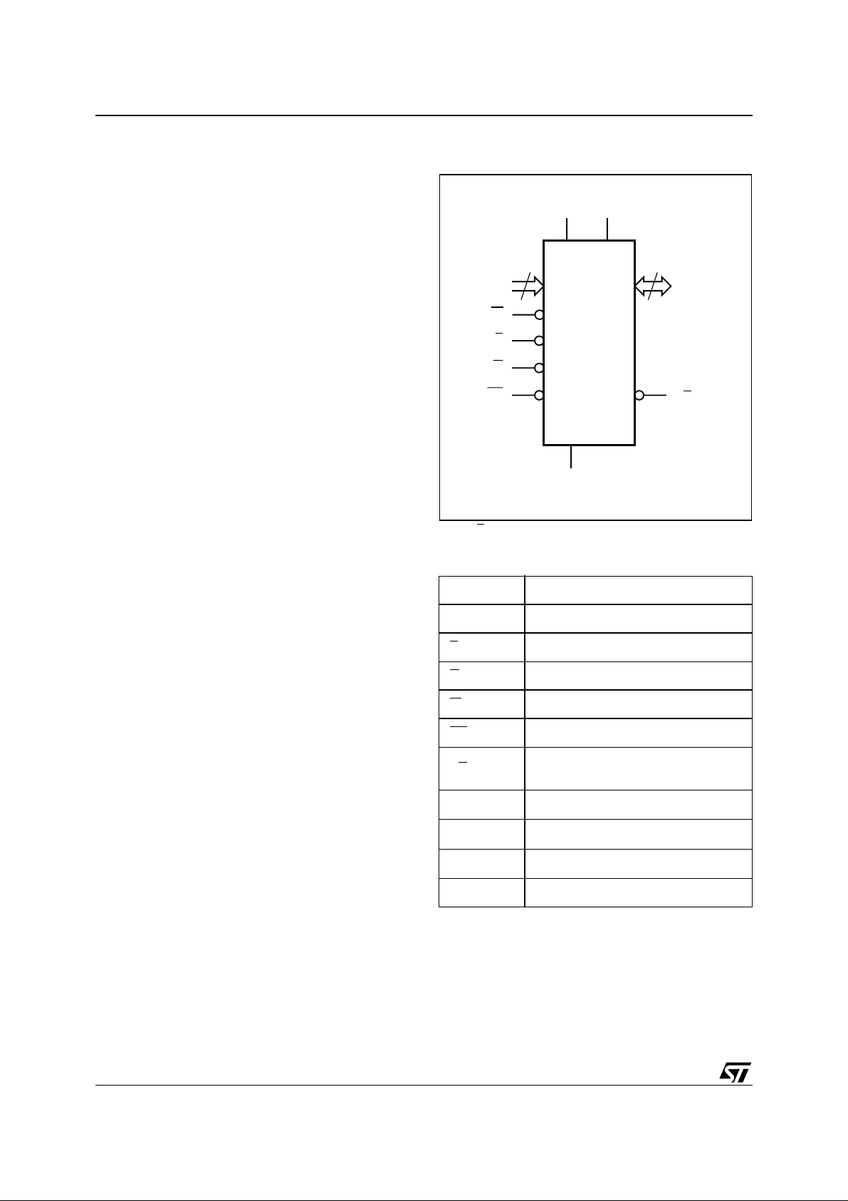
Figure 2. Logic Diagram
V
V
20
A0-A19 DQ0-DQ15
W
E
G
RP
Note: RB not availab l e on SO44 pa ckage.
M29KW016E
V
CC
SS
PP
16
RB
Table 1. Signal Names
A0-A19 Address Inputs
DQ0-DQ15 Data Inputs/Outputs
E
G
W
RP
RB
Chip Enable
Output Enable
Write Enable
Reset
Ready/Busy Output
(not available on SO44 package)
AI04371
4/31
V
CC
V
PP
V
SS
NC Not Connected Internally
Supply Voltage read
Supply Voltage program erase
Ground
Figure 3. SO Connections Figure 4. TSOP Connections
M29KW016E
A7
A6
A5
A4
A3
A2
A1
A0
1
2
3
4
5
6
7
8
9
10
11
M29KW016E
12
E
13
14
G
15
16
RP
A18
A17 A8
V
SS
DQ0
DQ8
17DQ1
DQ9
18
19
DQ10
DQ3
20
21
DQ11
44
43
42
41
40
39
38
37
36
35
34
33
32
31
30
29
28
27
26
25
24
2322
W
A19
A9
A10
A11
A12
A13
A14
A15
A16
V
PP
V
SS
DQ15
DQ7
DQ14
DQ6
DQ13
DQ5DQ2
DQ12
DQ4
V
CC
A15
A14
A13
A12
A11
1
48
A16
NC
V
SS
DQ15
DQ7
A10 DQ14
A9
A8
A19
NC
W
RP
NC
V
PP
RB
A18
A17
A7
A6
A5
A4
A3
A2
A1
12
M29KW016E
13
37
36
24 25
DQ6
DQ13
DQ5
DQ12
DQ4
V
CC
DQ11
DQ3
DQ10
DQ2
DQ9
DQ1
DQ8
DQ0
G
V
SS
E
A0
AI04377
AI04376b
5/31
M29KW016E
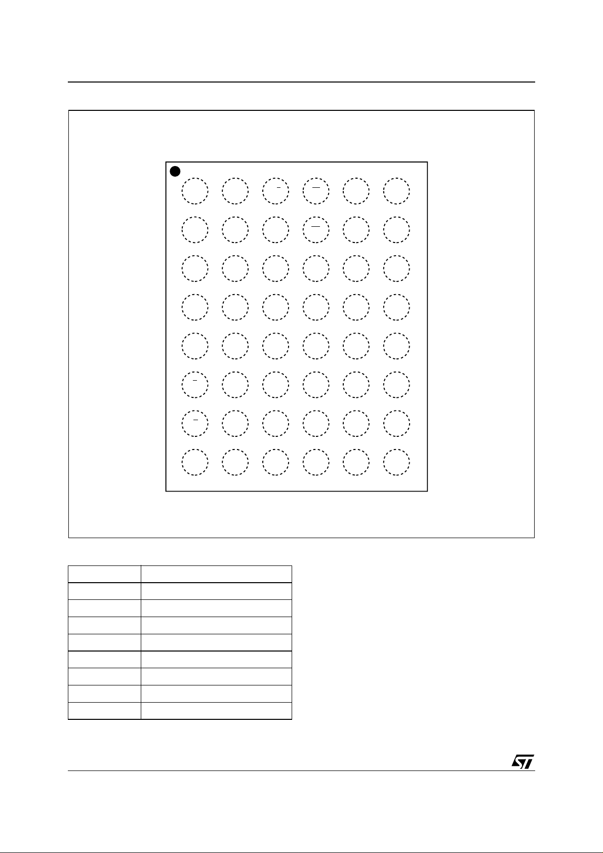
Figure 5. TFBGA Connections (Top view through package)
654321
A
B
C
D
E
F
G
H
A3
A4
A2
A1
A0
E
G
V
SS
A7
A17
A6
A5
DQ0
DQ8
DQ9
DQ1
RB
V
PP
A18
NC
DQ2
DQ10
DQ11
DQ3
W
RP
NC
A19
DQ5
DQ12
V
CC
DQ4
A9
A8
A10
A11
DQ7
DQ14
DQ13
DQ6
A13
A12
A14
A15
A16
NC
DQ15
V
SS
Table 2. Block Addresses
Block Number Address Range
8 E0000h-FFFFFh
7 C0000h-DFFFFh
6 A0000h-BFFFFh
5 80000h-9FFFFh
4 60000h-7FFFFh
3 40000h-5FFFFh
2 20000h-3FFFFh
1 00000h-1FFFFh
6/31
AI04373

SIGNAL DESCRIPTIONS
See Figure 2, Logic Diagram, and Table 1, Sign al
Names, for a brief overview of the signals connected to this device.
Address Inputs (A0-A19). The Address Inputs
select the cells i n the memory array to a ccess during Bus Read operations. During Bus Write operations they control the commands sent to the
Command Interface of the Program/Erase Controller.
Data Inputs/Outputs (DQ0-DQ7). The Data Inputs/Outputs outputs the data stored at the selected address during a Bus Rea d operation. Du ring
Bus Write operations they represent the commands sent to the Command Interface of the Program/Erase Controller.
Data Inputs/Outputs (DQ8-DQ15). The Data Inputs/Outputs output the data stored at the selected
address during a Bus Read operation. During Bus
Write operations the Command Register does not
use these bits. When reading t he Status Register
these bits should be ignored.
Chip Enable (E
). The Chip Enable, E, activates
the memory, allowing Bus Read and Bus Write operations to be performed. When Chip Enable is
High, V
Output Enable (G
, all other pins are ignored.
IH
). The Output Enable, G, con-
trols the Bus Read operation of the memory.
Write Enable (W
). The Write Enable, W, controls
the Bus Write operation of the memory’s Command Interf a c e .
Reset (RP
). The Reset pin can be used to apply
a Hardware Reset to the memory.
A Hardware Reset is achieved by holding Reset
Low, V
V
IH
Bus Write operations after t
, fo r at least t
IL
. After Reset goes High,
PLPX
, the memory will be ready for B us Read and
PHEL
or t
RHEL
, which ever occurs last. See the Ready/Busy Output section, Table 16 and Figure 14, Reset AC
Characteristics for more details.
Ready/Busy Output (RB
). The Ready/Busy pin
is an open-drain output that can be used to identify
when the memory array can be read. Ready/Busy
is high-impedance during Read mode and Auto
Select mode. After a Hardware Reset, Bus Read
and Bus Write operations cannot begin until
M29KW016E
Ready/Busy becomes high-impedance. See Table
16 and Figure 14, Reset AC Characteristics.
During Program or Erase operations Ready/Busy
is Low, V
Read/Reset commands or Hardw are Resets until
the memory is ready to enter Read mode.
The use of an open-drain output allows the Ready/
Busy pins from several memories to be connected
to a single pull-up resistor. A Low will then indicate
that one, or more, of the memories is busy.
Supply Voltage. The VCC Supply Voltage
V
CC
supplies the power for Read operations.
The Command Interface is disabled when the V
Supply Voltage is less than the L ockout Voltage,
V
. This prevents Bus Write operations from ac-
LKO
cidentally damaging the data during power up,
power down and power surges. If the Program/
Erase Controller is programming or erasing during
this time then the operation aborts and the memory contents being altered will be invalid.
A 0.1µF capacitor should be connected between
the V
pin to decouple the current surges from the power
supply. The PCB track widths must be sufficient to
carry the currents required during program and
erase operations, I
Program Supply Voltage. VPP is both a
V
PP
power supply and Write Protect pin. The two functions are selected by t he voltage range a pplied t o
the pin. The Supply Voltage V
before the Program Supply Voltage V
If V
PP
power supply pin for program and erase operations. V
algorithm is completed.
If V
PP
V
is seen as a Write Protect pin. In this case a
PP
voltage lower than V
tion against program or erase, while V
range of V
12, DC Characteristics for the relevant values).
Note that V
nected as the device may become unreliable.
Vss Ground. The V
for all voltage measurements.
. Ready/Busy will remain Low during
OL
Supply Voltage pin and the VSS Ground
CC
.
CC3
must be applied
CC
PP
.
is in the range 11.4V to 12.6V it acts as a
must be stable until the Program/Erase
PP
is kept in a low voltage range (0V to 3.6V)
gives an absolute p rotec-
HH
enables these functions (se e Table
HH
must not be left floating o r uncon-
PP
Ground is the reference
SS
in the
PP
CC
7/31
M29KW016E
BUS OPERATIONS
There are six standard bus operations that control
the device. These are Bus Read, Bus Wri te, Output Disable, Standby, Automatic Standby and
Electronic Signature. See Tables 3, Bus Operations, for a summary. Typically glitches of less
than 5ns on Chip Enable or Write Enable are ignored by the memory and do not affect bus operations.
Bus Read. Bus Read operations read from the
memory cells, or specific registers in the Command Interface. A valid Bus Read operation involves setting the desired address on the Address
Inputs, applying a Low sig nal, V
and Output Enable and keeping Write Enable
High, V
. The Data Inputs/Outputs will output the
IH
value, see Figure 11, Read Mode AC Waveforms,
and Table 13, Read AC Characteristics, for details
of when the output becomes valid.
Bus Write. Bus Write operations write to the
Command Interface. A valid Bus Write operation
begins by setting the desire d address on t he Address Inputs. The Address Inputs are latched by
the Command Interface on the falling edge of Chip
Enable or Write Enable, whichever occurs last.
The Data Inputs/Outputs a re latched by the Command Interface on the rising edge of Chip Enable
or Write Enable, whichever occurs first. Output Enable must remain High, V
IH
Write operation. See Figures 12 and 13, Write AC
Waveforms, and Tables 14 and 15, Write AC
, to Chip Enable
IL
, during the whole Bus
Characteristics, for details of the timing requirements.
Output Disa bl e . The Data Inputs/Outputs are in
the high impedance s tate when Output Enable is
High, V
Standby. When Chip Enable is High, V
.
IH
, the
IH
memory enters Standby mode and the Data Inputs/Outputs pins are placed in the high-impedance state. To reduce the S upply Current to the
Standby Supply Current, I
be held within V
± 0.2V. For the Standby current
CC
, Chip Enable should
CC2
level see Table 12, DC Characteristics.
During program or erase operations the memory
will continue to use the Program/Erase Supply
Current, I
, for Program or Erase operations un-
CC3
til the operation completes.
Automatic Standby. If CMOS levels (V
± 0.2V)
CC
are used to drive the bus and the bus is inactive for
150ns or more the memory enters Automatic
Standby where the internal Supply Current is reduced to the Standby Supply Current, I
CC2
. The
Data Inputs/Outputs will still output data if a Bus
Read operation is in progress.
Electronic Signature. The memory has two
codes, the manufacturer code and the device
code, that can be read to identify the memory.
These codes can be read by applying t he signals
listed in Tables 3, Bus Operations.
Table 3. Bus Operations
V
V
XX
PP
HH
X
XX
XX
Operation E G W
V
IL
V
IH
V
IH
X X X X Hi-Z
V
IL
V
IL
or V
HH
V
IL
V
IL
V
IH
V
IL
V
IL
Bus Read
Bus Write
Output Disable X
Standby
Read Manufacturer
Code
Read Device Code
Note: 1. X = VIL or VIH.
2. XX = V
3. Not necessary for A uto Select or Read/Res et command s.
4. When re adi ng the Status Register during Program or Eras e operations, V
, V
IL
IH
V
IH
V
IL
V
IH
V
IH
V
IH
Address Inputs
A0-A19
(4)
Cell Address Data Output
(3)
Command Address Data Input
X Hi-Z
A0 = V
Others V
A0 = V
Others V
, A1 = VIL,
IL
or V
IL
IH
, A1 = VIL,
IH
or V
IL
IH
must be kept at VHH.
PP
Data Inputs/Outputs
DQ15-DQ0
0020h
88ABh
8/31

COMMAND INTERFACE
All Bus Write operations t o the me mory are in terpreted by the Command Interface. Commands
consist of one or more sequential Bus Write operations. Failure to observe a valid sequence of Bus
Write operations will result in the memory returning to Read mode. The long command sequences
are imposed to maximize data security.
Refer to Tables 4 and 5, for a summary of the commands.
Read/Reset Command.
The Read/Reset command returns the memory to
its Read mode where it behaves like a ROM or
EPROM, unless otherwise stated. It also resets
the errors in the Status Register. Either one or
three Bus Write operations can be u sed to issue
the Read/Reset command.
The Read/Reset Command can be issued, between Bus Write cycles before the start of a program or erase operation, to return the device to
read mode. Once the program or erase operation
has started the Read/Reset command is no longer
accepted. The Read/Res et co mmand is executed
regardless of the value of V
(VIL, VIH or VHH).
PP
Auto Select Command.
The Auto Select command is used to read the
Manufacturer Code and the Device Code. Three
consecutive Bus Write operations are re quired to
issue the Auto Selec t command. Onc e the Auto
Select command is issued the memory remains in
Auto Select mode until a Read/Reset command is
issued, all other commands are ignored. The Auto
Select command is executed regardless of the value of V
(VIL, VIH or VHH).
PP
From the Auto Select mode the Manufacturer
Code can be read using a Bus Read operation
with A0 = V
may be set to either V
and A1 = VIL. The other address bits
IL
or VIH.
IL
The Device Code can be read using a B us Read
operation with A0 = V
address bits may be set to either V
and A1 = VIL. The other
IH
or VIH.
IL
Word Progr a m Com m a n d.
The Word Program command can be used to program a Word to the memory array. V
set to V
ther V
during Word Program. If VPP is set to ei-
HH
or VIH the command will be ignored, the
IL
must be
PP
data will remain unchanged and the device will revert to Read/Reset mode. The command requires
four Bus Write operations, the final write operation
latches the address and data in the internal state
machine and starts the Program/Erase Controller.
During the program operat ion the memo ry will ignore all commands. I t is n ot poss ible t o iss ue any
command to abort or pause the operation. Typical
program times are given in Table 6. Bus Read operations during the program o peration will output
M29KW016E
the Status Register on the Data Inputs/Outputs.
See the section on the S tatus Register for more
details.
After the program operation has completed the
memory will return to the Read mode, unle ss an
error has occurred. When an error occurs the
memory will continue to output the Status Register. A Read/Reset command must be issued to reset the error condition and return to Read mode.
Note that the Program command cannot change a
bit set at ’0’ bac k to ’1’. One of the E rase Commands must be used to set all the bits in a block or
in the whole memory from ’0’ to ’1’.
Multiple Word Program Command
The Multiple Word Program command can be
used to program large streams of data. It greatly
reduces the total programming time when a l arge
number of Words are written to the memory at any
one time. V
Word Progr am. If V
command will be ignored, the data will remain unchanged and the device will revert to Read/Reset
mode.
It has four phases : the Set up P ha se to initiate t he
command, the Program Phase to program the
data to the memory, the Verify Phase to check that
the data has been correctly programmed and reprogram if necessary and the Exit Phase.
Setup Phase. The M ultiple Word Program command requires three Bus Write operations to initiate the command (refer to Table 5, Multiple Word
Program Command and Figure 6, Multiple Word
Program Flowchart). The Status Register Toggle
bit (DQ6) should be checked to verify that the operation has started and the Multiple Word Program
bit (DQ0) checked to verify that the P/E.C. is ready
for the first Word.
Program Phase. The Program Phase requires
n+1 cycles, where n is the number of Words, to execute the programming phase (refer to Table 5,
Multiple Word Program Command and Figure 6,
Multiple Word Program Flowchart).
Three successive steps are required to issue and
execute the Program Phase of the command.
1. The fourth Bus Write operation of the command
latches the Start Address and the first Word to
be programmed. The Status Register Multiple
Word Program bit (DQ0) should be read to
check that the P/E.C. is ready for the next Word.
2. Each subsequent Word to be programmed is
latched with a new Bus Write operation. The
address can remain the Start Address, be
incremented or be any address in the same
block, as the device automatically increments
the address with each sucssesive Bus Write
must be set to VHH during Multiple
PP
is set to e ither V
PP
or VIH the
IL
9/31

M29KW016E
cycle. If the command is used to program in
more than one block then the address must
remain in the starting block as any address that
is not in the same block as the Start Address
terminates the Program operation. The Status
Register Multiple Word Program bit (DQ0) must
be read between each Bus Write cycle to check
that the P/E.C. is ready for the next Word.
3. Finally, after all Words have been programmed,
write one Bus Write operat ion to any address
outside the block containing the Sta rt Address,
to terminate the programming phase.
The memory is now set to enter the Verify Phase.
Verify Phase. Th e Verify Phase is s imilar to the
Program Phase in that all Words must be resent to
the memory for them to be che cked against the
programmed data. If the ch eck fails the P /E.C wi ll
try to reprogram the correct data. The P/E.C will
remain busy until the correct data has been successfully programmed. The Verify Phase is mandatory. If the Verify Phase is not executed the
programmed data cannot be guaranteed.
Three successive steps are required to execute
the Verify Phase of the command.
1. Us e one Bus Write operation to latch the Start
Address and the first Word, to be verified. The
Status Register Multiple Word Program bit
(DQ0) should be read to check that the P/E.C. is
ready for the next Word.
2. Each subsequent Word to be verified is latched
with a new Bus Write operation. If any address
that is not in the same block as the Start
Address is given, the Verify operation
terminates. The Status Register Multiple Word
Program (DQ0) must be read to check that the
P/E.C. is ready for the next Word.
3. Finally, after all Words have been verified, write
one Bus Write operation to any address outside
the block containing the Start Address, to
terminate the Verify Phase.
Exit Phase . Read the Status Register to verify
that DQ6 has stopped toggling. If the Verify Phase
is successfully completed the memory returns to
the Read mode. If the P/E.C. fails to reprogram a
given location, the Verify Phase will terminate and
Error bit DQ5 will be set in the Status Register. If
the error is due to a V
failure DQ4 w ill als o be
PP
set. If the operation fails a R ead/Res et comm and
must be issued to return the device to Read mode.
It is not possible to issue any command to abort or
pause the operation. Typical program times are
given in Table 6. Bus Read operations du ring the
program operatio n will outpu t the Sta tus Regi ster
on the Data Inputs/Outputs. See the section on the
Status Register for more details.
Note that the Multiple Word Program command
cannot change a bit set at ’0’ back to ’1’. One of the
Erase Commands must be used to set all the bits
in a block or in the whole memory from ’0’ to ’1’.
Block Erase Command.
The Block Erase com mand can be used to erase
a block. It sets all of the bits in the block to ’1’. All
previous data in the block is lost.
must be set to VHH during Block Erase. If V
V
PP
is set to either V
or VIH the command will be ig-
IL
PP
nored, the data will remain unchanged and the device will revert to Read/Reset mode.
Six Bus Write operations are required to select the
block . The Block Erase operation starts the Program/Erase Controller after the last Bus Write operation. The Status Register can be read after the
sixth Bus Write operation. See the Status Register
for details on how to identify if the P rogram /Erase
Controller has started the Block Erase operation.
During the Block Erase operation the me mory wi ll
ignore all commands. Typical block erase times
are given in Table 6. All Bus Read operations during the Block Erase operation will output the Status Register on the Data Inputs/Outputs. See the
section on the Status Register for more details.
After the Block Erase operation has completed the
memory will return to the Read Mode, unle ss an
error has occurred. When an error occurs the
memory will continue to output the Status Register. A Read/Reset command must be issued to reset the error condition and return to Read mode.
Chip Erase Command.
The Chip Erase command can be used to erase
the entire memory. It sets all of the bits in the memory to ’1’. All previous data in the memory is lost.
must be set to VHH during Chip Erase. If V
V
PP
is set to either V
or VIH the command will be ig-
IL
PP
nored, the data will remain unchanged and the device will revert to Read/Reset mode. Six Bus Write
operations are required to issue the Chip Erase
Command and start the Program/Erase Controller.
During the erase operation the memory will ignore
all commands. It is not possible to issue any command to abort the operation. Typical chip erase
times are given in Table 6. All Bus Read operations during the Chip E rase operation will output
the Status Register on the Data Inputs/Outputs.
See the section on the S tatus Register for more
details.
After the Chip Erase operation has completed t he
memory will return to the Read Mode, unle ss an
error has occurred. When an error occurs the
memory will continue to output the Status Register. A Read/Reset command must be issued to reset the error condition and return to Read Mode.
10/31
 Loading...