

SGS Thomson Microelectronics M28C16 Datasheet
16K (2K x 8) PARALLELEEPROM
with SOFTWARE DATA PROTECTION
FASTACCESSTIME: 90ns
SINGLE 5V ± 10% SUPPLYVOLTAGE
LOW POWERCONSUMPTION
FASTWRITECYCLE:
– 64 Bytes Page WriteOperation
– Byte or Page Write Cycle: 3ms Max
ENHANCED END OF WRITEDETECTION:
– Data Polling
– ToggleBit
PAGELOAD TIMER STATUS BIT
HIGH RELIABILITYSINGLEPOLYSILICON,
CMOS TECHNOLOGY:
– Endurance >100,000Erase/WriteCycles
– Data Retention >40 Years
JEDEC APPROVEDBYTEWIDEPIN OUT
SOFTWAREDATA PROTECTION
M28C16 is replacedby the products
describedon the documentM28C16A
DESCRIPTION
The M28C16 is a 2K x 8 low power Parallel
EEPROMfabricatedwithSGS-THOMSONproprietary single polysilicon CMOS technology.The device offers fast access time with low power
dissipation and requires a 5V power supply. The
circuithas been designed to offer a flexible microcontroller interface featuring both hardware and
softwarehandshakingwithDataPollingandToggle
Bit. The M28C16 supports 64 byte page write operation. A Software Data Protection (SDP) is also
possibleusing the standard JEDECalgorithm.
Table 1. Signal Names
A0 - A10 Address Input
DQ0 - DQ7 Data Input / Output
W Write Enable
E Chip Enable
G Output Enable
RB Ready / Busy
V
CC
V
SS
Supply Voltage
Ground
M28C16
NOT FOR NEW DESIGN
24
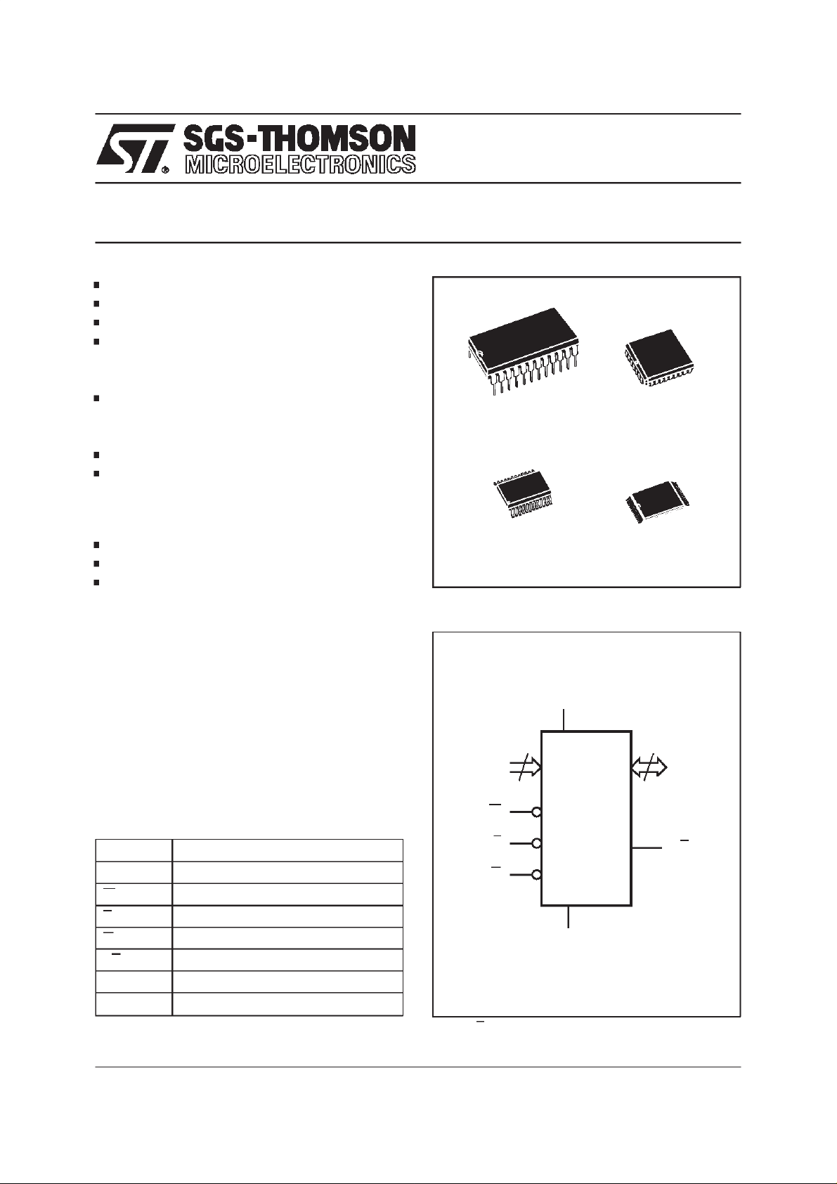
1
PDIP24 (P) PLCC32 (K)
24
1
SO24 (MS)
300 mils
Figure 1. Logic Diagram
V
CC
11
A0-A10
W
E
G
Note: * RB function is offered only with TSOP28 package.
M28C16
V
SS
TSOP28 (N)
8 x13.4mm
8
DQ0-DQ7
RB *
AI01518B
November 1997 1/18
This isinformation on a product still in production but not recommendedfor new design.
M28C16
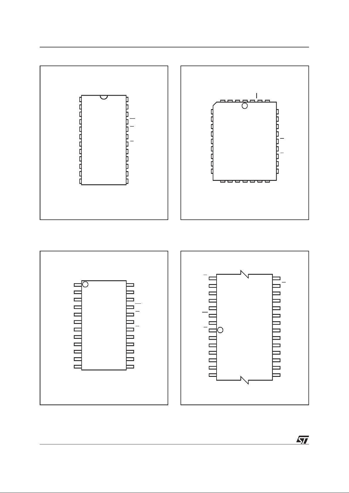
Figure2A. DIPPin Connections
A7
1
A6
2
A5
3
A4
4
A3
5
A2
6
A1
7
A0
8
DQ0
9
10
DQ2
11
12 13
SS
M28C16
24
23
22
21
20
19
18
17
16
15
14
AI01485
V
CC
A8
A9
W
G
A10
E
DQ7
DQ6
DQ5DQ1
DQ4
DQ3V
Figure2B. LCC Pin Connections
CC
NC
DU
32
W
V
A8
A9
NC
NC
G
25
A10
E
DQ7
DQ6
DQ4
DQ5
AI01486C
NC
A7
NC
1
A6
A5
A4
A3
A2
9
M28C16
A1
A0
NC
DQ0
17
SS
V
DQ1
DQ2DUDQ3
Warning: NC = Not Connected, DU = Don’t Use
Figure2C. SO Pin Connections
A7
A6
A5
A3
A2
A1
A0
DQ0
DQ1
DQ2
V
SS
1
2
3
4
5
6
7
8
9
10
11
12
M28C16
24
23
22
21
20
19
18
17
16
15
16
15
AI01519
V
CC
A8
A9
WA4
G
A10
E
DQ7
DQ6
DQ5
DQ4
DQ3
Figure2D. TSOPPin Connections
G
22
NC
A9
A8
NC
W
V
CC
RB
28
1
M28C16
NC
A7
A6
A5
A4
A3
Warning: NC = Not Connected.
78
21
15
14
AI01175C
A10
E
DQ7
DQ6
DQ5
DQ4
DQ3
V
SS
DQ2
DQ1
DQ0
A0
A1
A2
2/18
M28C16
Table 2. Absolute Maximum Ratings
Symbol Parameter Value Unit
T
A
T
STG
V
CC
V
IO
V
V
ESD
Notes: 1. Except for therating ”Operating Temperature Range”, stresses above those listed in the Table”Absolute Maximum Ratings” may
2. 100pF through 1500Ω; MIL-STD-883C, 3015.7
Table 3. Operating Modes
Standby 1 X X Hi-Z
Output Disable X 1 X Hi-Z
Write Disable X X 1 Hi-Z
Ambient Operating Temperature – 40 to 125 °C
Storage Temperature Range – 65 to 150 °C
Supply Voltage –0.3 to 6.5 V
Input/Output Voltage – 0.3 to VCC+0.6 V
Input Voltage –0.3 to 6.5 V
I
Electrostatic Discharge Voltage (Human Body model)
cause permanent damage to the device. These are stress ratings only and operation of the device at these or any other conditions
above those indicated in the Operating sections of this specification is not implied. Exposure toAbsolute Maximum Rating
conditions for extended periods may affect devicereliability. Refer also to the SGS-THOMSON SURE Program and other
relevant quality documents.
(1)
Mode E G W DQ0 - DQ7
(1)
(2)
4000 V
Read 0 0 1 Data Out
Write 0 1 0 Data In
Chip Erase 0 V 0 Hi-Z
Note: 1. 0 = VIL;1=VIH;X=VILor V
PIN DESCRIPTION
Addresses (A0-A10). The address inputs select
an 8-bit memory location during a read or write
operation.
Chip Enable (E). The chip enable input must be
low to enable all read/writeoperations.When Chip
Enableis high,powerconsumption is reduced.
Output Enable(G). The Output Enableinput controls the data output buffers and is used to initiate
read operations.
DataIn/Out(DQ0- DQ7).Data iswrittento orread
from the M28C16through the I/O pins.
WriteEnable(W). TheWrite Enableinput controls
the writing of data to the M28C16.
Ready/Busy (RB). Ready/Busy is an open drain
output that can be used to detect the end of the
internal writecycle.
It is offeredonly withthe TSOP28package. The
V= 12±5%.
IH;
OPERATION
In orderto prevent datacorruption andinadvertent
write operationsan internal V
its Write operation if V
CC
comparatorinhib-
CC
is below VWI(see Table
7). Accessto thememory in writemode is allowed
after a power-up as specified in Table 7.
Read
The M28C16is accessed likea staticRAM. When
E and G are low with W high, the dataaddressed
is presentedon the I/O pins. The I/O pins are high
impedancewhen either G orE is high.
Write
Write operations are initiatedwhen both W and E
are low and G is high.The M28C16 supports both
E and W controlled write cycles. The Address is
latched by the falling edge of E or W which ever
occurs last and the Data on the rising edgeof E or
W which ever occurs first. Once initiated the write
operationis internally timed until completion.
readershouldrefertotheM28C17datasheetfor
more information about the Ready/Busy function.
3/18
M28C16
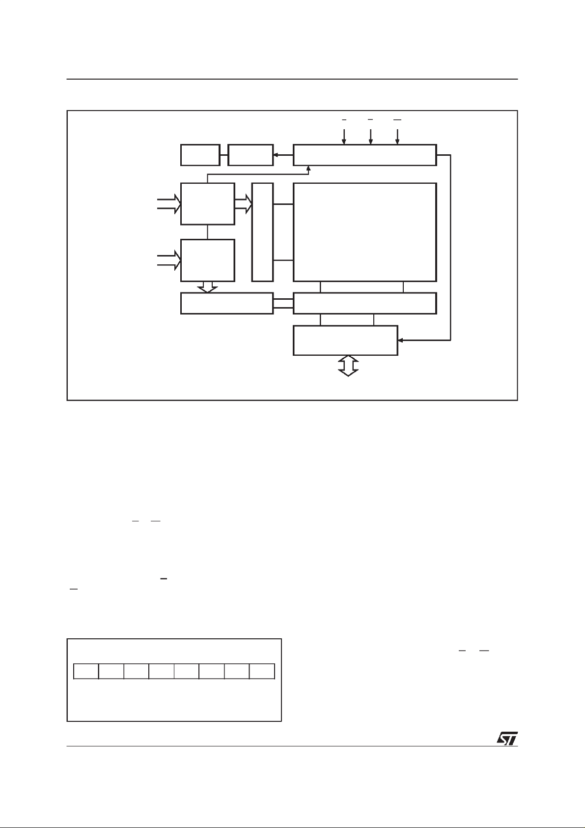
Figure3. Block Diagram
EGW
VPPGEN RESET
A6-A10
(Page Address)
A0-A5
ADDRESS
LATCH
ADDRESS
LATCH
Y DECODE
X DECODE
Page Write
Page write allows up to 64 bytes to be consecutively latched into the memory prior to initiating a
programmingcycle. All bytes must be located in a
single page address, that is A6-A10must be the
samefor all bytes. Thepage write canbe initiated
during any bytewrite operation.
Following the first byte write instruction the host
may send another address and data with a minimumdata transfer rateof 1/t
If atransitionofEorW isnot detectedwithint
(seeFigure13).
WHWH
WHWH
the internal programmingcycle willstart.
Chip Erase
The contentsof the entirememorymay be erased
to FFh by use of the Chip Erase command by
setting Chip Enable (E) Low and Output Enable
(G) to V
+7V. The chip is clearedwhen a 10ms
CC
low pulse is applied to the Write Enable pin.
Figure4. StatusBit Assignment
DQ7 DQ6 DQ5 DQ4 DQ3 DQ2 DQ1 DQ0
DP TB PLTS Hi-Z Hi-Z Hi-Z Hi-Z Hi-Z
DP = Data Polling
TB = Toggle Bit
PLTS = Page Load TimerStatus
CONTROL LOGIC
64K ARRAY
SENSE AND DATA LATCH
I/O BUFFERS
DQ0-DQ7
PAGE
LOAD
TIMER
STATUS
TOGGLE BIT
DATA POLLING
AI01520
Microcontroller Control Interface
The M28C16 provides two write operation status
bitsandone statuspin thatcanbeusedtominimize
the system writecycle. Thesesignalsareavailable
on the I/O port bits DQ7 or DQ6 of the memory
duringprogrammingcycle only.
Data Polling bit (DQ7). During the internal write
cycle,any attempt to read thelast byte writtenwill
produce on DQ7 the complementaryvalue of the
previouslylatched bit. Once the write cycle is fin-
,
ished the true logic value appears on DQ7 in the
read cycle.
Toggle bit (DQ6).The M28C16offersanotherway
for determining when the internal write cycle is
completed. During the internal Erase/Write cycle,
DQ6 will toggle from ”0” to ”1” and ”1” to ”0” (the
first read value is ”0”) on subsequent attempts to
read thememory. When the internal cycle is completed the toggling will stop and the device will be
accessiblefor a new Read or Write operation.
Page Load Timer Status bit (DQ5). In the Page
Writemode data may be latchedby E or W. Up to
64 bytes may be input. The Data output (DQ5)
indicates the status of the internal Page Load
Timer. DQ5 may be readby assertingOutput Enable Low (t
). DQ5 Low indicates the timer is
PLTS
running, High indicates time-out after which the
writecyclewill start andno new data maybe input.
4/18
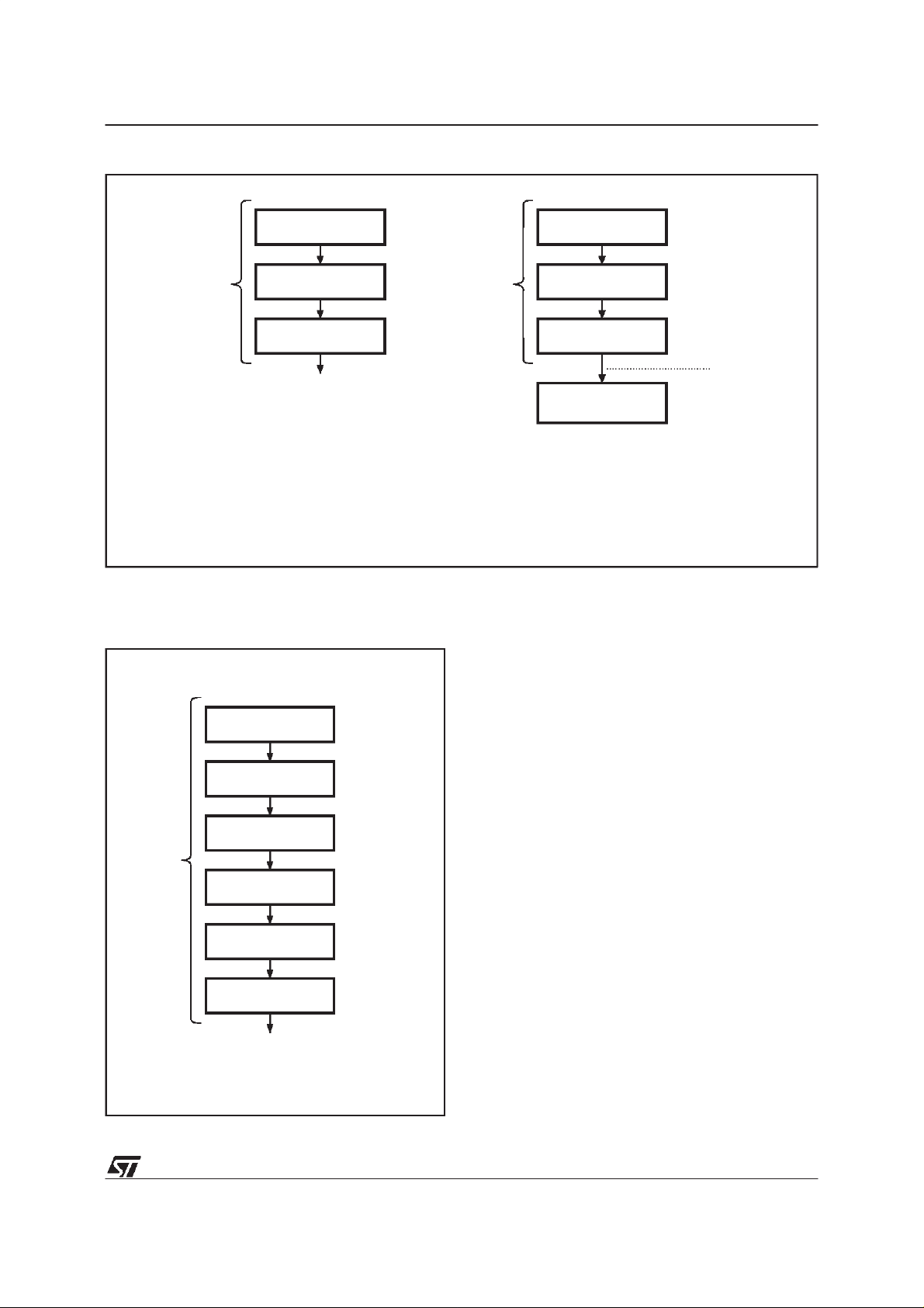
Figure5. Software Data Protection Enable Algorithm and MemoryWrite
M28C16
WRITE AAh in
Address 555h
Page
Write
Instruction
(Note 1)
Note: 1. MSB Address bits (A6 to A10) differ during these specific Page Write operations.
WRITE 55h in
Address 2AAh
WRITE A0h in
Address 555h
SDP is set
SDP ENABLE ALGORITHM
Figure6. Software Data Protection Disable
Algorithm
Page
Write
Instruction
(Note 1)
SoftwareData Protection
The M28C16 offers a software controlled write
protection facility that allows the user to inhibitall
write modesto the device includingthe ChipErase
instruction. This can be useful in protecting the
WRITE AAh in
Address 555h
memory from inadvertent write cycles that may
occurdue touncontrolledbus conditions.
The M28C16is shipped asstandard in the ”unpro-
WRITE 55h in
Address 2AAh
tected” state meaning that the memory contents
can be changed as required by the user. After the
Software Data Protection enable algorithm is issued, the device enters the ”Protect Mode” of
Page
Write
Instruction
WRITE 80h in
Address 555h
WRITE AAh in
Address 555h
operation where no furtherwrite commands have
any effect on the memory contents. The device
remains in this mode until a valid Software Data
Protection (SDP) disable sequence is received
whereby the device reverts to its ”unprotected”
state. The Software Data Protection is fully non-
WRITE 55h in
Address 2AAh
volatile and is not changed by power on/off sequences.
To enable the SoftwareData Protection (SDP) the
WRITE 20h in
Address 555h
devicerequirestheusertowrite(withaPageWrite)
three specificdata bytes to threespecific memory
locations as per Figure 5. Similarly to disable the
Software Data Protection the user has to write
Unprotected State
AI01510
specificdata bytesintosixdifferentlocations asper
Figure 6 (with a Page Write).This complexseries
ensures that the user will never enable or disable
the SoftwareData Protectionaccidentally.
WRITE AAh in
Address 555h
WRITE 55h in
Address 2AAh
WRITE A0h in
Address 555h
Write
(1 up to 64 bytes)
WRITE IN
WHEN SDP IS SET
Page
MEMORY
AI01509B
WRITE
is enabled
5/18
M28C16
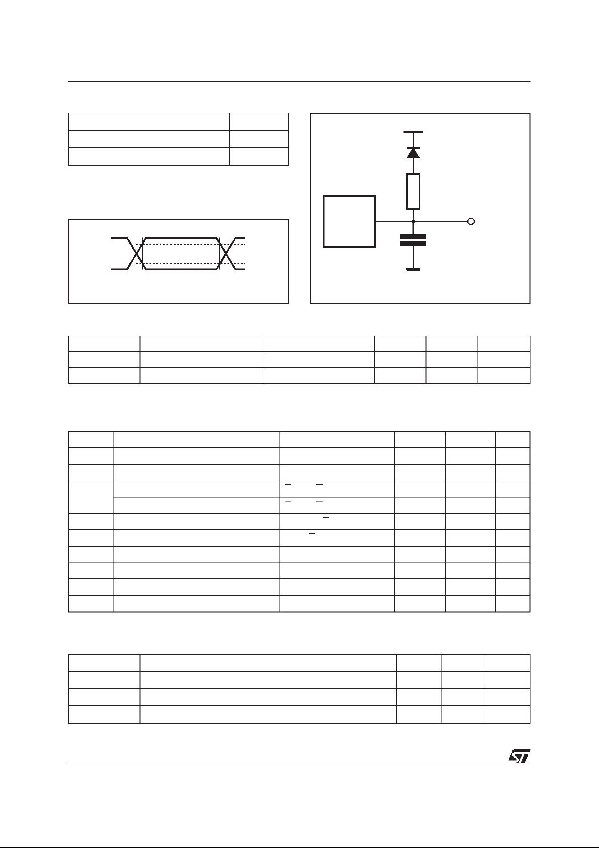
Table 4. AC Measurement Conditions
Input Rise and Fall Times ≤ 20ns
Figure8. AC TestingEquivalentLoad Circuit
1.3V
Input Pulse Voltages 0.4V to 2.4V
Input and Output Timing Ref. Voltages 0.8V to 2.0V
Note that Output Hi-Z is defined as thepoint where data is no
longer driven.
Figure7. AC Testing InputOutput Waveforms
2.4V
0.4V
Table 5. Capacitance
(1)
(TA=25°C, f = 1 MHz )
2.0V
0.8V
AI00826
DEVICE
UNDER
TEST
CLincludes JIG capacitance
1N914
3.3kΩ
CL= 30pF
Symbol Parameter TestCondition Min Max Unit
C
IN
C
OUT
Note: 1. Sampled only, not 100% tested.
Input Capacitance VIN=0V 6 pF
Output Capacitance V
=0V 12 pF
OUT
OUT
AI01129
Table 6. Read Mode DC Characteristics (TA=0 to 70°C or –40 to 85°C; VCC= 4.5V to 5.5V)
Symbol Parameter TestCondition Min Max Unit
I
I
I
CC
I
CC1
I
CC2
V
V
V
V
Note: 1. All I/O’s open circuit.
Table 7. Power Up Timing
Input Leakage Current 0V ≤ VIN≤ V
LI
Output Leakage Current 0V ≤ VIN≤ V
LO
Supply Current (TTL inputs) E = VIL,G=VIL, f = 5 MHz 30 mA
(1)
Supply Current (CMOS inputs) E = V
(1)
Supply Current (Standby) TTL E = V
(1)
Supply Current (Standby) CMOS E > VCC–0.3V 100 µA
Input Low Voltage – 0.3 0.8 V
IL
Input High Voltage 2 VCC+0.5 V
IH
Output Low Voltage IOL= 2.1 mA 0.4 V
OL
Output High Voltage IOH= –400 µA 2.4 V
OH
(1)
(TA=0 to 70°C or –40 to 85°C; VCC= 4.5Vto 5.5V)
,G=VIL, f = 5 MHz 25 mA
IL
CC
CC
IH
Symbol Parameter Min Max Unit
t
PUR
t
PUW
V
WI
Note: 1. Sampled only, not 100% tested.
TimeDelay to Read Operation 1 µs
TimeDelay to Write Operation (once VCC≥ 4.5V) 10 ms
Write Inhibit Threshold 3.0 4.2 V
10 µA
10 µA
1mA
6/18
 Loading...