

SGS Thomson Microelectronics M28256-W, M28256 Datasheet
M28256
256 Kbit (32Kb x8) Parallel EEPROM
with Software Data Protection
PRELIMINARY DATA
January 1999 1/21
Thisis preliminaryinformationon a new product now in developmentor undergoingevaluation.Detail s aresubject to change without notice.
AI01885
15
A0-A14
W
DQ0-DQ7
V
CC
M28256
G
E
V
SS
8
Figure1. LogicDiagram
28
1
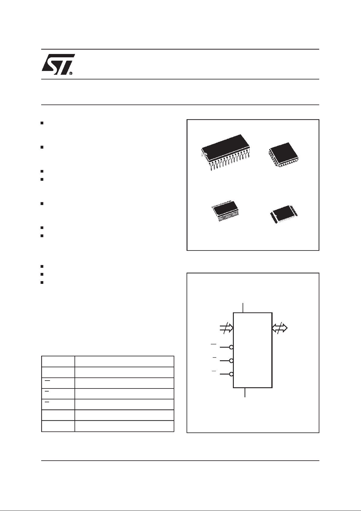
PDIP28 (BS) PLCC32 (KA)
A0-A14 Address Input
DQ0-DQ7 Data Input / Output
W Write Enable
E Chip Enable
G Output Enable
V
CC
Supply Voltage
V
SS
Ground
Table1. Signal Names
FASTACCESSTIME:
– 90ns at 5V
– 120ns at 3V
SINGLESUPPLYVOLTAGE:
–5V±10%for M28256
– 2.7V to 3.6Vfor M28256-xxW
LOWPOWER CONSUMPTION
FASTWRITECYCLE:
– 64 Bytes Page Write Operation
– Byte or Page WriteCycle
ENHANCEDEND of WRITEDETECTION:
– Data Polling
– ToggleBit
STATUSREGISTER
HIGHRELIABILITYDOUBLEPOLYSILICON,
CMOSTECHNOLOGY:
– Endurance >100,000Erase/WriteCycles
– Data Retention>10 Years
JEDECAPPROVEDBYTEWIDE PIN OUT
ADDRESS and DATALATCHEDON-CHIP
SOFTWAREDATAPROTECTION
DESCRIPTION
TheM28256and M28256-Ware 32Kx8lowpower
ParallelEEPROMfabricatedwithSTMicroelectronics proprietary double polysilicon CMOS technology.
TSOP28 (NS)
8 x13.4mm
28
1
SO28 (MS)
300 mils
A1
A0
DQ0
A7
A4
A3
A2
A6
A5
A13
A10
A8
A9
DQ7
W
A11
G
E
DQ5DQ1
DQ2
DQ3V
SS
DQ4
DQ6
A12
A14 V
CC
AI01886
M28256
8
1
2
3
4
5
6
7
9
10
11
12
13
14
16
15
28
27
26
25
24
23
22
21
20
19
18
17
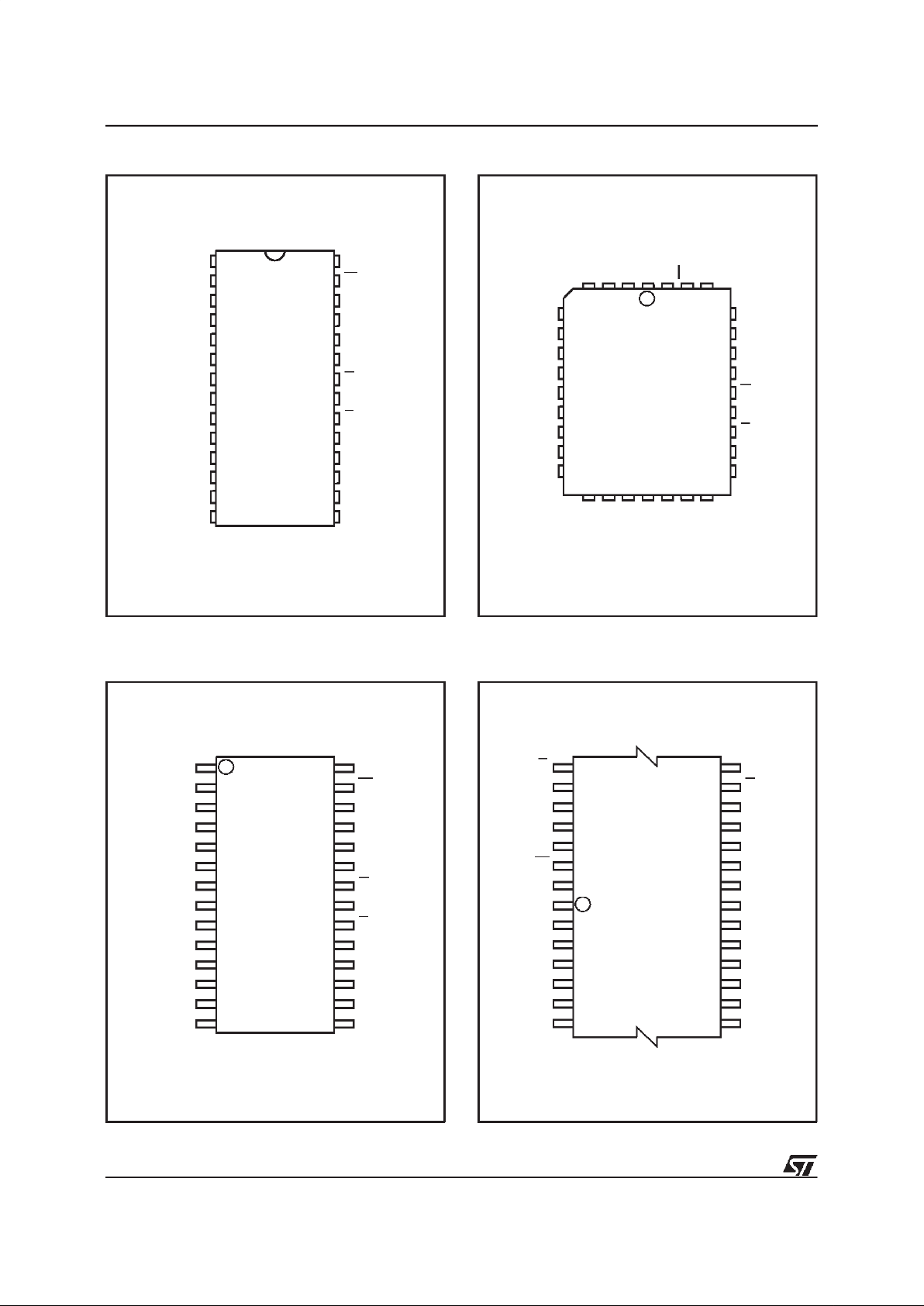
Figure2A. DIPPin Connections
AI01887
A13
A8
A10
DQ4
17
A0
NC
DQ0
DQ1
DQ2DUDQ3
A6
A3
A2
A1
A5
A4
9
W
A9
1
A14
A11
DQ6
A7
DQ7
32
DU
V
CC
M28256
A12
NC
DQ5
G
E
25
V
SS
Figure2B. LCC Pin Connections
Warning:
NC = Not Connected, DU = Don’t Use.
A1
A0
DQ0
A5
A2
A4
A3
A9
A11
DQ7
A8
G
E
DQ5
DQ1
DQ2
DQ3
DQ4
DQ6
A13
W
A12
A6
A14
V
CC
A7
AI01889
M28256
28
1
22
78
14
15
21
V
SS
A10
Figure2D. TSOPPin Connections
DQ0
DQ1
A3
A0
A2
A1
A10
E
A13
DQ7
G
DQ5
V
CC
DQ4
A9
W
A4
A14
A7
AI01888
M28256
8
2
3
4
5
6
7
9
10
11
12
13
14
22
21
20
19
18
17
16
15
DQ2
V
SS
A6
A5
DQ6
28
27
26
25
24
23 A11
DQ3
1
A12
A8
Figure 2C. SOPin Connections
2/21
M28256
Symbol Parameter Value Unit
T
A
Ambient Operating Temperature
(2)
–40to85 °C
T
STG
Storage TemperatureRange – 65 to 150
°
C
V
CC
Supply Voltage – 0.3 to 6.5 V
V
IO
Input/Output Voltage – 0.3 to VCC+0.6 V
V
I
Input Voltage – 0.3 to 6.5 V
V
ESD
Electrostatic Discharge Voltage (Human Body model)
(3)
4000 V
Notes:
1. Except for therating ”Operating Temperature Range”, stresses above those listed in the Table ”Absolute Maximum Ratings”may
cause permanent damage to the device. These are stress ratings only and operation of the device at these or any other conditions
above those indicated in the Operating sections of this specification is not implied.Exposure to Absolute Maximum Rating
conditions for extended periods may affect device reliability.Refer also to the STMicroelectronicsSUREProgram and other
relevant quality documents.
2. Depends on range.
3. 100pF through 1500Ω; MIL-STD-883C, 3015.7
Table2. Absolute Maximum Ratings
(1)
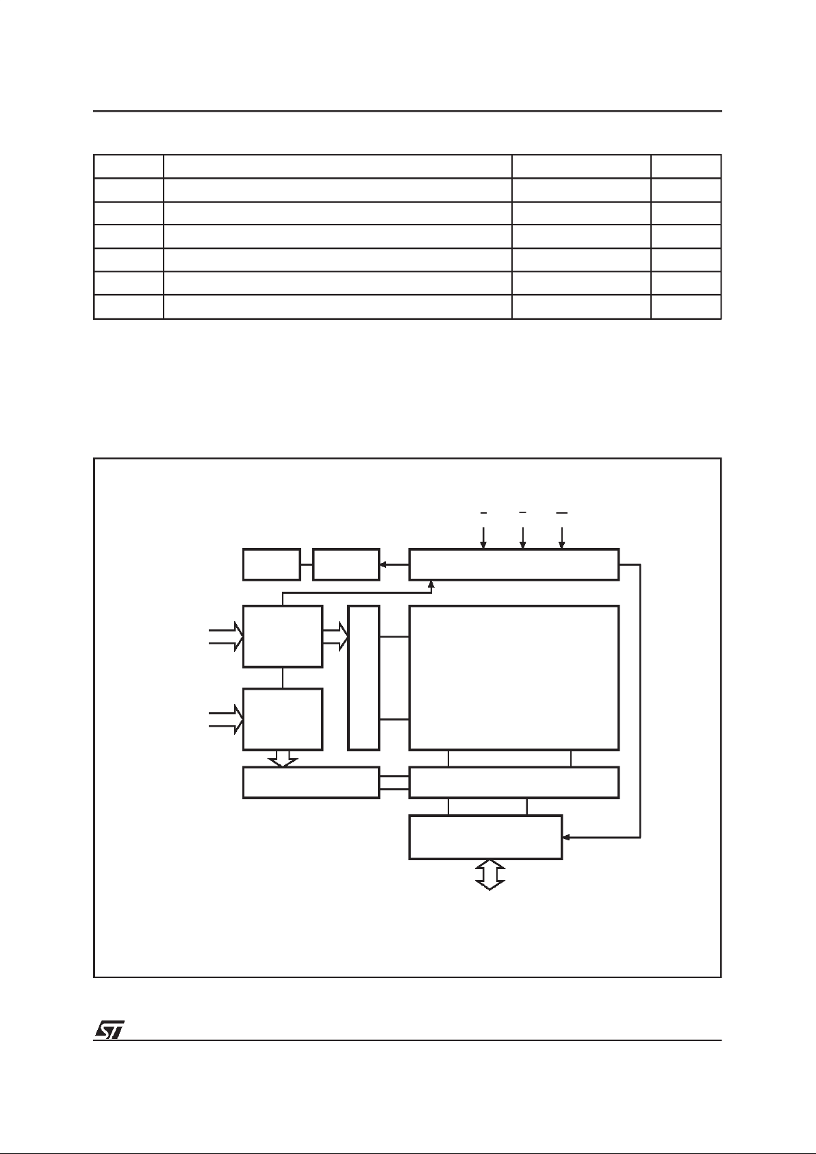
AI01697
ADDRESS
LATCH
A6-A14
(Page Address)
X DECODE
CONTROL LOGIC
256K ARRAY
ADDRESS
LATCH
A0-A5
Y DECODE
VPPGEN RESET
SENSE AND DATA LATCH
I/O BUFFERS
EGW
PAGE
LOAD
TIMER STATUS
TOGGLE BIT
DATA POLLING
DQ0-DQ7
Figure3. Block Diagram
3/21
M28256

Mode E G W DQ0 - DQ7
Read V
IL
V
IL
V
IH
Data Out
Write V
IL
V
IH
V
IL
Data In
Standby / Write Inhibit V
IH
X X Hi-Z
Write Inhibit X X V
IH
Data Out or Hi-Z
Write Inhibit X V
IL
X Data Out or Hi-Z
Output Disable X V
IH
X Hi-Z
Notes: 1. X = VIHor V
IL.
Table3. Operating Modes
(1)
The devices offer fast access timewith low power
dissipationand requires a 5V or 3Vpower supply.
The circuit has been designed to offer a flexible
microcontroller interface featuring both hardware
and software handshaking with Data Polling and
Toggle Bit and access to a status register. The
devicessupport a 64 byte page write operation.A
Software Data Protection (SDP) is also possible
using the standardJEDECalgorithm.
PIN DESCRIPTION
Addresses (A0-A14).
The address inputs select
an 8-bit memory location during a read or write
operation.
Chip Enable (E).
The chip enable input must be
lowto enableall read/writeoperations.When Chip
Enableis high, power consumptionis reduced.
OutputEnable (G).
The Output Enable input controls the dataoutput buffers and is usedto initiate
readoperations.
DataIn/ Out(DQ0-DQ7).
Datais writtento orread
fromthe memorythrough the I/O pins.
WriteEnable(W).
TheWriteEnable inputcontrols
the writingof datato thememory.
OPERATIONS
WriteProtection
In orderto preventdata corruptionand inadvertent
writeoperations;an internalV
CC
comparatorinhib-
its Write operationsif V
CC
is below VWI (see Table
7andTable9).Accesstothememoryinwrite mode
is allowed after a power-upas specifiedin Table7
and Table 9.
Read
Thedevice is accessedlike a staticRAM. WhenE
and G are low with W high, the data addressedis
presented on the I/O pins. The I/O pins are high
impedancewhen either G or E is high.
Write
Writeoperations are initiated when both W and E
are low and G is high.Thedevice supportsboth E
and W controlled write cycles. The Address is
latched by the falling edge of E or W which ever
occurslast and the Data on the risingedge of E or
W which ever occurs first. Once initiated the write
operation is internally timed until completion and
the status of the Data Polling and the Toggle Bit
functions on DQ7 and DQ6 is controlled accordingly.
Page Write
Page write allows up to 64 bytes within the same
page to be consecutivelylatched into the memory
prior to initiating a programming cycle. All bytes
must be located in a single page address, that is
A14-A6 mustbe the same forall bytes;if not,the
Page Write instruction is not executed. The page
writecan be initiatedby any byte write operation.
A page write is composed of successive Write
instructions which have to be sequenced with a
specific period of time between two consecutive
Write instructions, period of time which has to be
smaller than the t
WHWH
value (see Table 12 and
Table13).
If thisperiod of time exceedsthet
WHWH
value, the
internalprogrammingcycle will start.Onceinitiated
thewrite operationis internallytimed until completion and the status of the Data Polling and the
ToggleBit functionson DQ7and DQ6 is controlled
accordingly.
DESCRIPTION
(Cont’d)
4/21
M28256
StatusRegister
Thedevicesprovide severalWriteoperationstatus
flags that can beused to minimize the application
writetime. These signals are available on the I/O
portbits during programming cycleonly.
Data Polling bit (DQ7).
During the internal write
cycle,any attemptto read the last bytewrittenwill
produceon DQ7 the complementary value of the
previously latched bit. Once the write cycle is finished the true logic value appears on DQ7 in the
readcycle.
Toggle bit (DQ6). The devices offer another way
for determining when the internal write cycle is
completed.During theinternal Erase/Write cycle,
DQ6 will toggle from ”0” to ”1” and ”1” to ”0” (the
first read value is ”0”) on subsequent attempts to
read any byte of the memory. When the internal
cycle is completed the toggling will stop and the
data read on DQ7-DQ0is the addressed memory
byte.The deviceisnow accessiblefor a newRead
or Write operation.
PageLoadTimerStatusbit(DQ5).DuringaPage
Writeinstruction,the devicesexpectto receivethe
stream of data with a minimum period of time
between each data byte. This period of time
(t
WHWH
) isdefined by theon-chip Page Loadtimer
whichrunning/overflowstatusis availableonDQ5.
DQ5 Low indicates that the timeris running, DQ5
Highindicatesthe time-outafter which the internal
writecycle will start.
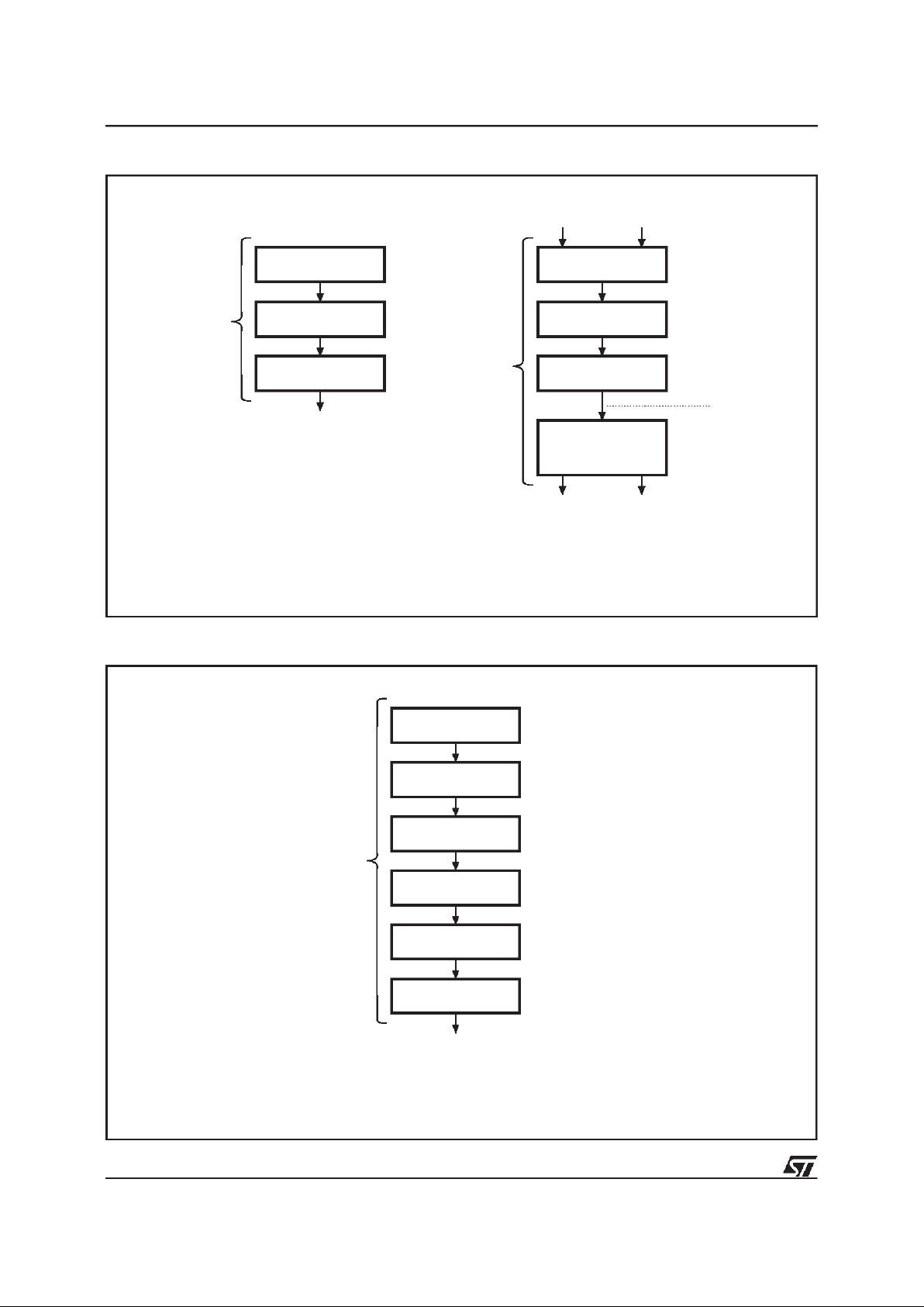
Software Data Protection
The devices offer a software controlled write protectionfacility thatallowstheuser to inhibitallwrite
modesto the device.This can be usefulin protecting the memory from inadvertentwrite cycles that
may occur due to uncontrolledbus conditions.
Thedevicesare shippedas standardinthe”unprotected” state meaning thatthe memory contents
canbe changedas required by the user. After the
Software Data Protection enable algorithm is issued, the device enters the ”Protect Mode” of
operationwhere no further write commands have
anyeffect on the memorycontents.
The devices remain in this mode until a valid
SoftwareData Protection(SDP) disablesequence
is received whereby the device reverts to its ”unprotected”state. TheSoftware Data Protection is
fully non-volatile and is not changed by power
on/off sequences. To enable the Software Data
Protection (SDP) the device requires the user to
write(with a PageWrite addressing three specific
databytestothreespecificmemorylocations,each
locationin a different page) as per Figure 6. Similarly to disable the Software Data Protection the
userhas to write specific data bytes intosix different locations as per Figure 5 (with a Page Write
adressingdifferent bytes in differentpages).
Thiscomplexseriesensuresthattheuserwillnever
enable or disable the Software Data Protection
accidentally.
To write into the devices when SDP is set, the
sequence shown in Figure 6 must be used. This
sequence provides an unlock key to enable the
writeaction, and at the same time SDP continues
to be set.
Anextension to this is whereSDPis required to be
set,and data is to be written.
Using the same sequenceas above, the datacan
be written and SDP is set at the same time, giving
boththese actions in thesame Write cycle (t
WC
).
DQ7 DQ6 DQ5 DQ4 DQ3 DQ2 DQ1 DQ0
DP TB PLTS X X X X X
DP = Data Polling
TB = ToggleBit
PLTS = Page Load Timer Status
Figure4. StatusBit Assignment
5/21
M28256
AI01698B
WRITE AAh in
Address 5555h
WRITE 55h in
Address 2AAAh
WRITE A0h in
Address 5555h
SDP is set
WRITE AAh in
Address 5555h
WRITE 55h in
Address 2AAAh
WRITE A0h in
Address 5555h
WRITE Data
to
be Written in
any Address
SDP ENABLE ALGORITHM
Page
Write
Instruction
Page
Write
Instruction
WRITE
is enabled
SDP
Set
SDP
not Set
Write
in Memory
Write
Data
+
SDP Set
after tWC
Figure5. SoftwareData Protection Enable Algorithmand Memory Write
AI01699B
WRITE AAh in
Address 5555h
WRITE 55h in
Address 2AAAh
WRITE 80h in
Address 5555h
Unprotected
State
after
tWC (Write Cycle time)
WRITE AAh in
Address 5555h
WRITE 55h in
Address 2AAAh
WRITE 20h in
Address 5555h
Page
Write
Instruction
Figure6. SoftwareData Protection Disable Algorithm
6/21
M28256
Input Rise and FallTimes ≤ 20ns
Input Pulse Voltages(M28256) 0.4V to 2.4V
Input Pulse Voltages(M28256-W) 0V toV
CC
–0.3V
Input and Output Timing Ref. Voltages(M28256) 0.8V to 2.0V
Input and Output Timing Ref. Voltages(M28256-W) 0.5 V
CC
Table4. AC MeasurementConditions
AI02101B
4.5V to 5.5V Operating Voltage
2.7V to 3.6V Operating Voltage
VCC– 0.3V
0V
0.5 V
CC
2.4V
0.4V
2.0V
0.8V
Figure7. AC TestingInput Output Waveforms
AI02102B
OUT
CL= 100pF
CLincludes JIG capacitance
I
OL
DEVICE
UNDER
TEST
I
OH
Figure8. AC TestingEquivalent LoadCircuit
Symbol Parameter Test Condition Min Max Unit
C
IN
Input Capacitance VIN=0V 6 pF
C
OUT
Output Capacitance V
OUT
=0V 12 pF
Note:
1. Sampled only, not 100% tested.
Table5. Capacitance
(1)
(TA=25°C, f = 1 MHz )
Symbol Parameter TestCondition Min Max Unit
I
LI
Input Leakage Current 0V ≤ VIN≤ V
CC
10 µA
I
LO
Output Leakage Current 0V ≤ VIN≤ V
CC
10 µA
I
CC
(1)
Supply Current (TTLinputs) E = VIL,G=VIL,f=5MHz 30 mA
Supply Current (CMOS inputs) E = V
IL
,G=VIL,f=5MHz 25 mA
I
CC1
(1)
Supply Current (Standby) TTL E = V
IH
1mA
I
CC2
(1)
Supply Current (Standby) CMOS E > VCC–0.3V 100 µA
V
IL
Input Low Voltage – 0.3 0.8 V
V
IH
Input High Voltage 2 VCC+ 0.5 V
V
OL
Output Low Voltage IOL= 2.1 mA 0.4 V
V
OH
Output High Voltage IOH= –400 µA 2.4
Note: 1. All I/O’s open circuit.
Table6. Read Mode DC Characteristicsfor M28256
(T
A
=0 to 70°C or –40 to85°C;VCC= 4.5V to 5.5V)
7/21
M28256
 Loading...