

SGS Thomson Microelectronics M28010-W, M28010 Datasheet
1/23
PRELIMINARY DATA
February 2000
This is preliminary information on a new product now in development or undergoing evaluation. Details are subject to change without notice.
M28010
1 Mbit (128K x 8) Parallel EEPROM
With Software Data Protection
■ Fast Access Time: 100 ns
■ Single Supply Voltage:
– 4.5 V to 5.5 V for M28010
– 2.7 V to 3.6 V for M28010-W
– 1.8 V to 2.4 V for M28010-R
■ Low Power Consumption
■ Fast BYTE and PAGE WRITE (up to 128 Bytes)
■ Enhanced Write Detection and Monitoring:
– Data Polling
– Toggle Bit
– Page Load Timer Status
■ JEDEC Approved Bytewide Pin-Out
■ Software Data Protection
■ Hardware Data Protection
■ Software Chip Erase
■ 100000 Erase/Write Cycles (minimum)
■ Data Retention(minimum): 10 Years
DESCRIPTION
The M28010 devices consist of 128Kx8 bits oflow
power, parallel EEPROM, fabricated with
STMicroelectronics’ proprietary double polysilicon
CMOS technology. The devices offer fast access
time, with low power dissipation, and require a
single voltage supply (5V, 3V or 2V, depending on
the option chosen).
Figure 1. Logic Diagram
AI02221
17
A0-A16
W
DQ0-DQ7
V
CC
M28010
G
E
V
SS
8
Table 1. Signal Names
A0-A16 Address Input
DQ0-DQ7 Data Input / Output
W Write Enable
E Chip Enable
G Output Enable
V
CC
Supply Voltage
V
SS
Ground
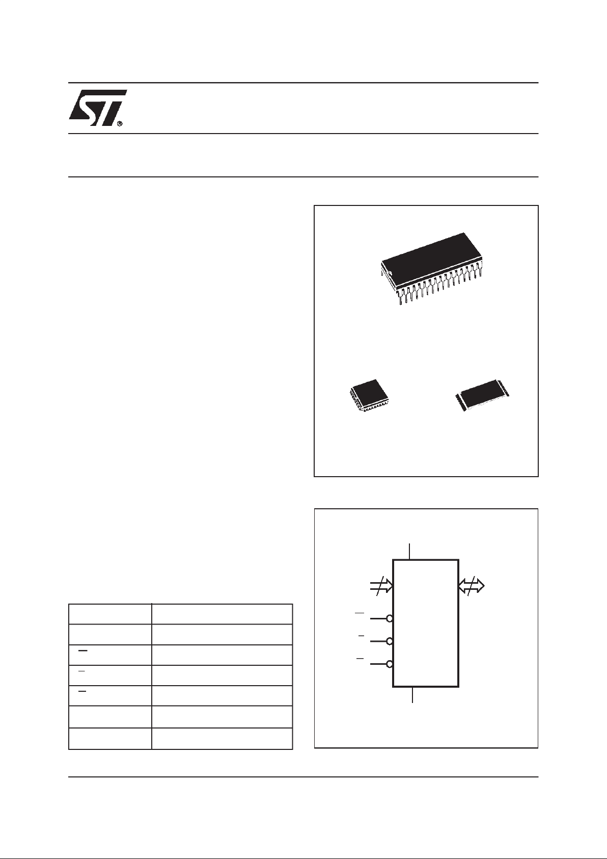
PDIP32 (BA)
PLCC32 (KA)
TSOP32 (NA)
8 x 20 mm
32
1
M28010
2/23
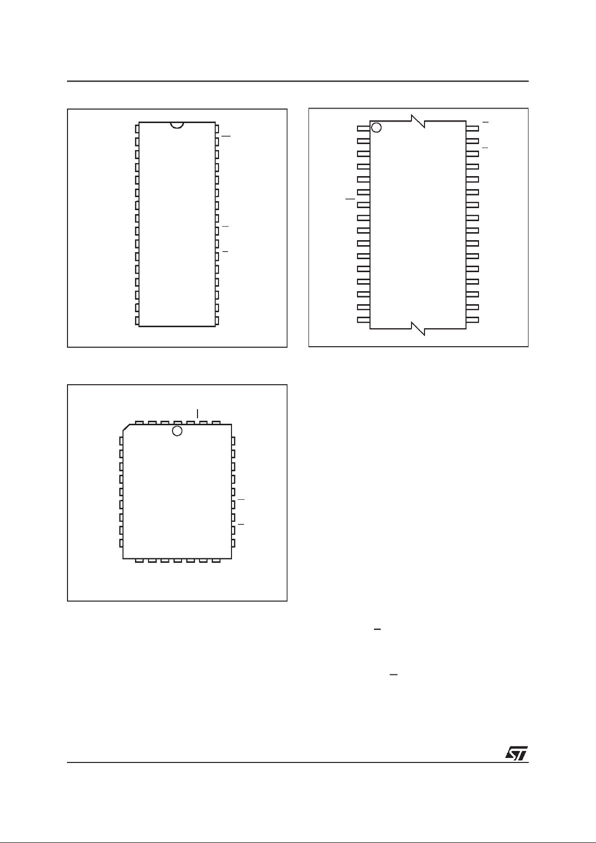
Figure 2A. DIP Connections
Note: 1. DU = Do Not Use
Figure 2B. PLCC Connections
Note: 1. DU = Do Not Use
A1
A0
DQ0
A7
A4
A3
A2
A6
A5
A13
A10
A8
A9
DQ7
A14
A11
G
E
DQ5DQ1
DQ2
DQ3V
SS
DQ4
DQ6
A12
DU V
CC
AI02222
M28010
8
1
15
16
4
5
6
7
9
10
11
12
13
14
32
31
30
27
26
25
24
23
22
21
20
19
18
17
A15 DU
WA16 2
3
29
28
AI02223
DU
A8
A10
DQ4
17
A0
A7
DQ0
DQ1
DQ2
DQ6
DQ3
A6
A3
A2
A1
A5
A4
9
W
A9
1
A16
A11
A14
A12
DQ7
32
DU
V
CC
M28010
A15
A13
DQ5
G
E
25
V
SS
Figure 2C. TSOP Connections
Note: 1. DU = Do Not Use
A2
A1
A0
A6
A3
A5
A4
A9
A11
DQ7
A8
G
E
DQ5
DQ0
DQ1
DQ3
DQ4
DQ6
A13
W
A15
A7
A14
V
CC
A12
AI02224
M28010
8
1
9
16 17
24
25
32
V
SS
A10
DQ2
DU
A16
DU
The device has been designed to offer a flexible
microcontroller interface, featuring both hardware
and software hand-shaking, with Data Polling and
Toggle Bit. The device supports a 128 byte Page
Write operation. Software Data Protection (SDP)
is also supported, using the standard JEDEC
algorithm.
The M28010 is designed for applications requiring
as much as 100,000 write cycles and ten years of
data retention. The organization of the data in a 4
byte (32-bit) “word” format leads to significant
savings in power consumption. Once a byte has
been read, subsequent byte read cycles from the
same “word” (with addresses differing only in the
two least significant bits) are fetched from the
previously loaded Read Buffer, not from the
memoryarray. As aresult, the power consumption
for these subsequent read cycles is much lower
than the power consumption for the first cycle. By
careful design of the memory access patterns, a
50% reduction in the power consumption is
possible.
SIGNAL DESCRIPTION
The external connections to the device are
summarized in Table 1, and their use in Table 3.
Addresses (A0-A16). The address inputs are
used to select one byte from the memory array
during a read or write operation.
Data In/Out (DQ0-DQ7). The contents of the data
byte are written to, or read from, the memory array
through the Data I/O pins.
Chip Enable (E). The chip enable input must be
held low to enable read and write operations.
When Chip Enable is high, power consumption is
reduced.
Output Enable (G). The Output Enable input
controls the data output buffers, and is used to
initiate read operations.
3/23
M28010
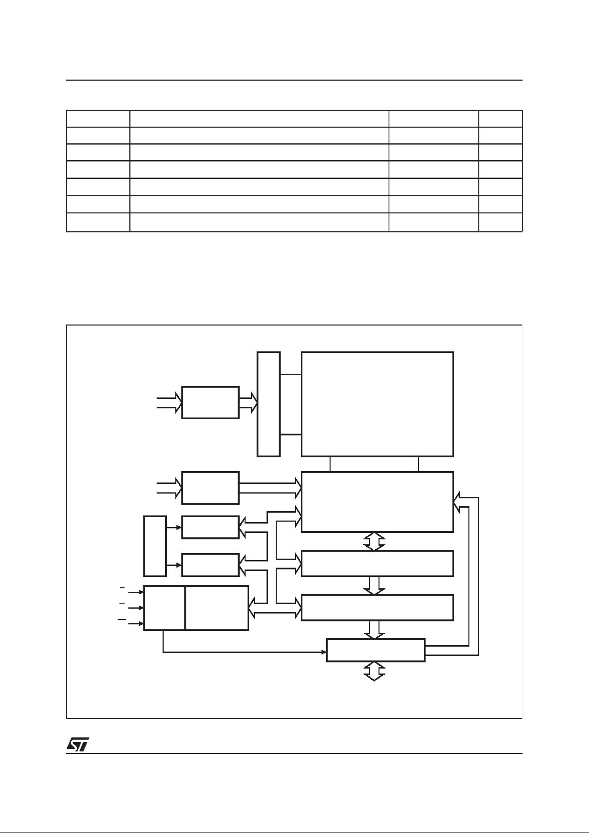
Figure 3. Block Diagram
AI02225
ADDRESS
LATCH
A7-A16
(Page Address)
X DECODE
CONTROL
LOGIC
1Mbit ARRAY
ADDRESS
LATCH
A0-A6
I/O BUFFERS
VPPGEN
LATCH PAGE
Y DECODE
SENSE PAGE & DATA LATCH
E
G
W
DQ0-DQ7
ECC
(1)
& MULTIPLEXER
V
READ
GEN
REFERENCES
PROGRAMMING
STATE
MACHINE
Table 2. Absolute Maximum Ratings
1
Note: 1. Except for the rating “Operating Temperature Range”, stresses above those listed in the Table “Absolute Maximum Ratings” may
cause permanent damage tothe device.These are stress ratings only, and operation of thedevice at these or any other conditions
above those indicated in the Operating sections of this specification is not implied. Exposure to Absolute Maximum Rating conditions forextended periods may affect device reliability. Refer also to the ST SURE Program and other relevant quality documents.
2. MIL-STD-883C, 3015.7 (100 pF, 1500 Ω)
Symbol Parameter Value Unit
T
A
Ambient Operating Temperature –40 to 85 °C
T
STG
Storage Temperature –65 to 150 °C
V
CC
Supply Voltage
–0.3 to V
CCMAX
+1
V
V
IO
Input or Output Voltage (except A9)
–0.3 to V
CC
+0.6
V
V
I
Input Voltage –0.3 to 4.5 V
V
ESD
Electrostatic Discharge Voltage (Human Body model)
2
2000 V
M28010
4/23
Table 3. Operating Modes
1
Note: 1. X = VIHor VIL.
Mode E G W DQ0-DQ7
Read
V
IL
V
IL
V
IH
Data Out
Write V
IL
V
IH
V
IL
Data In
Stand-by / WriteInhibit
V
IH
X X Hi-Z
Write Inhibit X X
V
IH
Data Out or Hi-Z
Write Inhibit X
V
IL
X Data Out or Hi-Z
Output Disable X
V
IH
X Hi-Z
Write Enable(W). TheWrite Enableinput controls
whether the addressedlocation is to be read, from
or written to.
DEVICE OPERATION
In orderto prevent data corruption and inadvertent
write operations, an internal VCCcomparator
inhibits the Write operations if the VCCvoltage is
lower than VWI(see Table 4A to Table 4C). Once
the voltage applied on the VCCpin goes over the
VWIthreshold (VCC>VWI), write access to the
memory is allowed after a time-out t
PUW
,as
specified in Table 4A to Table 4C.
Further protection against data corruption is
offered by the E and Wlow pass filters: any glitch,
on the E andW inputs, witha pulsewidth less than
10 ns (typical) is internally filtered out to prevent
inadvertent write operations to the memory.
Table 4A. Power-Up Timing1for M28010 (5V range)
(TA= –40 to 85 °C; VCC= 4.5 to 5.5 V)
Note: 1. Sampled only, not 100% tested.
Table 4B. Power-Up Timing1for M28010-W (3V range)
(TA= –40 to 85 °C; VCC= 2.7 to 3.6 V)
Note: 1. Sampled only, not 100% tested.
Table 4C. Power-Up Timing1for M28010-R (2V range)
(TA= –40 to 85 °C; VCC= 1.8 to 2.4 V)
Note: 1. Sampled only, not 100% tested.
Symbol Parameter Min. Max. Unit
t
PUR
Time Delay to Read Operation 5 ms
t
PUW
Time Delay to Write Operation (once VCC≥ VWI)
5ms
V
WI
Write Inhibit Threshold 3.0 4.2 V
Symbol Parameter Min. Max. Unit
t
PUR
Time Delay to Read Operation 5 ms
t
PUW
Time Delay to Write Operation (once VCC≥ VWI)5 ms
V
WI
Write Inhibit Threshold 2.0 2.6 V
Symbol Parameter Min. Max. Unit
t
PUR
Time Delay to Read Operation 5 ms
t
PUW
Time Delay to Write Operation (once VCC≥ VWI)5 ms
V
WI
Write Inhibit Threshold 1.2 1.7 V
5/23
M28010
Figure 4. Software Data Protection Enable Algorithms (with or without Memory Write)
Waitfor writecompletion(t
Q5HQ5X
)
Waitfor write completion (t
Q5HQ5X
)
Waitfor write completion (t
Q5HQ5X
)
AI02227B
Write AAh in
Address 5555h
Write 55h in
Address 2AAAh
Write A0h in
Address 5555h
SDP is set
Page Write
Timing
SDP is Disabled and
Application
needs to Enable it, andWrite Data
Time Out (t
WLQ5H
)
DATA has been
written
and SDP is Enabled
SDP is Disabled
and
Application needs to Enable it
Write AAh in
Address 5555h
Write 55h in
Address 2AAAh
Write A0h in
Address 5555h
Page Write
Timing
DATA has been
written
and SDP is Enabled
Time Out (t
WLQ5H
)
Write
data
in any
addresses
within one page
Write
is enabled
Write AAh in
Address 5555h
Write 55h in
Address 2AAAh
Write A0h in
Address 5555h
Page Write
Timing
Time Out (t
WLQ5H
)
Write
data
in any
addresses
within onepage
Write
is enabled
Read
The device is accessed like astatic RAM. When E
and G are low, and W is high, the contents of the
addressed location are presented on the I/O pins.
Otherwise, when either G or E is high, the I/O pins
revert to their high impedance state.
Write
Write operations are initiated when both W and E
are low and G is high. The device supports both
W-controlled and E-controlled write cycles (as
shown inFigure 12 and Figure 13). The address is
latched during the falling edge of W or E (which
ever occurs later) and the data is latched on the
rising edge of W or E (which ever occurs first).
After a delay, t
WLQ5H
, that cannot be shorter than
the value specified in Table 9A to Table 9C, the
internal write cycle starts. It continues, under
internal timing control, until the write operation is
complete. The commencement of this period can
be detected by reading the Page Load Timer
Status on DQ5. The endof the internal write cycle
M28010
6/23
Figure 5. Software Data Protection Disable Algorithms (with or without Memory Write)
Waitforwrite completion (t
Q5HQ5X
)
Waitforwrite completion (t
Q5HQ5X
)
AI02226B
Write AAh in
Address 5555h
Write 55hin
Address 2AAAh
Write 80hin
Address 5555h
SDP is Disabled
Write AAh in
Address 5555h
Write 55hin
Address 2AAAh
Write 20hin
Address 5555h
Page Write
Timing
SDP is Enabled
and
Application needs to Disable it
Time Out (t
WLQ5H
)
Write AAhin
Address 5555h
Write 55h in
Address 2AAAh
Write 80h in
Address 5555h
DATA has been
written
and SDP isDisabled
Write AAhin
Address 5555h
Write 55h in
Address 2AAAh
Write 20h in
Address 5555h
Page Write
Timing
SDP is Enabled
and
Application needs to Write Data
Time Out (t
WLQ5H
)
Write
data
in any
addresses
within onepage
Physical
Write
Instructions
can be detected by reading the status of the Data
Polling and the Toggle Bit functions on DQ7 and
DQ6.
Page Write
The PageWrite mode allows up to 128 bytes to be
written on a single page in a single go. This is
achieved through a series of successive Write
operations, notwo of whichare separatedby more
than the t
WLQ5H
value (as specified in Table 9A to
Table 9C).
The page write can be initiated during any byte
write operation. Following the first Byte Write
instruction, the host may send another address
and data with a minimum data transfer rate of:
1/t
WLQ5H
.
The internal write cycle can start at any instant
after t
WLQ5H
. Once initiated, the write operation is
internally timed, and continues, uninterrupted,
until completion.
All bytes must be located on the same page
address (A16-A7 must be the same for all bytes).
Otherwise, the Page Write operation is not
executed. The Page Write Abort eventis indicated
to the application via DQ1 (as described on page
8).
As with the single byte Write operation, described
above, the DQ5, DQ6 and DQ7 lines can be used
to detect the beginning and end of the internally
controlled phase of the Page Write cycle.
Software Data Protection (SDP)
The device offers a software-controlled writeprotection mechanism that allows the user to
inhibit all write operations to the device, including
chip erase. This can be useful for protecting the
7/23
M28010
memory from inadvertent write cycles that may
occur during periods of instability (uncontrolled
bus conditions when excessive noise is detected,
or when power supply levels are outside their
specified values).
By default, the device is shipped in the
“unprotected” state: the memory contents can be
freely changed by the user. Once the Software
Data Protection Mode is enabled, all write
commands are ignored, and have no effect on the
memory contents.
The device remains in this mode until a valid
Software Data Protection disable sequence is
received. The device reverts to its “unprotected”
state.
The status of the Software Data Protection
(enabled or disabled) is represented by a nonvolatile latch, and is remembered across periods
of the power being off.
The Software Data Protection Enable command
consists of the writing of three specific data bytes
to three specific memory locations (each location
being on a different page), as shown in Figure 4.
Similarly, to disable the Software Data Protection,
the user has to write specific data bytes into six
different locations, as shown in Figure 5. This
complex series of operations protects against the
chance of inadvertent enabling or disabling of the
Software Data Protection mechanism.
When SDP is enabled, the memory array can still
have data written to it, but the sequence is more
complex (and hence better protected from
inadvertent use). The sequence is as shown in
Figure 5. This consists of an unlockkey, to enable
the write action, at the end of which the SDP
continues to be enabled. This allows the SDP to
be enabled, and data to be written, within a single
Write cycle (tWC).
Figure 6. Software Chip Erase Algorithm
Waitfor writecompletion(t
Q5HQ5X
)
AI02236C
Write AAh in
Address 5555h
Write 55h in
Address 2AAAh
Write 80h in
Address 5555h
Whole Array has been Set to FFh
Write AAh in
Address 5555h
Write 55h in
Address 2AAAh
Write 10h in
Address 5555h
Page Write
Timing
Time Out (t
WLQ5H
)
Figure 7. Status Bit Assignment
Figure8.SoftwareData Protection Status Read
Algorithm
AI02486B
DP TB PLTS X X X PWA SDP
DP
TB
PLTS
X
PWA
SDP
DQ7 DQ6 DQ5 DQ4 DQ3 DQ2 DQ1 DQ0
= Data
Polling
= Toggle Bit
= Page Load Timer
Status
=
undefined
= Page Write
Abort
= Software Data Protection
AI02237B
Write AAh in
Address 5555h
Write 55h in
Address 2AAAh
Write 20h in
Address 5555h
Normal UserMode
Read SDP
on DQ0
Write xxh in
Address xxxxh
Page Write
Timing
 Loading...