

SGS Thomson Microelectronics M27V800 Datasheet
Low Voltage UV EPROM and OTP EPROM
■ LOW VOLTAGE READ OPERATION:
3V to3.6V
■ FAST ACCESS TIME: 100ns
■ BYTE-WIDE or WORD-WIDE
CONFIGURABLE
■ 8 Mbit MASK ROMREPLACEMENT
■ LOW POWER CONSUMPTION
– Active Current 30mA at 8MHz
– Standby Current 20µA
■ PROGRAMMING VOLTAGE: 12.5V± 0.25V
■ PROGRAMMING TIME: 100µs/byte (typical)
■ ELECTRONIC SIGNATURE
– Manufacturer Code: 0020h
– Device Code: 00B2h
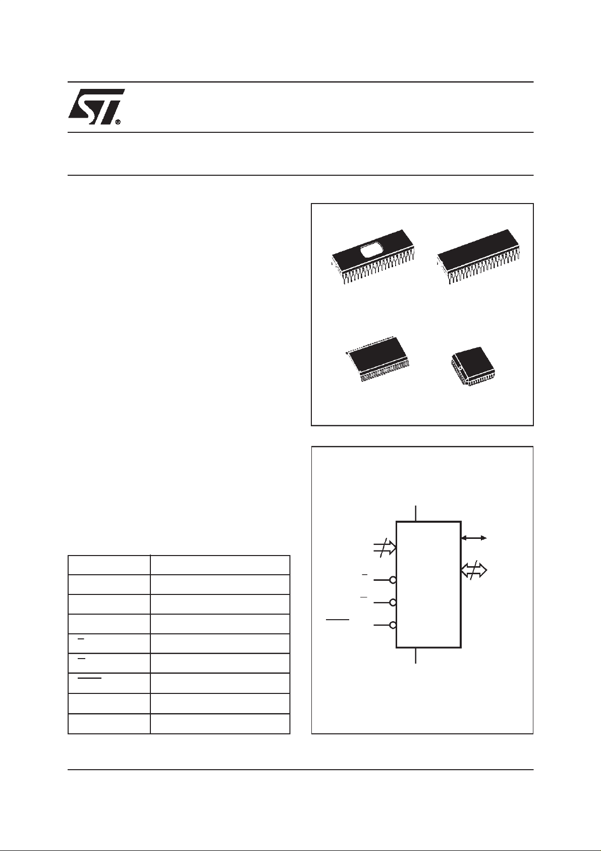
M27V800
8 Mbit (1Mb x8 or 512Kb x16)
42
1
FDIP42W (F) PDIP42 (B)
44
1
SO44 (M) PLCC44 (K)
42
1
DESCRIPTION
The M27V800 is a lowvoltage 8 Mbit EPROM offered inthetwo ranges UV(ultra violet erase) and
OTP (one time programmable). It is ideally suited
for microprocessor systems requiringlarge data or
program storage. It is organised as either 1 Mbit
words of8bit or 512 Kbit words of 16 bit. The pinout is compatible with a 8 Mbit Mask ROM.
Table 1. Signal Names
A0-A18 Address Inputs
Q0-Q7 Data Outputs
Q8-Q14 Data Outputs
Q15A–1 Data Output / Address Input
E Chip Enable
G Output Enable
BYTEV
V
CC
PP
Byte Mode / Program Supply
Supply Voltage
Figure 1. Logic Diagram
V
CC
19
A0-A18
BYTEV
E
G
PP
M27V800
V
SS
Q15A–1
15
Q0-Q14
AI01851
V
SS
Ground
1/16September 1998
M27V800
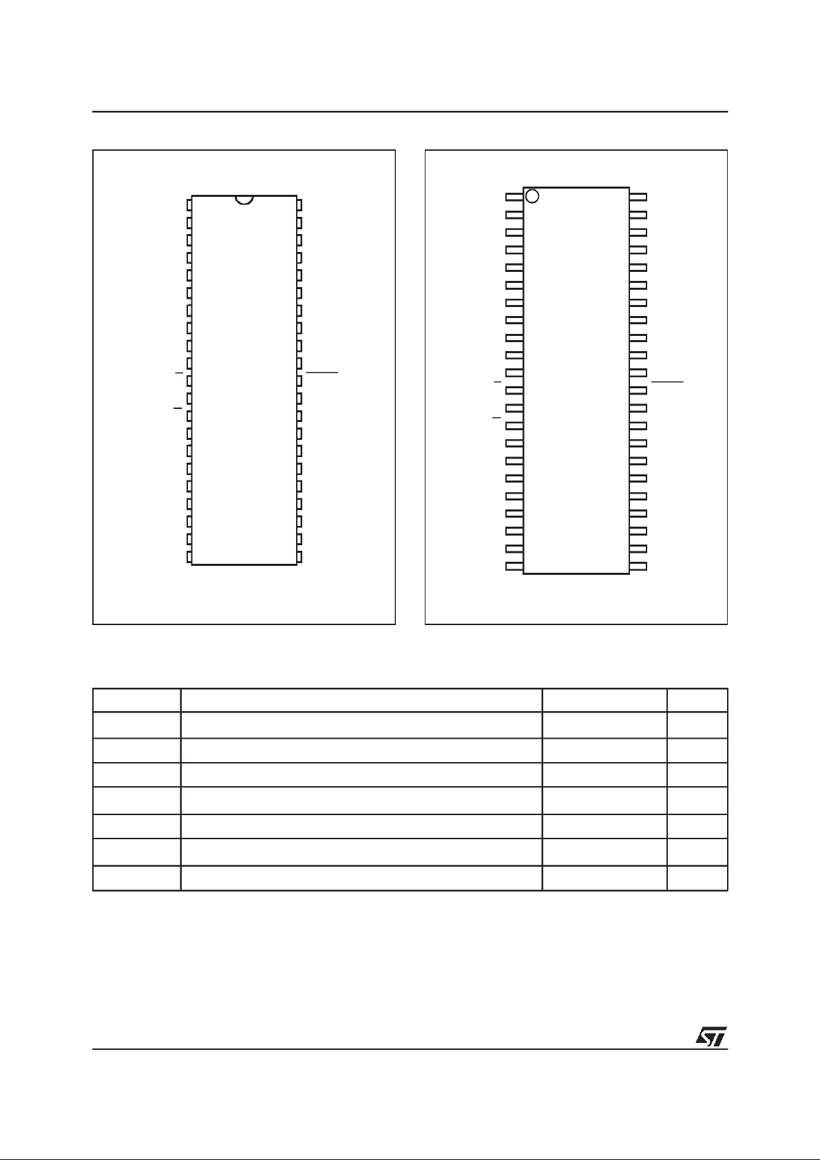
Figure 2A. DIP Pin Connections
A18 NC
A7
A6
A5
A4
A3
A2
A1
A0
V
SS
Q0
Q8
Q1
Q9
Q10
Q3
Q11
1
2
3
4
5
6
7
8
9
10
11
M27V800
E
12
G
13
14
15
16
17
18
19
20
21
42
41
40
39
38
37
36
35
34
33
32
31
30
29
28
27
26
25
24
23
22
AI01852
A8A17
A9
A10
A11
A12
A13
A14
A15
A16
BYTEV
V
SS
Q15A-1
Q7
Q14
Q6
Q13
Q5Q2
Q12
Q4
V
CC
PP
Figure 2B. SO Pin Connections
NC NC
1
2
A17 A8
A7
A6
A5
A4
A3
A2
A1
A0
V
SS
Q0
Q8
3
4
5
6
7
8
9
10
11
12
M27V800
E
13
G
14
15
16
17Q1
Q9
18
19
Q10
Q3
20
21
Q11
44
43
42
41
40
39
38
37
36
35
34
33
32
31
30
29
28
27
26
25
24
2322
AI01853
NCA18
A9
A10
A11
A12
A13
A14
A15
A16
BYTEV
V
SS
Q15A-1
Q7
Q14
Q6
Q13
Q5Q2
Q12
Q4
V
CC
PP
Warning: NC = Not Connected.
Table 2. Absolute Maximum Ratings
Symbol Parameter Value Unit
T
A
T
BIAS
T
STG
(2)
V
IO
V
CC
(2)
V
A9
V
PP
Note: 1. Except for the rating ”Operating Temperature Range”, stresses above thoselisted in the Table ”Absolute Maximum Ratings” may
cause permanent damage to the device. These are stress ratings only and operation of the device at these or any other conditions
above those indicated in the Operating sections of this specification is not implied. Exposure to Absolute Maximum Rating conditions for extended periods may affect device reliability. Refer also to the STMicroelectronics SURE Program and other relevant quality documents.
2. Minimum DC voltage on Input or Output is –0.5V with possible undershoot to –2.0V for a period less than 20ns. Maximum DC
voltage on Output is V
3. Depends on range.
Ambient Operating Temperature
Temperature Under Bias –50 to 125 °C
Storage Temperature –65 to 150 °C
Input or Output Voltage (except A9) –2 to 7 V
Supply Voltage –2 to 7 V
A9 Voltage –2 to 13.5 V
Program Supply Voltage –2 to 14 V
+0.5V with possible overshoot to VCC+2V for a period less than20ns.
CC
(1)
(3)
Warning: NC = Not Connected.
–40 to 125 °C
2/16
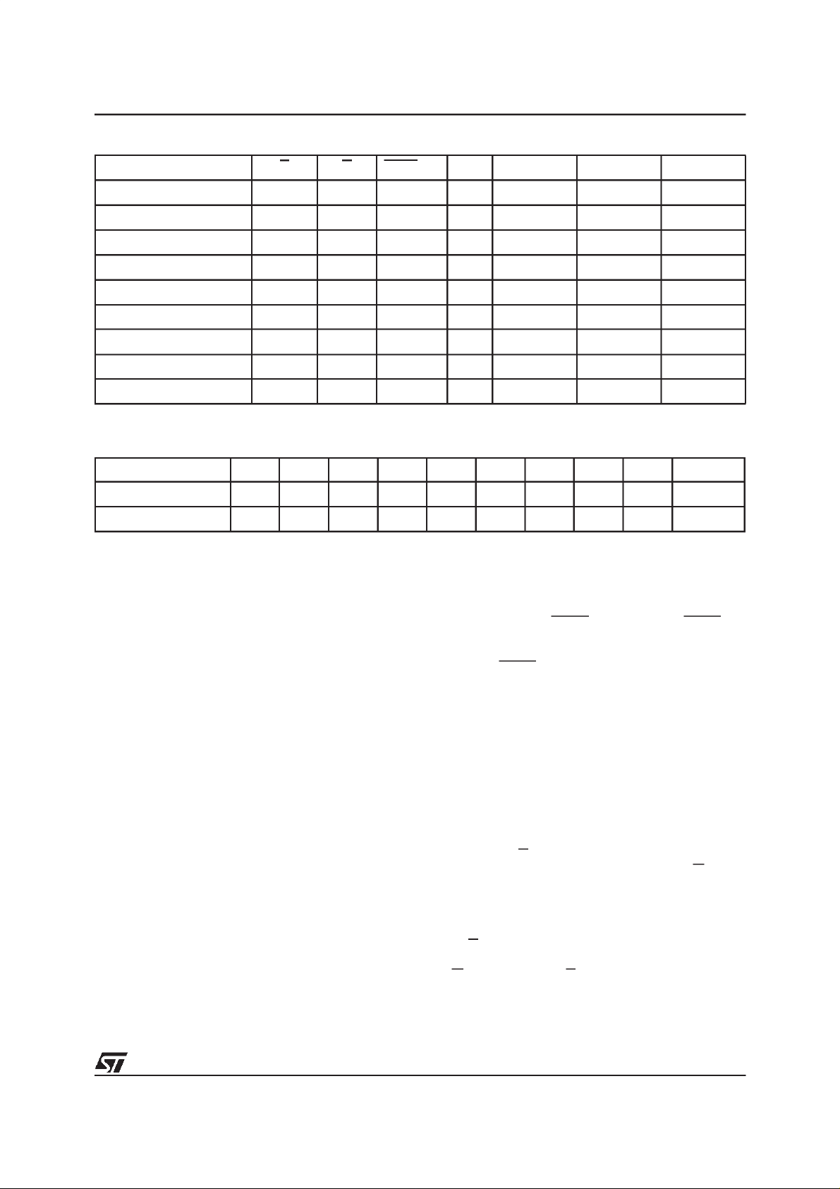
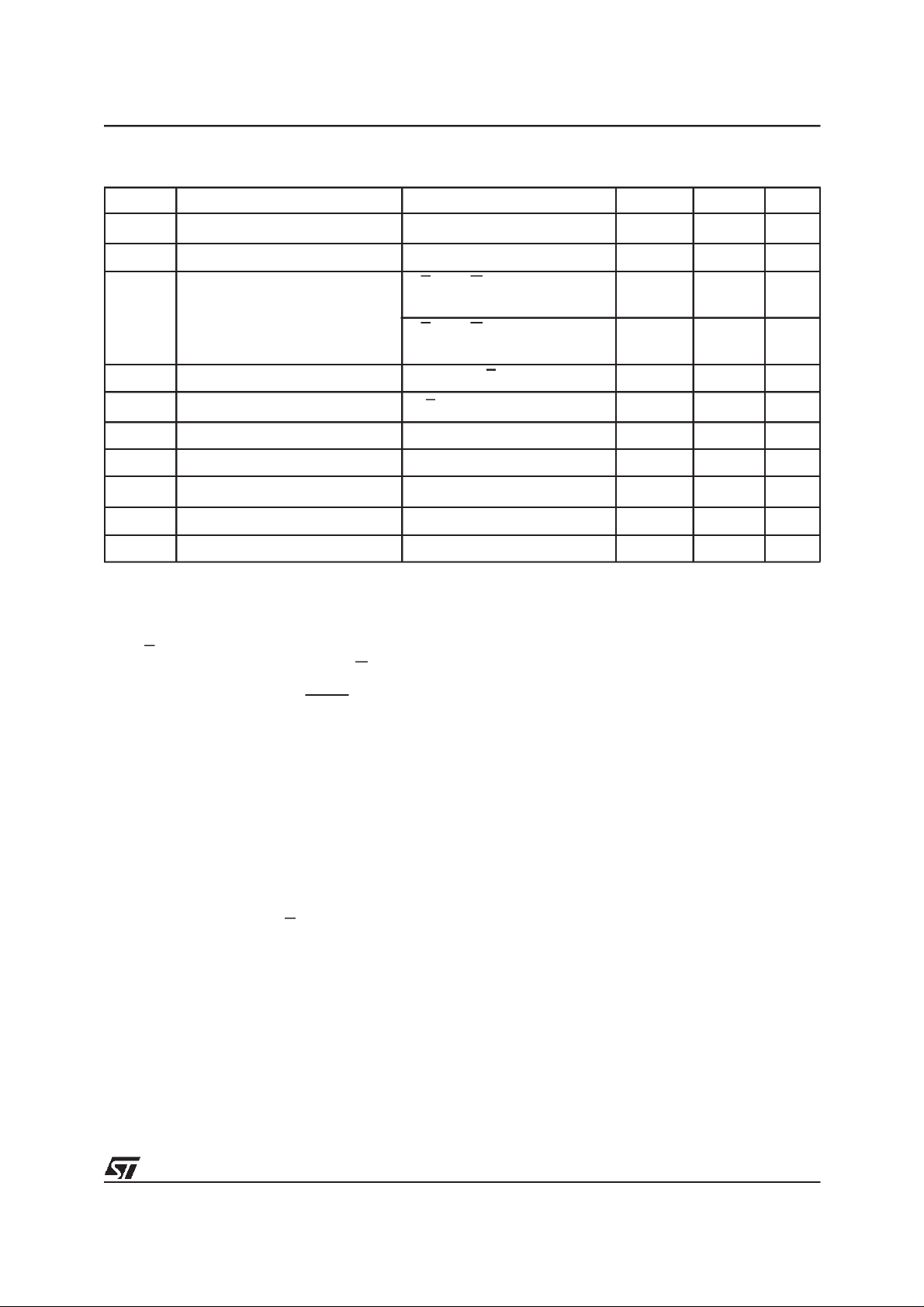
Table 3. Operating Modes
Mode E G BYTEV
Read Word-wide
Read Byte-wide Upper V
Read Byte-wide Lower
Output Disable
Program
Verify
Program Inhibit
Standby
Electronic Signature
Note: X = VIHor VIL,VID= 12V ± 0.5V.
V
IL
V
IL
IL
V
IL
V
IL
Pulse V
V
IH
V
IH
V
IH
V
IL
V
IL
V
IL
V
IL
V
IH
IH
V
IL
V
IH
X X X Hi-Z Hi-Z Hi-Z
V
IL
V
IH
V
IL
V
IL
X X Hi-Z Hi-Z Hi-Z
V
PP
V
PP
V
PP
V
IH
A9 Q0-Q7 Q8-Q14 Q15A–1
PP
X Data Out Data Out Data Out
X Data Out Hi-Z V
X Data Out Hi-Z
X Data In Data In Data In
X Data Out Data Out Data Out
X Hi-Z Hi-Z Hi-Z
V
ID
Codes Codes Code
Table 4. Electronic Signature
Identifier A0 Q7 Q6 Q5 Q4 Q3 Q2 Q1 Q0 Hex Data
M27V800
IH
V
IL
Manufacturer’s Code V
Device Code
Note: Outputs Q8-Q15 are set to ’0’.
IL
V
IH
00100000 20h
10110010 B2h
The M27V800 operates in the read mode with a
supply voltage as low as 3V. The decrease in operating power allows either a reduction of the size
of the battery or an increase in the time between
battery recharges.
The FDIP42W (window ceramic frit-seal package)
has a transparent lid which allows the user to expose the chipto ultraviolet lightto erasethe bit pattern. A new pattern can then be written rapidly to
the device by following the programming procedure.
For applications where the content is programmed
only one time and erasure is not required, the
M27V800 is offered in PDIP42, SO44 and
PLCC44 package.
DEVICE OPERATION
The operating modes ofthe M27V800are listed in
the OperatingModes Table.A single power supply
is required in the read mode. All inputs are TTL
compatible except for VPPand 12V on A9 for the
Electronic Signature.
Read Mode
The M27V800 has two organisations, Word-wide
and Byte-wide.The organisation is selected by the
signal level onthe BYTEVPPpin. When BYTEV
PP
is at VIHthe Word-wide organisation is selected
and the Q15A–1 pin is usedfor Q15 Data Output.
When the BYTEVPPpinis at VILthe Byte-wideorganisation is selected and theQ15A–1 pin is used
for the Address Input A–1. When the memory is
logically regarded as 16 bit wide, but read in the
Byte-wide organisation, then with A–1 at VILthe
lower 8bits of the16bit data are selected and with
A–1 at VIHthe upper 8 bits of the 16 bit data are
selected.
The M27V800 has two control functions, both of
which must be logically active in order to obtain
data at the outputs. In addition the Word-wide or
Byte-wide organisation must be selected.
Chip Enable (E) is thepower control and should be
used fordevice selection. OutputEnable (G)is the
output control and should be used to gate data to
the output pins independent of device selection.
Assuming that the addresses are stable, the address access time (t
from E to output (t
ELQV
output after a delay of t
) is equal to the delay
AVQV
). Data is available at the
from the falling edge
GLQV
of G, assuming that E has been low and the addresseshave been stable forat least t
AVQV-tGLQV
.
3/16
M27V800
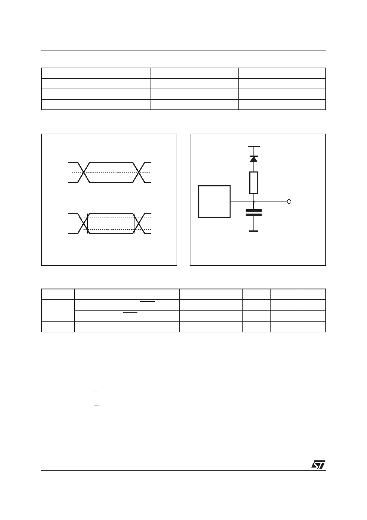
Table 5. AC Measurement Conditions
High Speed Standard
Input Rise and Fall Times ≤ 10ns ≤ 20ns
Input Pulse Voltages 0 to 3V 0.4V to2.4V
Input and Output Timing Ref.Voltages 1.5V 0.8V and 2V
Figure 3. Testing Input Output Waveform
High Speed
3V
1.5V
0V
Standard
2.4V
0.4V
Table 6. Capacitance
(1)
(TA=25°C, f= 1 MHz)
2.0V
0.8V
AI01822
Figure 4. AC Testing Load Circuit
1.3V
1N914
3.3kΩ
DEVICE
UNDER
TEST
C
L
CL= 30pF for HighSpeed
CL= 100pF for Standard
CLincludes JIG capacitance
OUT
AI01823B
Symbol Parameter Test Condition Min Max Unit
C
Input Capacitance (except BYTEVPP)V
IN
C
OUT
Note: Sampled only, not 100% tested.
Input Capacitance (BYTEV
Output Capacitance
)V
PP
=0V
IN
= 0V 120 pF
IN
V
=0V
OUT
10 pF
12 pF
Standby Mode
The M27V800 hasa standby modewhich reduces
the supply current from 20mA to 20µA with low
voltage operationVCC≤ 3.6V, seeRead Mode DC
Characteristics table for details.The M27V800 is
placed in the standby mode by applying a CMOS
high signal to the E input. When in the standby
mode, the outputs are in a high impedance state,
independent of the G input.
4/16
Two Line Output Control
Because EPROMs are usually used in larger
memory arrays, thisproduct features a 2 line control function which accommodates the use of multiple memory connection. The two line control
function allows:
a. the lowest possible memory powerdissipation,
b. complete assurance that output bus contention
will not occur.
M27V800
Table 7. Read Mode DC Characteristics
(1)
(TA= 0 to70 °C; VCC= 3.3V± 10%; VPP=VCC)
Symbol Parameter Test Condition Min Max Unit
I
I
I
CC
I
CC1
I
CC2
I
V
V
IH
V
V
Note: 1. VCCmust be applied simultaneously with or before VPPand removed simultaneously or after VPP.
Input Leakage Current
LI
Output Leakage Current
LO
Supply Current
Supply Current (Standby) TTL
Supply Current (Standby) CMOS
Program Current
PP
Input Low Voltage –0.3 0.8 V
IL
(2)
Input High Voltage 2
Output Low Voltage
OL
Output High VoltageTTL
OH
2. Maximum DC voltage on Output is V
CC
+0.5V.
E=V
IL
f = 8MHz, V
E=V
IL
f = 5MHz, V
E>V
0V ≤ V
0V ≤ V
,G=VIL,I
,G=VIL,I
CC
I
OH
≤ V
IN
CC
≤ V
OUT
E=V
–0.2V,VCC≤ 3.6V
V
PP=VCC
I
= 2.1mA
OL
= –400µA
CC
CC
IH
CC
OUT
≤ 3.6V
OUT
≤ 3.6V
= 0mA,
= 0mA,
2.4 V
±1 µA
±10 µA
30 mA
20 mA
1mA
20 µA
10 µA
V
+1
CC
0.4 V
V
For the most efficient use of these two control
lines, E should be decoded and usedas the primary device selecting function, while G should be
made a common connection to all devices in the
array and connected to the READ line from the
system controlbus. This ensures that alldeselected memory devices are intheir low power standby
mode and that the output pins are only active
when data is required from a particular memory
device.
System Considerations
The power switching characteristics of Advanced
CMOS EPROMsrequire carefull decoupling of the
supplies to the devices. The supply current ICC
has three segments of importance to the system
designer: the standby current, the active current
and the transient peaks that are produced by the
falling andrising edges of E.
The magnitude of the transient current peaks is
dependant on the capacititive and inductive loading of the device outputs. The associatedtransient
voltage peaks can be supressed by complying
with the two line output control and by properly selected decoupling capacitors. It is recommended
that a 0.1µF ceramic capacitor is used on every
device between VCCand VSS. This should be a
high frequency type of low inherent inductance
and should be placed as close as possible to the
device. In addition, a 4.7µF electrolytic capacitor
should be used between VCCand VSSfor every
eight devices. This capacitor should be mounted
near the power supply connection point. The purpose of this capacitor is to overcome the voltage
drop caused by the inductive effects of PCB traces.
5/16
 Loading...