

1/32
NOT FOR NEW DESIGN
February 2002
This is information on a product still in production but not recommended for new designs.
M25P05
512 Kbit, Low Voltage, Serial Flash Memory
With 20 MHz SPI Bus Interface
FEATURES SUMMARY
This device is now designated as “Not for New Design”. Please use the M25P05-A in all future designs (as described in application note AN1511).
■ 512 Kbit of Flash Memory
■ Page Program (up to 128 Bytes) in 3 ms
(typical)
■ Sector Erase (256 Kbit) in 1 s (typical)
■ Bulk Erase (512 Kbit) in 2 s (typical)
■ 2.7 V to 3.6 V Single Supply Voltage
■ SPI Bus Compatible Serial Interface
■ 20 MHz Clock Rate (maximum)
■ Deep Power-down Mode 1 µA (typ ical)
■ Electronic Signature
■ More than 100,000 Erase/Program Cycles per
Sector
■ More than 20 Year Data Retention
Figure 1. Packages
SO8 (MN)
150 mil width
8
1
M25P05
2/32
SUMMARY DESCRIPTION
The M25P05 is a 512 Kbit (64K x 8) Serial Flash
Memory, with advanced write protection mechanisms, accessed by a high spee d SPI-compatible
bus.
The memory can be programmed 1 to 128 bytes at
a time, using the Page Program instruction.
The memory is organized as 2 s ectors, eac h containing 256 pages. E ach page is 128 by tes wide.
Thus, the whole memory can be viewed as consisting of 512 pages, or 65536 bytes.
The whole memory can be eras ed using t he Bulk
Erase instruction, or a sector at a time, us ing the
Sector Erase instruction.
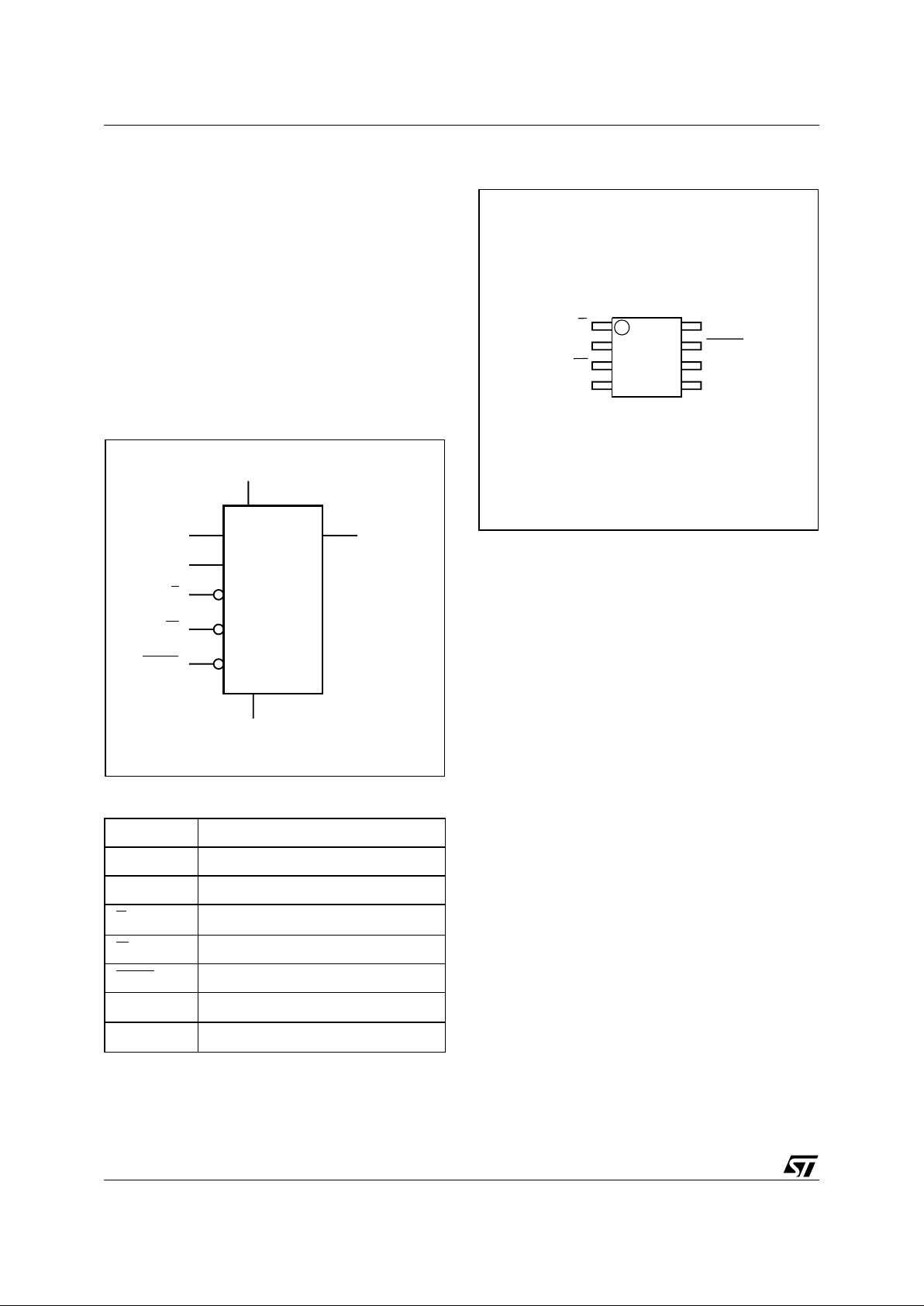
Figure 2. Logic Diagram
Figure 3. SO Connections
Table 1. Signal Names
AI04037
S
V
CC
M25P05
HOLD
V
SS
W
Q
C
D
1
AI04038
2
3
4
8
7
6
5
DV
SS
C
HOLDQ
SV
CC
W
M25P05
C Serial Clock
D Serial Data Input
Q Serial Data Output
S
Chip Select
W
Write Protect
HOLD
Hold
V
CC
Supply Voltage
V
SS
Ground

3/32
M25P05
SIGNAL DESCRIPTION
Serial Data Output (Q). This output signal is
used to transfer data serially out of the device.
Data is shifted out on the falling edge of Serial
Clock (C).
Serial Data Input (D). This input signal is used to
transfer data serially into the device. It receives instructions, addresses, and the data to be programmed. Values are latched on the rising edge of
Serial Clock (C).
Serial Clock (C). This input signal provides the
timing of the serial interface. Instructions, addresses, or data present at Serial Data Input (D) are
latched on the rising edge of Serial Clock (C). Data
on Serial Data Output (Q) changes after the falling
edge of Serial Clock (C).
Chip Select (S
). When this input signal is High,
the device is des elected and Serial Data Output
(Q) is at high impedance. Unless an internal Program, Erase or Write Status Register cycle is in
progress, the device will b e in the Standby m ode
(this is not the Deep Power-down mode). D riving
Chip Selec t ( S
) Low enables the device, placing it
in the active power mode.
After Power-up, a falling edge on Chip Select (S
)
is required prior to the start of any instruction.
Hold (HOLD
). The Hold (HOLD) signal is used to
pause any serial communications with the device
without deselecting the device.
During the Hold condition, the Serial Data Output
(Q) is high impedanc e, and Serial D ata Input (D)
and Serial Clock (C) are Don’t Care.
To start the Hold condition, the device must be se-
lected, wit h C h ip S e lec t (S
) driven Low.
Write Protect (W
). The main purpose of this in-
put signal is to freeze the size of the area of memory that is protected against program or erase
instructions (as specified by the values in the BP1
and BP0 bits of the Status Register).
M25P05
4/32
SPI MODES
These devices can be drive n by a microcont roller
with its SPI periphe ral running in ei the r of the two
following modes:
– CPOL=0, CPHA=0
– CPOL=1, CPHA=1
For these two modes, input dat a is latched in on
the rising edge of Serial Clock (C), and output data
is availa ble from t he falling e dge of Se rial Clock
(C).
The difference between the two modes, as shown
in Figure 5, is the clock polarity when the bus master is in Stand-by mode and not transferring data:
– C remains at 0 for (CPOL=0, CPHA=0)
– C remains at 1 for (CPOL=1, CPHA=1)
Figure 4. Bus Master and Memory Devices on the SPI Bus
Note: 1. T he Write Prot ect (W) a nd Hold (HOLD ) signals s hould be driven, High or Low as appropriate.
Figure 5. SPI Mo de s S upported
AI03746C
Bus Master
(ST6, ST7, ST9,
ST10, Others)
SPI Memory
Device
SDO
SDI
SCK
CQD
S
SPI Memory
Device
CQD
S
SPI Memory
Device
CQD
S
CS3 CS2 CS1
SPI Interface with
(CPOL, CPHA) =
(0, 0) or (1, 1)
W
HOLD
W
HOLD
W
HOLD
AI01438
C
C
MSB LSB
CPHA
D or Q
0
1
CPOL
0
1

5/32
M25P05
OPERATING FEATURES
Page Prog ram m i ng
To program one data byte, two instructions are required: Write Enable (WREN), which is one by te,
and a Page Program (PP) sequence, which consists of four bytes plus data. This is followed by the
internal Program cycle (of duration t
PP
).
To spread this overhead, the Page P rogram (PP)
instruction allows up to 128 bytes to be programmed at a time (changing bits from 1 to 0), provided that they lie in consecutive addresses on the
same page of memory.
Sector Erase and Bulk Erase
The Page Program (PP) instruction allows bits to
be reset from 1 to 0. Before this can be applied, the
bytes of memory need to have been e rased to a ll
1s (FFh). This can be achieved either a sector at a
time, using the Sector Erase (SE) instruction, or
throughout the entire memory, using the Bulk
Erase (BE) instruction.
Polling During a Write, Program or Erase Cycle
A further improvement in the time to Write Status
Register (WRSR), Program (PP) or Erase (SE or
BE) can be achieved by n ot waiting for the worst
case delay (t
W
, tPP, tSE, or tBE). The Write In
Progress (WIP) bit is provided in the Status Register so that the application program can monitor its
value, polling it to establish when the previous
Write cycle, Program cycle or Erase cycle is complete.
Active Power, Stand-by Power and Deep
Power-Down Modes
When Chip Select (S
) is Low, the device is en-
abled, and in the Active Power mode.
When Chip Select (S
) is High, the device is disabled, but could remain in the Active Power mode
until all internal cycles have completed (Program,
Erase, Write Status Register). The device then
goes in to the Stand-by P ower mode. T he device
consumption drops to I
CC1
.
The Deep Power-down mode is entered when the
specific instruction (the Enter Deep Power-down
Mode (DP) instruction) is executed. The device
consumption drops further to I
CC2
. The device remains in this mode until another specific instruction (the Release from Deep Power-down Mode
and Read Electronic S ignature (RE S) instruction)
is executed.
All other instructions are ignored while the device
is in the Deep Power-down mode. This can be
used as an extra software protection mecha nism,
when the device is not in active use, to protect the
device from inadvertant Write, Program or Erase
instructions.
Status Register
The Status Register contains a num ber of status
and control bits, as shown in Table 5, that can be
read or set (as appropriate) by specific instructions.
WIP bit. The Write In Progress (WIP) bit indicates
whether the memory is busy with a Write Sta tus
Register, Program or Erase cycle.
WEL bit. Th e Write Enable Latch (WEL) bit indicates the status of the internal Write Enable Latch.
BP1, BP0 bits. The Block Protect (BP1, BP0) bits
are non-volatile. They define the size of the area to
be software protected against Program and Erase
instructions.
SRWD bit. The Status Register Write Disable
(SRWD) bit is operated in conjunction with the
Write Protect (W
) signal. The Status Register
Write Disable (SRWD) bit an d Write Protect (W
)
signal allow the device to be put in the Hardware
Protected mode. In this mode, the non-volatile bits
of the Status Register (SRWD, BP1, BP0) become
read-only bits.
M25P05
6/32
Table 2. Protected Area Sizes
Protectio n Modes
The environments where non-volatile memory devices are used can be v ery noisy. No SPI device
can operate correctly in the presence of excessive
noise. To help combat this, the M25P05 boasts the
following data protection mechanisms:
■ Power-On Reset and an internal timer (t
PUW
)
can provide protection against inadvertant
changes while the power supply is outside the
operating specification.
■ Program, Erase and Write Status Register
instructions are checked that they consist of a
number of clock pulses that is a multiple of
eight, before they are accepted for execution.
■ All instructions that modify data must be
preceded by a Write Enable (WREN) instruction
to set the Write Enable Latch (WEL) bit . This bit
is returned to its reset state by the following
events:
– Power-up
– Write Disable (WRDI) instruction completion
– Write Status Register (WRSR) instruction
completion
– Page Program (PP) instruction completion
– Sector Erase (SE) instruction completion
– Bulk Erase (BE) instruction completi on
■ The Block Protect (BP1, BP0) bits allow part of
the memory to be configured as read-only. This
is the Software Protected Mode (SPM).
■ The Write Protect (W) signal, in co-operation
with the Status Register Write Disable (SRWD)
bit, allows the Block Protect (BP1, BP0) bits and
Status Register Write Disable (SRWD) bit to be
write-protected. This is the Hardware Protected
Mode (HPM).
■ In addition to the low power consumption
feature, the Deep Power-down mode offers
extra software protection from inadvertant
Write, Program and Erase instructions, as all
instructions are ignored except one particular
instruction (the Release from Deep Powerdown instruction).
Figure 6. Hold Condition Activation
Status Register
Content
Memory Content
BP1 Bit BP0 Bit Protected Area Unprotected Area
0 0 none All sectors (Sectors 0 and 1)
0 1
No protection against Page Program (PP) and Sector Erase (SE)
All sectors (Sectors 0 and 1) protected against Bulk Erase (BE)
1 0
1 1 All sectors (Sectors 0 and 1) none
AI02029C
HOLD
C
Active Hold Active Hold Active

7/32
M25P05
Hold Condition
The Hold (HOLD
) signal is used to pause any serial communications with the device without resetting the clocking sequence. However, taking this
signal Low does not terminate any Write Status
Register, Program or Erase cycle that is currently
in progress.
To enter the Hold condition, the device must be
selected , wit h Ch ip Select (S
) Low.
The Hold condition starts on the falling edge of the
Hold (HOLD
) signal, provided that this coincides
with Serial Clock (C) being L ow (as sh own i n F igure 6).
The Hold condition ends on the rising edge of the
Hold (HOLD
) signal, provided that this coincides
with Serial Clock (C) being Low.
If the falling edge does not coincide with Serial
Clock (C) being Low, the Hold condition starts
when Serial Clock (C) next goes Low. Similarly, if
the rising edge does not coincide with Serial Clock
(C) being Low, the Hold condition ends when Serial Clock (C) next goes Low. (This is shown in Figure 6).
During the Hold condition, the Serial Data Output
(Q) is high impedanc e, and Serial D ata Input (D)
and Serial Clock (C) are Don’t Care.
Normally, the device is kept selected, with Chip
Select (S
) driven Low, for the whole duration of the
Hold condition. This is to en sure that the state of
the internal logic remains unchanged from the moment of entering the Hold condition.
If Chip Select (S
) goes High while the device is in
the Hold condition, this has the effect of reset ting
the internal logic of the device. To restart communication with the device, it is necessary to drive
Hold (HOLD
) High, and then to drive Chip Select
(S
) Low. This prevents the device from going back
to the Hold condition.
M25P05
8/32
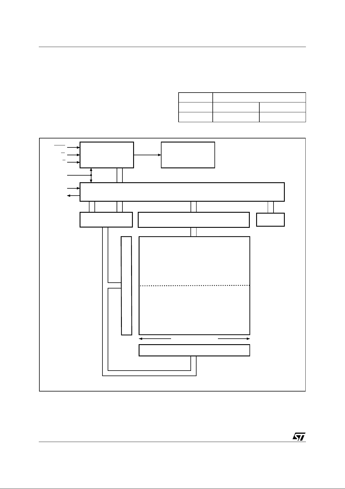
MEMORY OR GANIZATION
The memory is organized as:
■ 65536 bytes (8 bits each)
■ 2 sectors (256 Kbits, 32768 bytes each)
■ 512 pages (128 bytes each).
Each page can be individually programmed (bits
are programmed from 1 to 0). The device is Sector
or Bulk Erasable (bits are erased from 0 to 1) but
not Page Erasable.
Table 3. Memory Organization
Figure 7. Block Diagram
Sector Address Range
1 08000h 0FFFFh
0 00000h 07FFFh
AI04039
HOLD
S
W
Control Logic
High Voltage
Generator
I/O Shift Register
Address Register
and Counter
128 Byte
Data Buffer
128 Bytes (Page Size)
X Decoder
Y Decoder
C
D
Q
Status
Register
00000h
08000h
0FFFFh
0007Fh
9/32
M25P05
INSTRUCTIONS
All instructions, addresses and data are shifted in
and out of the device, most significant bit first.
Serial Data Input (D) is sampled on the first rising
edge of Serial Clock (C) after Chip Select (S
) is
driven Low. Then, the one-byte instruction code
must be shifted in to the device, most significant bit
first, on Serial Data Input (D), each bit being
latched on the rising edges of Serial Clock (C).
The instruction set is listed in Table 4.
Depending on the instruction, the one-byte in-
struction code is follo wed by address bytes, o r by
data bytes, or by both or none. Chip Select (S
)
must be driven High after the last bit of the instruction sequence has been shifted in.
At the end of a Page P rogram (PP), Se ctor Eras e
(SE), Bulk Erase (BE) or Write Status Register
(WRSR) instruction, Chip Select (S
) must be driven High exactly at a byte boundary, otherwise the
instruction is rejected, and is not executed. That is,
Chip Select (S
) must driven High when the number
of clock pulses after Chip Select (S
) being driven
Low is an exact multiple of eight.
All attempts to acc ess t he m em ory array du ring a
Write Status Register cycle, Program cycle or
Erase cycle are ignored, and the internal Write
Status Register cycle, Program cycle or Erase cycle continues unaffected.
Table 4. Instruction Set
Instruction Description One-byte Instruction Code
WREN Write Enable 0000 0110
WRDI Write Disable 0000 0100
RDSR Read Status Register 0000 0101
WRSR Write Status Register 0000 0001
READ Read Data Bytes 0000 0011
PP Page Program 0000 0010
SE Sector Erase 1101 1000
BE Bulk Erase 1100 0111
DP Deep Power-down 1011 1001
RES Release from Deep Power-down, and Read Electronic Signature 1010 1011

M25P05
10/32
Figure 8. Write Enable (WREN) Sequence
Write Enable (WREN)
The Write Enable (WREN) instruction (Fig ure 8)
sets the Write Enable Latch (WEL) bit.
The Write Enable Latch (WEL) bit must be set prior to every Page Program (PP), Sector Erase
(SE), Bulk Erase (BE) and Write Status Register
(WRSR) instruction.
The Write Enable (WREN) instruction is entered
by driving Chip Select (S
) Low, sending the in-
struction code, and then driving Chip Select (S
)
High.
Figure 9. Write Disable (WRDI) Sequence
Write Disable (WRDI)
The Write Disable (WRDI) instruction (Figure 9)
resets the Write Enable Latch (WEL) bit.
The Write Disable (WRDI) instruction is entered by
driving Chip Select (S
) Low, sending the instruc-
tion code, and then driving Chip Select (S
) High.
The Write Enable Latch (WEL) bit is reset under
the following conditions:
– Power-up
– Write Disable (WRDI) instruction completion
– Write Status Register (WRSR) instruction com-
pletion
– Page Program (PP) instruction completion
– Sector Erase (SE) instruction completion
– Bulk Erase (BE) instruction completion
C
D
AI02281D
S
Q
21 34567
High Impedance
0
Instruction
C
D
AI03750C
S
Q
21 34567
High Impedance
0
Instruction
 Loading...