

SGS Thomson Microelectronics M24M01-V, M24M01-S, M24M01 Datasheet

M24M01
1 Mbit Serial I²C Bus EEPROM
FEATURES SUMMARY
■ 400 kHz High Speed Two Wire I
2
C Serial
Interface
■ Single Supply Voltage:
– 2.7V to 3.6V for M24M01-V
– 1.8V to 3.6V for M24M01-S
■ Write Control Input
■ BYTE and PAGE WRITE (up to 128 Bytes)
■ RANDOM and SEQUENTIAL READ Modes
■ Self-Tim e d P rogrammin g Cyc le
■ Automatic Address Incrementing
■ Enhanced ESD/Latch-Up Behavior
■ More than 100000 Erase/Write Cycles
■ More than 40 Year Data Retention
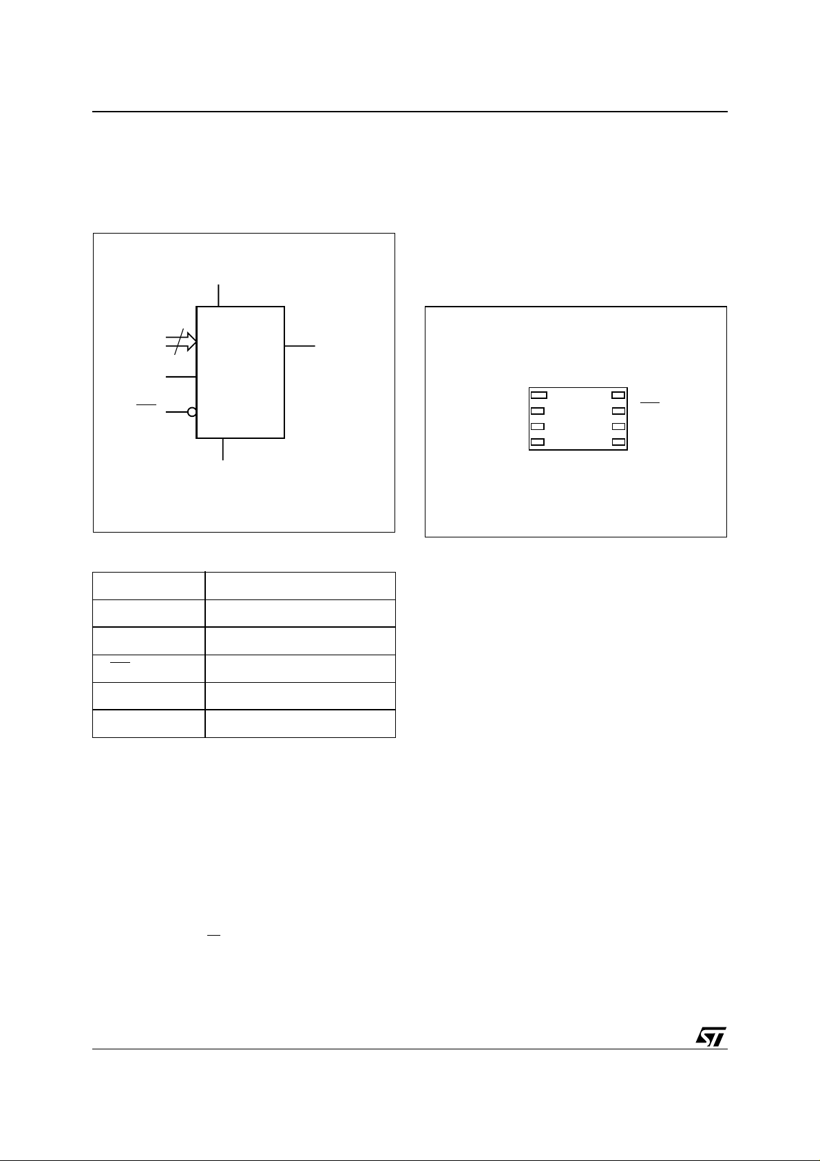
Figure 1. Packages
LGA
LGA8 (LA)
1/19January 2003
M24M01
SUMMARY DESCRIPTION
The M24M01 is a 1 M bit (131, 072 x 8 ) electrically
erasable programmable memory (EEPROM) accessed by an I
Figure 2. Logic Diagram
E1-E2
SCL
WC
2
C-compatible bus .
V
CC
2
M24M01
V
SS
SDA
AI04048B
When writing data to the memory, the device inserts an acknowledge bit during the 9
th
bit time,
following the bus master’s 8-bit transmission.
When data is read by the bus master, the bus
master acknowledges the receipt of the data byte
in the same way. Data transfers are terminated by
a Stop condition after an Ack for Write, and after a
NoAck for Read.
Figure 3. LGA Connections
M24M01
DU
E1
E2
SS
1
2
3
4
8
7
6
5
AI04051C
V
CC
WC
SCL
SDAV
Table 1. Signal Names
E1, E2 Chip Enable
SDA Serial Data
SCL Serial Clock
WC
V
CC
V
SS
These devices are compatible with the I
Write Control
Supply Voltage
Ground
2
C memory protocol. This is a two wire s erial interface that
uses a bi-directional data bus and serial clock. The
devices carry a built-in 4-bit Device Type Identifier
code (1010) in accordance with the I
2
C bus defini-
tion.
The device behaves as a slave in the I
2
C protocol,
with all memory operations synchronized by the
serial clock. Read and Write operations are initiated by a Start condition, generated by the bus master. The Start condition is followed by a Device
Select Code and RW
bit (as described in Table 2),
terminated by an acknowledge bit.
Note: 1. DU = Don’t Us e (should be left unc onnected, or tied to
V
)
SS
Power On Reset: VCC Lock-Out Write Protect
In order to prevent data corruption and inadvertent
Write operations during Power-up, a Power On
Reset (POR) circuit is included. The internal reset
is held active until V
has reached the POR
CC
threshold value, and all operations are disabled –
the device will not respond to any command. In the
same way, when V
drops from the operating
CC
voltage, below the POR threshold value, all operations are disabled and the device will not respond
to any command. A stable and valid V
must be
CC
applied before applying any logic signal.
When the power supply is turned on, V
from V
to VCC(min), passing through a value V
SS
CC
rises
in between. The device ignores all instructions until a time delay of t
ment that V
CC
has elapsed after the mo-
PU
rises above the Vth threshold.
However, the correct operation of the device is not
guaranteed if, by this time, V
V
(min).No instructions should be sent until the
CC
is still below
CC
later of:
–t
afte r VCC passed the Vth threshold
PU
passed the VCC(min) lev el
–V
CC
These values are specified in Table 9.
th
2/19
SIGNAL DESCRIPTION
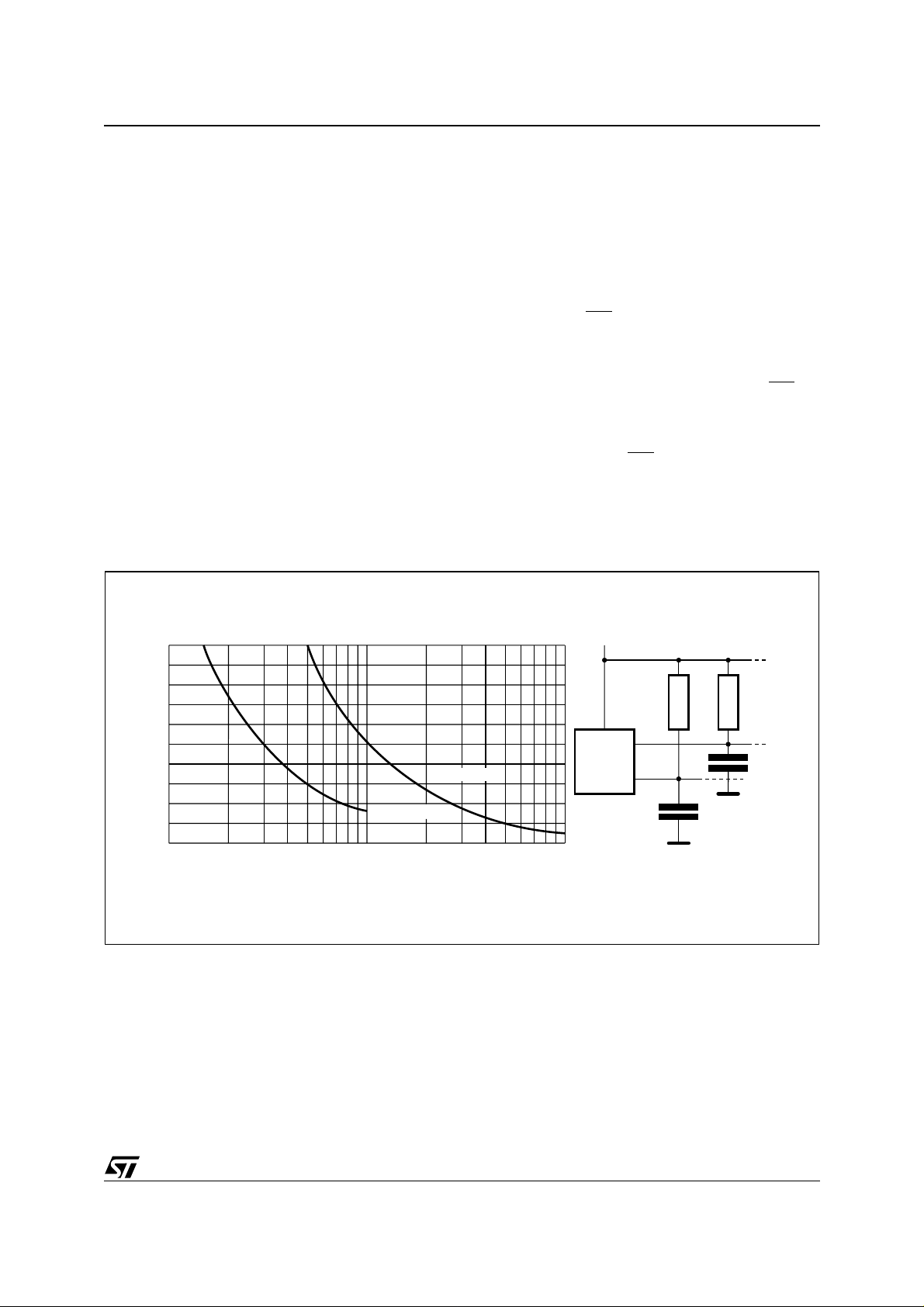
Serial Clock (SCL)
This input signal is used to strobe all data in and
out of the device. In applications where this signal
is used by slave devices to synchronize the bus to
a slower clock, the bus master must have an open
drain output, and a pull-up resistor must be connected from Serial Clock (SCL) to V
. (Figure 4
CC
indicates how the value of the pull-up resist or can
be calculated). In most applications, thoug h, this
method of synchronization is no t employed, and
so the pull-up resistor is not necessary, provided
that the bus maste r has a push-pull (rather than
open drain) output.
Serial Data (SDA)
This bi-directional signal is used to transfer data in
or out of the device. It is an open drain output that
may be wire-OR’ed with other open drain or open
collector signals on the bus. A pull up resistor must
be connected from Serial Data (SDA) to V
CC
. (Figure 4 indicates how the value of the pull-up resistor
can be calculated).
M24M01
Chip Enable (E1, E2)
These input signals are used to set the value that
is to be looked for on bits b3 and b2 of the 7-bit Device Select Code. These inputs must be tied to
or VSS, to establish the Device Select Code.
V
CC
When unconnected, the Chip Enable (E1, E2) signals are internally read as V
11).
Write Control (WC
)
This input signal is useful for protecting the entire
contents of the memory from inadvertent write operations. Write operations are disabled to the entire memory array when Write Control (WC
driven High. When unconnected, the signal is internally read as V
, and Write operations are al-
IL
lowed.
When Write Control (WC
Select and Address bytes are acknowledged,
Data bytes are not acknowledged.
(see Tables 10 and
IL
) is
) is driven High, Device
Figure 4. Maximum R
20
16
12
8
Maximum RP value (kΩ)
4
0
10 1000
Value versus Bus Capacitance (C
L
fc = 100kHz
fc = 400kHz
100
C
(pF)
BUS
) for an I2C Bus
BUS
V
MASTER
CC
SDA
SCL
R
R
C
BUS
L
C
BUS
AI01665
L
3/19
M24M01
DEVICE OPERATION
2
The device supports the I
C protocol. This is summarized in Figure 2. Any device that sends data on
to the bus is defined to be a transmitter, a nd any
device that reads the data to be a receiver. The
device that controls the data transfer is known as
the bus master, and the other as the slave device.
A data transfer can only be initiated by the bus
master, w h ic h will also provide t h e s e r i a l c loc k for
synchronization. The M24M 01 de vice is always a
slave in all communication.
Start Condition
Start is identified by a falling edge of Serial Data
(SDA) while Serial Clock (SCL) is stable in the
High state. A Start condition must precede any
data transfer command. The devi ce continuously
monitors (except duri ng a Write cycle ) Se ri a l Data
(SDA) and Serial Clock (SCL) for a Start condition,
and will not respond unless one is give n.
Stop Condition
Stop is identified by a rising edg e of Serial Data
(SDA) while Serial Clock (SCL) is stable and driven High. A Stop condition terminates communication between the device and the bus master. A
Read command that is followed by NoAck can be
followed by a Stop condi tion to force the device
into the Stand-by mode. A Stop condition at the
end of a Write command triggers the internal EEPROM Wr ite cycle .
Acknowledge Bit (ACK)
The acknowledge bit is used to indicate a successful byte transfer. The bus transmitter, whether it be
bus master or slave device, releases Serial Data
(SDA) after sending eight bits of data. During the
th
clock pulse period, the receiver pulls Serial
9
Data (SDA) Low to acknowledge the receipt of the
eight data bits.
Data Input
During data input, the device samples Serial Data
(SDA) on the rising edge of Serial Clock (SCL).
For correct device operation, Serial Data (SDA)
must be stable during the rising edge of Serial
Clock (SCL), and the Serial Data (SDA) signal
must change
only
when Serial Clock (SCL) is driv-
en Low.
Memory Addressing
To start communication betwee n the bus master
and the slave device, the bus mas ter mus t initiate
a Start condition. Following this, t he bus master
sends the Device Select Code, shown in Tabl e 2
(on Serial Data (SDA), most significant bit first).
The Device Select Code consists of a 4-bit Device
Type Identifier, and a 2-bit Chip Enable “Address”
(E1, E2). To address the memory array, the 4-bit
Device Type Identifier is 1010b.
Up to four memory devices can be connected on a
single I
2
C bus. Each one is given a unique 2-bit
code on the Chip Enable (E1, E2) i nputs. When
the Device Select Code is received on Serial Data
(SDA), the device only responds if the Chip Enable
Address is the same as the value on the Chip Enable (E1, E2) inputs.
th
The 8
bit is the Read/Write bit (RW). This bi t is
set to 1 for Read and 0 for Write operations.
If a match occurs on the Device Select code , the
corresponding device gives an acknowledgment
on Serial Data (SDA) during the 9
th
bit time. If the
device does not match the Device Select code, it
deselects itself from the bus, and goes into Standby mode.
Table 2. Device Select Code
b7 b6 b5 b4 b3 b2 b1 b0
Device Select Code 1 0 1 0 E2 E1 A16 RW
Note: 1. The m ost signific ant bit, b7, is sent first.
4/19
1
Device Type Identifier Chip Enable Address RW
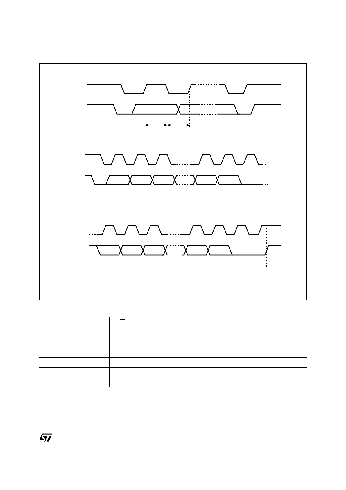
Figure 5. I2C Bus Protocol
SCL
SDA
M24M01
SCL
SDA
SCL
SDA
START
Condition
START
Condition
1 23 789
MSB
1 23 789
MSB ACK
SDA
Input
SDA
Change
STOP
Condition
ACK
STOP
Condition
AI00792B
Table 3. Operating Modes
Mode RW bit
Current Address Read 1 X 1 START, Device Select, RW
0X
Random Address Read
1 X reSTART, Device Select, RW
Sequential Read 1 X
Byte Write 0 V
Page Write 0 V
Note: 1. X = V
IH
or V
.
IL
WC
1
Bytes Initial Sequence
START, Device Select, RW
1
1 Similar to Current or Random Address Read
≥
IL
IL
1 START, Device Select, RW = 0
128 START, Device Select, RW
≤
= 1
= 0, Address
= 1
= 0
5/19
M24M01
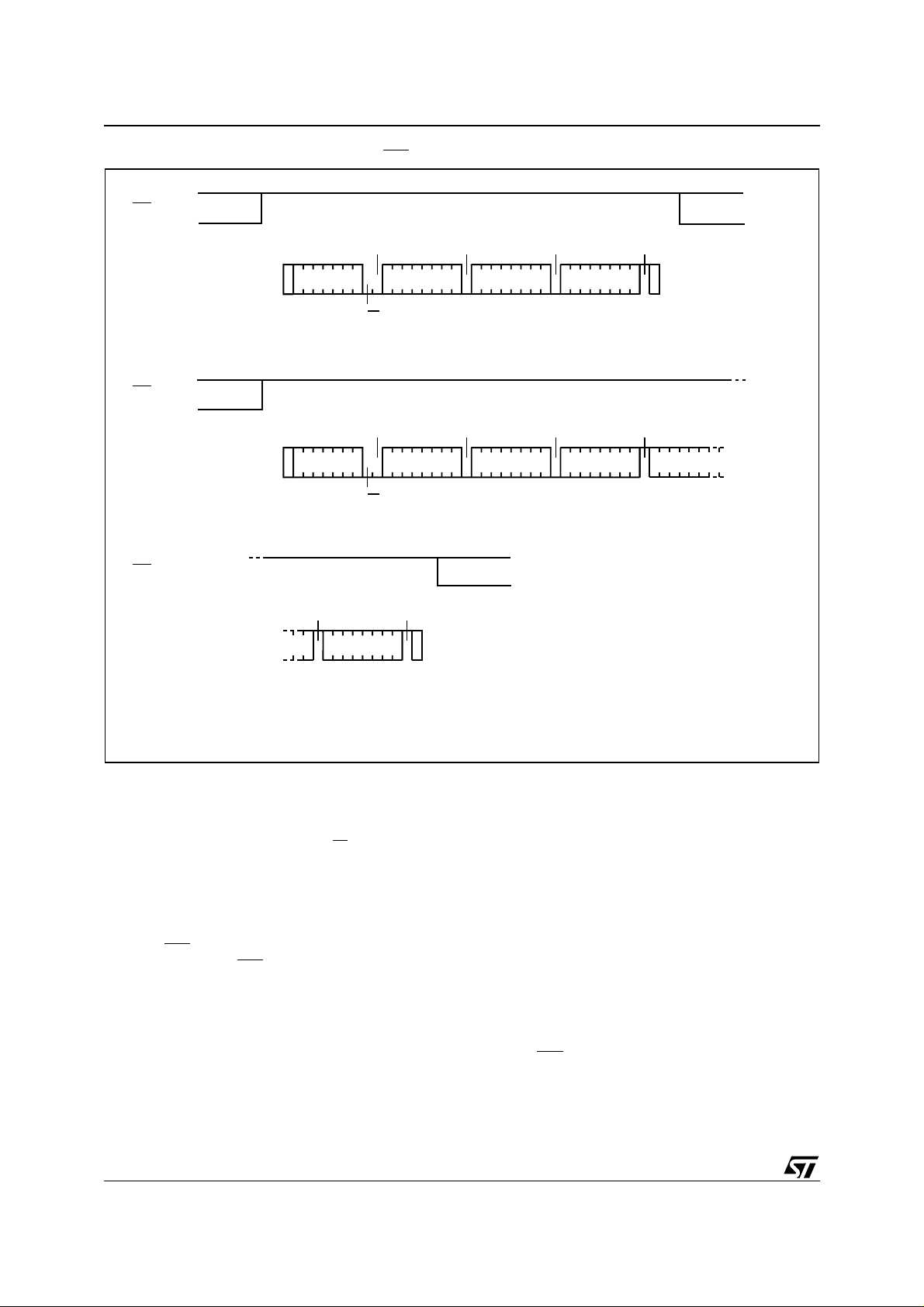
Figure 6. Wri te M ode Sequence s w ith W C =1 (data write inhib i ted)
WC
ACK ACK ACK NO ACK
BYTE WRITE DEV SEL BYTE ADDR BYTE ADDR DATA IN
R/W
START
WC
ACK ACK ACK NO ACK
PAGE WRITE DEV SEL BYTE ADDR
R/W
START
WC (cont'd)
NO ACK NO ACK
PAGE WRITE
(cont'd)
DATA IN N
STOP
BYTE ADDR DATA IN 1
STOP
DATA IN 2
AI01120C
Write Operations
Following a Start condition the bus master sends
a Device Select Code with the RW
bit rese t to 0 .
The device acknowledges this, as shown in Figure
7, and waits for two address bytes. The device responds to each address byte with an acknowledge
bit, and then waits for the data byte.
Writing to the memory may be inhibited if Write
Control (WC
with Write Control (WC
) is driven High. Any Write instruction
) driven High (during a period of time from the Start condition until the end of
the two address bytes) will not modify the memory
contents, and the accompanying data bytes are
not
acknowledged, as shown in Figure 6.
Each data byte in the memory has a 17-bit address. The most significant bit, A16, is sent with
the Device Select Code, and the remaining bits,
A15-A0, in the two a ddress bytes. The Mos t Significant Byte is sent first, followed by the Least Sig-
6/19
nificant Byte. Bits A16 to A0 form t he address of
the byte in memory.
When the bus mast er generates a Stop con dition
immediately after the Ack bi t (in t he “10
th
bit” time
slot), either at the end of a Byte Write or a Page
Write, the internal memory Write cycle is triggered.
A Stop condition at any other time slot does not
trigger the internal Write cycle.
During the internal Write cycle, Serial Da ta (SDA)
is disabled internally, and the devi ce does not respond to any requests.
Byte Write
After the Device Select code and the address
bytes, the bus master sends one dat a byte. If the
addressed location is Write-protected, by Write
Control (WC
) being driven High, the device replies
with NoAck, and the location is not modified. If, instead, the addressed location is not Write-protected, the device replies with Ack. The bus master
 Loading...