

M24C64
M24C32
64Kbit and 32Kbit Serial I²C Bus EEPROM
FEATURES SUMMARY
■ Two Wire I
Supports 400 kHz Protocol
■ Single Supply Voltage:
– 4.5V to 5.5V for M24Cxx
– 2.5V to 5.5V for M24Cxx-W
– 1.8V to 5.5V for M24Cxx-R
■ Write Control Input
■ BYTE and PAGE WRITE (up to 32 Bytes)
■ RANDOM and SEQUENTIAL READ Modes
■ Self-Tim e d P rogramming Cycle
■ Automatic Address Incrementing
■ Enhanced ESD/Latch-Up Behavior
■ More than 1 Million Erase/Write Cycles
■ More than 40 Year Data Retention
2
C Serial Interface
Figure 1. Packages
8
1
PDIP8 (BN)
8
1
SO8 (MN)
150 mil width
TSSOP8 (DW)
169 mil width
1/24May 2003
M24C64, M24C32
SUMMARY DESCRIPTION
2
These I
C-compatible electrically erasable
programmable memory (EEPROM) devices are
organized as 8192 x 8 bits (M24C64) and 4096 x 8
bits (M24C32).
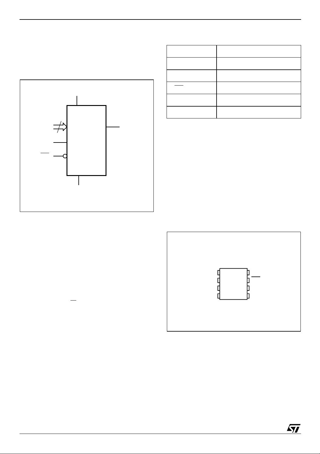
Figure 2. Logic Diagram
V
CC
3
E0-E2 SDA
SCL
WC
M24C64
M24C32
V
SS
AI01844B
Table 1. Signal Names
E0, E1, E2 Chip Enable
SDA Serial Data
SCL Serial Clock
WC
V
CC
V
SS
Power On Reset: V
Write Control
Supply Voltage
Ground
Lock-Out Write Protect
CC
In order to prevent data corruption and inadvertent
Write operations during Power-up, a Power On
Reset (POR) circuit is included. The internal reset
is held active until V
has reached the POR
CC
threshold value, and all operations are disabled –
the device will not respond to any command. In the
same way, when V
drops from the operating
CC
voltage, below the POR threshold value, all operations are disabled and the device will not respond
to any command. A stable and valid V
must be
CC
applied before applying any logic signal.
These devices are compatible with the I
2
C memory protocol. This is a two wire s erial interface that
uses a bi-directional data bus and serial clock. The
devices carry a built-in 4-bit Device Type Identifier
code (1010) in accordance with the I
2
C bus defini-
tion.
The device behaves as a slave in the I
2
C protocol,
with all memory operations synchronized by the
serial clock. Read and Write operations are initiated by a Start condition, generated by the bus master. The Start condition is followed by a Device
Select Code and RW
bit (as described in Table 2),
terminated by an acknowledge bit.
When writing data to the memory, the device in-
serts an acknowledge bit during the 9
th
bit time,
following the bus master’s 8-bit transmission.
When data is read by the bus master, the bus
master acknowledges the receipt of the data byte
in the same way. Data transfers are terminated by
a Stop condition after an Ack for Write, and after a
NoAck for Read.
Figure 3. DIP, SO and TSSOP Connections
M24C64
M24C32
1
E0 V
2
3
E2
4
SS
Note: 1. See page 19 (onwards) for package dimensions, and how
to identify pin-1.
8
7
6
5
AI01845C
CC
WCE1
SCL
SDAV
2/24
SIGNAL DESCRIPTION
Serial Clock (SCL)
This input signal is used to strobe all data in and
out of the device. In applications where this signal
is used by slave devices to synchronize the bus to
a slower clock, the bus master must have an open
drain output, and a pull-up resistor must be connected from Serial Clock (SCL) to V
. (Figure 4
CC
indicates how the value of the pull-up resist or can
be calculated). In most applications, thoug h, this
method of synchronization is no t employed, and
so the pull-up resistor is not necessary, provided
that the bus maste r has a push-pull (rather than
open drain) output.
Serial Data (SDA)
This bi-directional signal is used to transfer data in
or out of the device. It is an open drain output that
may be wire-OR’ed with other open drain or open
collector signals on the bus. A pull up resistor must
be connected from Serial Data (SDA) to V
CC
. (Figure 4 indicates how the value of the pull-up resistor
can be calculated).
M24C64, M24C32
Chip Enable (E0, E1, E2)
These input signals are used to set the value that
is to be looked for on the three least significant bits
(b3, b2, b1) of the 7-bit Device Select Code. These
inputs must be tied to V
Device Select Code.
Write Control (WC
This input signal is useful for protecting the entire
contents of the memory from inadvertent write operations. Write operations are disabled to the entire memory array when Write Control (WC
driven High. When unconnected, the signal is internally read as V
IL
lowed.
When Write Control (WC
Select and Address bytes are acknowledged,
Data bytes are not acknowledged.
or VSS, to establish the
CC
)
) is
, and Write operations are al-
) is driven High, Device
Figure 4. Maximum R
20
16
12
8
Maximum RP value (kΩ)
4
0
10 1000
Value versus Bus Capacitance (C
L
fc = 100kHz
fc = 400kHz
100
C
(pF)
BUS
) for an I2C Bus
BUS
MASTER
V
CC
R
SDA
SCL
R
C
BUS
L
C
BUS
AI01665
L
3/24
M24C64, M24C32
Figure 5. I2C Bus Protocol
SCL
SDA
SCL
SDA
SCL
SDA
START
Condition
START
Condition
1 23 789
MSB
1 23 789
MSB ACK
SDA
Input
SDA
Change
STOP
Condition
ACK
STOP
Condition
AI00792B
Table 2. Device Select Code
Device Type Identifier
1
Chip Enable Address
b7 b6 b5 b4 b3 b2 b1 b0
Device Select Code 1 0 1 0 E2 E1 E0 RW
Note: 1. The most si gnifican t bit, b7, is se nt first.
2. E0 , E 1 and E2 are compared agai nst the respective external pins on the memory device.
2
RW
Table 3. Most Significant Byte Table 4. Least Significant Byte
b15 b14 b13 b12 b11 b10 b9 b8 b7 b6 b5 b4 b3 b2 b1 b0
4/24
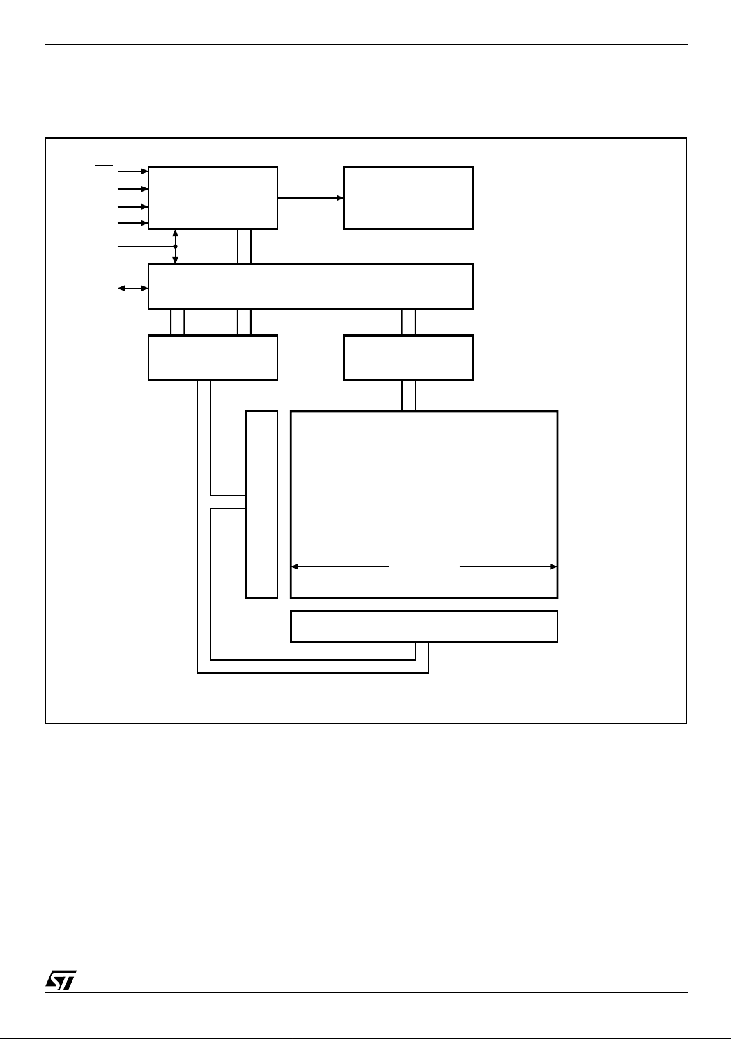
MEMORY ORGANIZATI ON
The memory is organized as shown in Figure 6.
Figure 6. Block Diagram
WC
E0
E1
E2
SCL
Control Logic
M24C64, M24C32
High Voltage
Generator
SDA
Address Register
and Counter
I/O Shift Register
Data
Register
Y Decoder
1 Page
X Decoder
AI06899
5/24
M24C64, M24C32
DEVICE OPERATION
2
The device supports the I
C proto col. This is su m marized in Figure 5. Any device that sends data on
to the bus is defined to be a transmitter, a nd any
device that reads the data to be a receiver. The
device that controls the data transfer is known as
the bus master, and the other as the slave device.
A data transfer can only be initiated by the bus
master, w h ic h will als o provid e t h e s e r i a l c lo c k f or
synchronization. The M24Cxx device is always a
slave in all communication.
Start Condition
Start is identified by a falling edge of Serial Data
(SDA) while Serial Clock (SCL) is stable in the
High state. A Start condition must precede any
data transfer command. The devi ce continuously
monitors (except duri ng a Write cycle ) Se ri a l Data
(SDA) and Serial Clock (SCL) for a Start condition,
and will not respond unless one is give n.
Stop Condition
Stop is identified by a rising edg e of Serial Data
(SDA) while Serial Clock (SCL) is stable and driven High. A Stop condition terminates communication between the device and the bus master. A
Read command that is followed by NoAck can be
followed by a Stop condi tion to force the device
into the Stand-by mode. A Stop condition at the
end of a Write command triggers the internal EEPROM Wr ite cyc le.
Acknowledge Bit (ACK)
The acknowledge bit is used to indicate a successful byte transfer. The bus transmitter, whether it be
bus master or slave device, releases Serial Data
(SDA) after sending eight bits of data. During the
th
clock pulse period, the receiver pulls Serial
9
Data (SDA) Low to acknowledge the receipt of the
eight data bits.
Data Input
During data input, the device samples Serial Data
(SDA) on the rising edge of Serial Clock (SCL).
For correct device operation, Serial Data (SDA)
must be stable during the rising edge of Serial
Clock (SCL), and the Serial Data (SDA) signal
only
must change
when Serial Clock (SCL) is driv-
en Low.
Memory Addressing
To start communication betwee n the bus master
and the slave device, the bus mas ter mus t initiate
a Start condition. Following this, t he bus master
sends the Device Select Code, shown in Tabl e 2
(on Serial Data (SDA), most significant bit first).
The Device Select Code consists of a 4-bit Device
Type Identifier, and a 3-bit Chip Enable “Address”
(E2, E1, E0). To address the memory array, t he 4bit Device Type Identifier is 1010b.
Up to eight memory devices can be connected on
a single I
2
C bus. Each one is given a uniq ue 3-bit
code on the Chip Enable (E0, E1, E2) inputs.
When the Device Select Code is received on Serial Data (SDA), the device only responds if the Chip
Enable Address is the same as the value on the
Chip Enable (E0, E1, E2) inputs.
th
The 8
bit is the Read/Write bit (RW). This bi t is
set to 1 for Read and 0 for Write operations.
If a match occurs on the Device Select code , the
corresponding device gives an acknowledgment
on Serial Data (SDA) during the 9
th
bit time. If the
device does not match the Device Select code, it
deselects itself from the bus, and goes into Standby mode.
Table 5. Operating Modes
Mode RW bit
Current Address Read 1 X 1 START, Device Select, RW
Random Address Read
Sequential Read 1 X
Byte Write 0 V
Page Write 0 V
Note: 1. X = V
6/24
IH
or V
.
IL
0X
1 X reSTART, Device Select, RW
WC
1
IL
IL
Bytes Initial Sequence
1
1 Similar to Current or Random Address Read
≥
1 START, Device Select, RW = 0
32 START, Device Select, RW
≤
START, Device Select, RW
= 1
= 0, Address
= 1
= 0

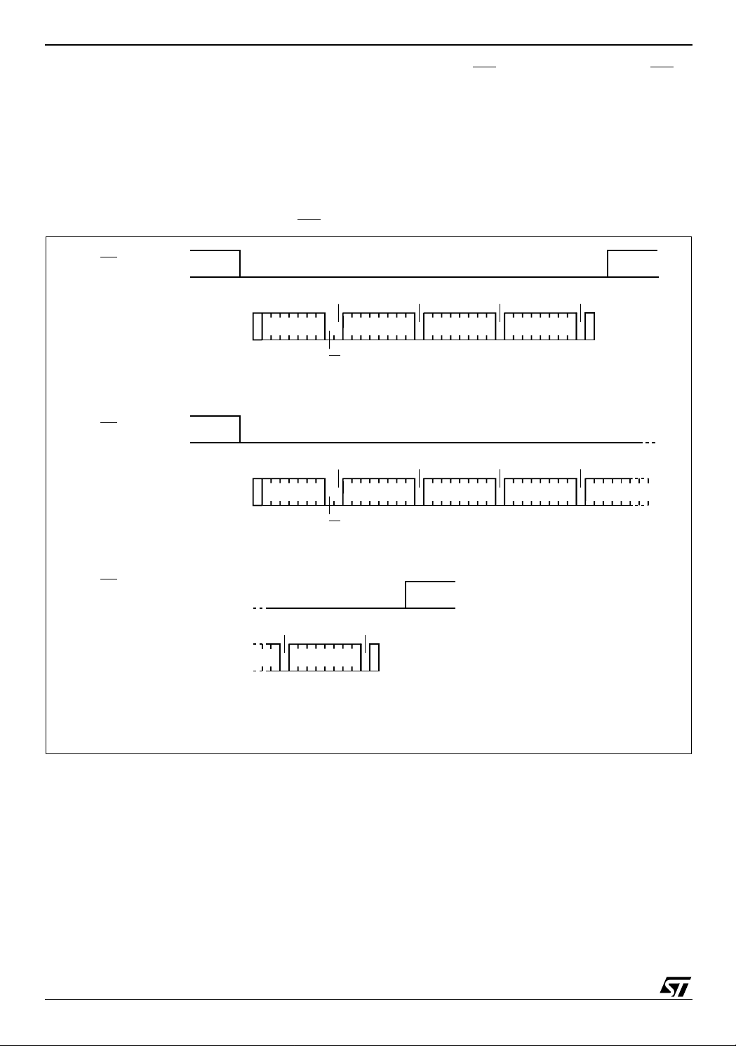
Figure 7. Wri te Mo de S e qu e nces with WC =1 (data wri te inhibi ted)
WC
ACK ACK ACK NO ACK
BYTE WRITE DEV SEL BYTE ADDR BYTE ADDR DATA IN
M24C64, M24C32
R/W
START
WC
ACK ACK ACK NO ACK
PAGE WRITE DEV SEL BYTE ADDR BYTE ADDR DATA IN 1
R/W
START
WC (cont'd)
NO ACK NO ACK
PAGE WRITE
(cont'd)
DATA IN N
STOP
slot), either at the end of a Byte Write or a Page
Write Operations
Following a Start condition the bus master sends
a Device Select Code with the RW
bit rese t to 0 .
The device acknowledges this, as shown in Figure
7, and waits for two address bytes. The device responds to each address byte with an acknowledge
bit, and then waits for the data byte.
Writing to the memory may be inhibited if Write
Control (WC
with Write Control (WC
) is driven High. Any Write instruction
) driven High (during a period of time from the Start condition until the end of
the two address bytes) will not modify the memory
contents, and the accompanying data bytes are
not
acknowledged, as shown in Figure 6.
Each data byte in the m emory has a 16-bit (two
byte wide) address. The Most Significant Byte (Table 3) is sent first, followed by the Least Significant
Byte (Table 4). Bits b15 to b0 form t he add ress of
the byte in memory.
When the bus mast er generates a Stop con dition
immediately after the Ack bi t (in t he “10
th
bit” time
Write, the internal memory Write cycle is triggered.
A Stop condition at any other time slot does not
trigger the internal Write cycle.
During the internal Write cycle, Serial Da ta (SDA)
is disabled internally, and the devi ce does not respond to any requests.
Byte Write
After the Device Select code and the address
bytes, the bus master sends one dat a byte. If the
addressed location is Write-protected, by Write
Control (WC
with NoAck, and the location is not modified. If, instead, the addressed location is not Write-protected, the device replies with Ack. The bus master
terminates the transfer by generating a S top condition, as shown in Figure 7.
Page Write
The Page Write mode allows u p to 32 by tes to be
written in a single Write cycle, provided that they
are all located in the same ’row’ in the memory:
that is, the most significant m emory address bits
STOP
DATA IN 2
AI01120C
) being driven High, the device replies
7/24
M24C64, M24C32
(b12-b5 for M24C64, and b12-b5 for M24C32) are
the same. If more bytes are sent than will fit up to
the end of the row, a condition known as ‘roll-over’
occurs. This should be avoided, as data s tarts to
become overwritten in an implement ation dependent way.
The bus master sends fr om 1 to 32 bytes of data,
each of which is acknowledged by the device if
Figure 8. Wri te Mo de S e qu e nces with W
WC
BYTE WRITE DEV SEL BYTE ADDR BYTE ADDR DATA IN
START
WC
C=0 (data write enabled)
ACK
R/W
ACK ACK ACK ACK
Write Control (WC) is Low. If Write Control (WC) is
High, the contents of the addressed memory location are not modified, and each dat a byte is followed by a NoAck. After each byt e is transferred,
the internal byte address counte r (the 5 least s ignificant address bits only) is incremented. The
transfer is terminated by the bus master generating a Stop condition.
ACK ACK ACK
STOP
PAGE WRITE DEV SEL BYTE ADDR BYTE ADDR DATA IN 1
R/W
START
WC (cont'd)
ACKACK
PAGE WRITE
(cont'd)
DATA IN N
STOP
DATA IN 2
AI01106C
8/24
 Loading...