

LNBS21
LNB SUPPLY AND CONTROL IC WITH
STEP-UP CONVERTER AND I
■ COMPLETE INTERFACE BETWEEN LNB
AND I2CTM BUS
■ BUILT-IN DC/DC CONTROLLER FOR
SINGLE 12V SUPPLY OPERATION
■ ACCURATE BUILT-IN 22KHz TONE
OSCILLATOR
■ SUITS WIDELY ACCEPTED STAND ARDS
■ FAST OSCILLATOR START-UPFACILITATES
DiSEqCTM ENCODING
■ BUILT-IN 22KHz TONE DETECTOR
SUPPORTS BI-DIRECTIONAL DiSEqCTM
■ LOOP-THROUGH FUNCTION FOR SLAVE
OPERATION
■ LNB SHORT CIRCUIT PROTECTION AND
DIAGNOSTIC
■ CABLE LENGTH DIGITAL COMPENSATION
■ INTERNAL OVER TEMPERATURE
PROTECTION
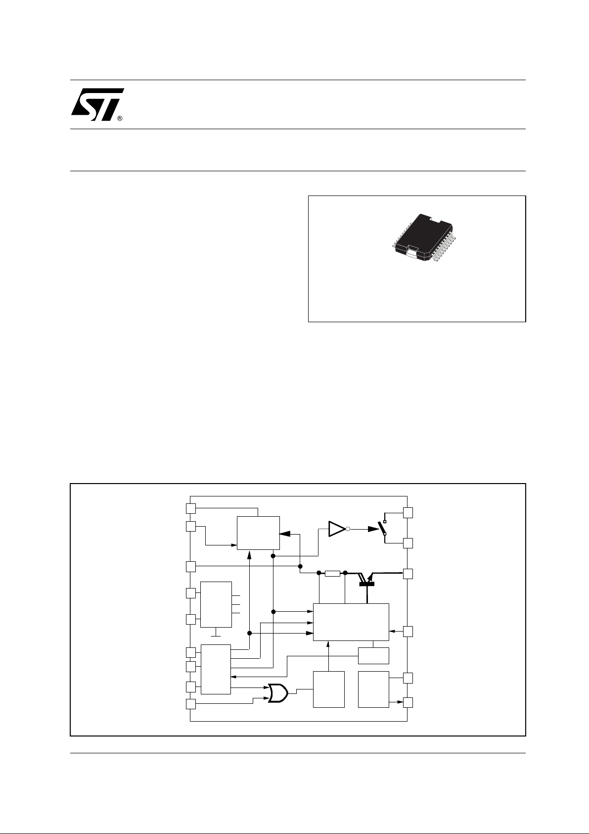
DESCRIPTION
Intended for analog and digital satellite STB
receivers/SatTV, sets/PC cards, the LNBS21 is a
monolithic voltage regulator and interface IC,
2
C INTERFACE
PowerSO-20
assembled in PowerSO-20, specifically designed
to provide the power and the 13/18V, 22KHz tone
signalling to the LNB downconverter in the
antennaortothemultiswitchbox.Inthis
application field, it offers a complete solution with
extremely low component count, low power
dissipation together with simple design and I
2CTM
standard interfacing.
This IC has a built in DC/DC step-up controller
that, from a sing le supply sourc e ranging from 8 to
15V, generates the voltages that let the linear
SCHEMATIC DIAGRAM
Gate
Sense
Vup
Vcc
Byp
SDA
SCL
ADDR
DSQIN
Preregul.+
U.V.lockout
+P.ON res.
I²C
interf.
Step-up
Controller
LNBS21
Feedback
Enable
I Select
V Select
Linear Post-reg
+Modulator
+Protections
22KHz
Oscill.
Diagnostics
Tone
Detector
LT1
LT2
OUT
EXTM
DETIN
DSQOUT
1/19November 2002

LNBS21
post-regulator to work at a minimum dis sipat ed
power. An UnderVoltage Lockout circuit will
disable the whole circuit when the supplied V
CC
drops below a fixedthreshold(6.7V typically). The
internal 22KHz tone generator is factory trimm ed
in accordance to the standards, and can be
controlled either by the I
dedicated pin (DSQIN) that allows immediate
DiSEqC
TM
data encoding (*). All the functions of
this IC are controlled via I
2CTM
2CTM
interface or by a
bus by writing 6
bits on the System Register (SR, 8 bits) . The
same register can be read back, and t wo bits will
report the diagnostic status. When t he IC is put in
Stand-by (EN bit LOW), the power blocks are
disabled and the loop-through switch between
LT1 and LT2 pins is clos ed, thus leaving all LNB
powering and control functions to the Master
Receiver (**). When the regulator blocks are
active (EN bit HIGH), the output can be logic
controlled to be 13 or 18 V (typ.) by mean of t he
VSEL bit (Voltage SELect) for remote controlling
of non-DiSEqC LNBs. Additionally, it is possible
to increment by 1V (typ.) the selected voltage
value to compen sate for the excess v olt age drop
along the coaxial cable (LLC bit HIGH). In order to
minimise t he power dissipation, the output voltage
of the internal step-up converter is adjusted to
allow the linear regulator to work at m inimum
dropout. Another bit of the SR is addressed to the
remote control of non-DiSEqC LNBs: the TEN
(Tone ENable) bit. When it is set to HIGH, a
continuous 22K Hz to ne is gene rated regardless
of the DSQIN pin logic status. The TEN bit must
besetLOWwhentheDSQINpinisusedfor
DiSEqC
DiSEqC
22KHz tone detector. Its input pin (DETIN) must
be AC coupled to the DiSEqC
TM
encoding. The f ully bi-directional
TM
interfacing is completed by the built-in
TM
bus, and the
extractedPWKdataareavailableonthe
DSQOUT pin (*).
In order to improve design flexibility and t o allow
implementation of newcomi ng LNB remote cont ro l
standards, an analogic modulation input pin is
available (EXTM). An appropria te DC blocking
capaci-tor must be used to couple the modulating
signal sour ce to the EX TM pin. When external
modulation is not used, the relevant pin can be left
open.
The cu rrent limitation block has two thresho lds
that can be selected by the I
bitoftheSR;the
SEL
lower threshold is between 650 and 900mA
(I
=HIGH), while the higher threshold is
SEL
between 750 and 1000mA (I
SEL
=LOW).
The current protection block is SOA type. This
limits the short circuit current (Isc) typically at
300mA with I
I
=LOW when the output port is connected to
SEL
=HIGH and at 400mA with
SEL
ground.
It is possible to set the Short Circuit Current
protection either statically (simple current clamp)
or dy-namically by the PCL bit of the SR; when
the PCL (Pulsed Current Limiting) bit is set to
LOW, the overcurrent protection c ircuit w ork s
dynamically: as soon as an overload is detected,
the output is shut-down for a time t
, typically
off
900ms. Sim ult aneously the OLF bit of the System
Register is set to HIGH. After this time has
elapsed, the output is resumed for a time t
10t
(typ.). At the end of ton, if the overload is still
off
on
=1/
detected, the protection circuit will cycle again
through Toff and Ton. At the end of a full Ton in
which no overload is detected, normal operation is
resumed and the OLF bit is reset to LOW. Typical
Ton+Toff time is 990ms and it is determined by an
internal timer. This d yn ami c operation can greatly
reduce the power dissipation in sho rt circuit
condition, still ensuring excellent power-on start
up in most conditions (**) .
However, there could be some cases in which an
highly capacitive load on the ou tput m ay cause a
difficult start-up when the dynamic protection is
chosen. This can be solved by initiating any power
start-up in static mode (PCL=HIGH) and then
switching t o the dynamic mode (PCL=LOW) after
a chosen amount of time. When in static mode,
the OLF bit goes HIGH when the current clamp
limit is reached and returns LOW when the
overload condition is cleared.
This IC is also protect ed against overheating:
when the junction temperature exceeds 150°C
(typ.), the step-up converter and the lin ear
regulator are shut off, the loop-trough switch is
opened, and the OTF bit of the SR is set to HI GH.
Normal operation is resumed and the OTF bit is
reset to LOW when the j unc tion is cooled down to
140°C (typ.).
(*): External components are needed to comply to bi-directional DiSEqCTMbus hardware require-ments. Full compliance of the whole application to DiSEqC
(**): The current limitation circuit has no effect on the loop-through switch. When EN bit is LOW, the current flowing from LT1 to LT2 must
be externally limited.
2/19
TM
specifications is not implied by the use of this IC.
ORDERING CODES
LNBS21
TYPE
PowerSO-20
(Tube)
PowerSO-20
(Tape & Reel)
LNBS21 LNBS21PD LNBS21PD-TR
ABSOLUTE MAXIMUM RATINGS
Symbol Parameter Value Unit
V
V
V
LT1,VLT2
I
V
V
V
DETIN
V
I
V
I
GATE
V
SENSE
V
ADDRESS
T
T
Absolute Maximum Ratings are those values beyond which damage to the device may occur. Functional operation under these condition is
not implied.
DC Input Voltage
CC
DC Input Voltage
UP
DC Input Voltage
Output Current
O
DC Output Pin Voltage
O
Logic Input Voltage (SDA, SCL, DSQIN)
I
Detector Input Signal Amplitude
Logic High Output Voltage (DSQOUT)
OH
Bypass Switch ON Current
LT
Bypass Switch OFF Voltage
LT
Gate Current
Current Sense Voltage
Address Pin Voltage
Storage Temperature Range
stg
Operating Junction Temperature Range
op
16 V
25 V
20 V
Internally Limited mA
-0.3 to 22 V
-0.3 to 7 V
2
V
PP
7V
900 mA
±20 V
±400 mA
-0.3 to 1 V
-0.3 to 7 V
-40 to +150 °C
-40 to +125 °C
THERMAL DATA
Symbol Parameter PowerSO-20 Unit
R
thj-case
Thermal Resistance Junction-case
2 °C/W
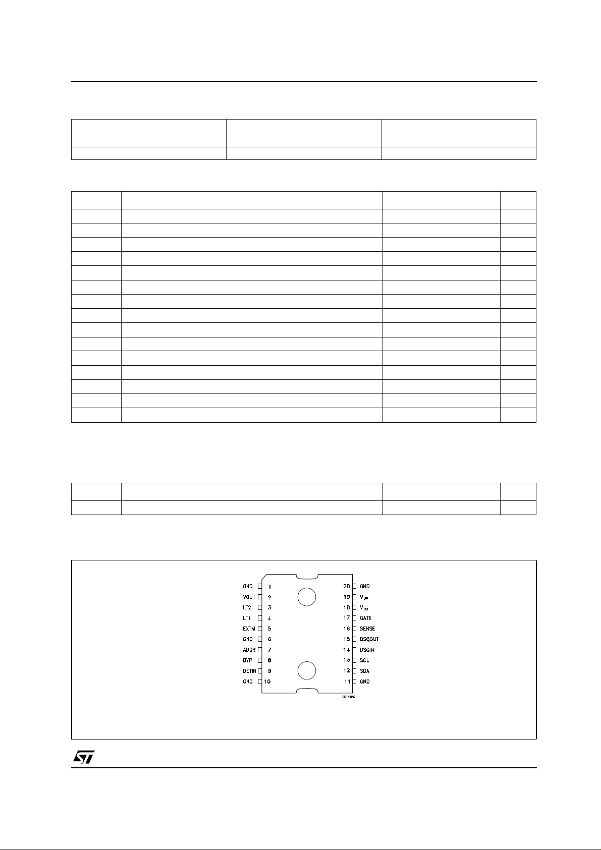
PIN CONFIGUARATION (top view)
PowerSO-20
3/19
LNBS21
TABLE A: PIN CONFIGURATIONS
SYMBOL NAME FUNCTION
V
Supply Input 8V to 15V supply. A 220µF bypass capacitor to
CC
GND with a 470nF (ceramic) in parallel is
PIN NUMBER
vs PACKAGE
recommended
GATE Exrernal Switch Gate External MOS switch Gate connection of the
step-up converter
SENSE Current Sense Input Current Sense comparator input. Connected to
current sensing resistor
V
Step-up Voltage Input of the linear post-regulator. The voltage on this
up
pin is monitored by internal step-ut controller to
keep a minimum dropout across the linear pass
transistor
OUT Output Port Output of the linear post regulator modulator to the
LNB. See truth table for voltage selections.
SDA Serial Data
SCL Serial Clock
Bidirectional data from/to I
Clock from I
2
Cbus.
2
C bus.
DSQIN DiSEqC Input When the TEN bit of the System Register is LOW,
this pin will accept the DiSEqC code from the main
µcontroller. The LNBS21 will use this code to
modulate the internally generated 22kHz carrier. Set
to GND thi pin if not used.
DETIN Detector In 22kHz Tone Detector Input. Must be AC coupled to
the DiSEcQ bus.
DSQOUT DiSEqC Output Open collector output of the tone Detector to the
main µcontroller for DiSEcQ data decoding. It is
LOW when tone is detected.
EXTM Extrernal Modulator External Modulation Input. Need DC decoupling to
the AC source. If not used, can be left open.
GND Ground Circuit Ground. It is internally connected to the die
frame for heat dissipation.
BYP Bypass Capacitor Needed for internal preregulator filtering 8
LT1 Loop Through Switch In standby mode the power switch between LT1
and LT2 is closed. Max allowed current is 900mA.
this pin can be left open if loopthrough function is
not needed.
LT2 Loop Through Switch Same as above 3
ADDR Address Setting
2
C bus addresses available by setting the
Four I
Address Pin level voltage
18
17
16
19
2
12
13
14
9
15
5
1, 10, 11, 20
4
7
4/19
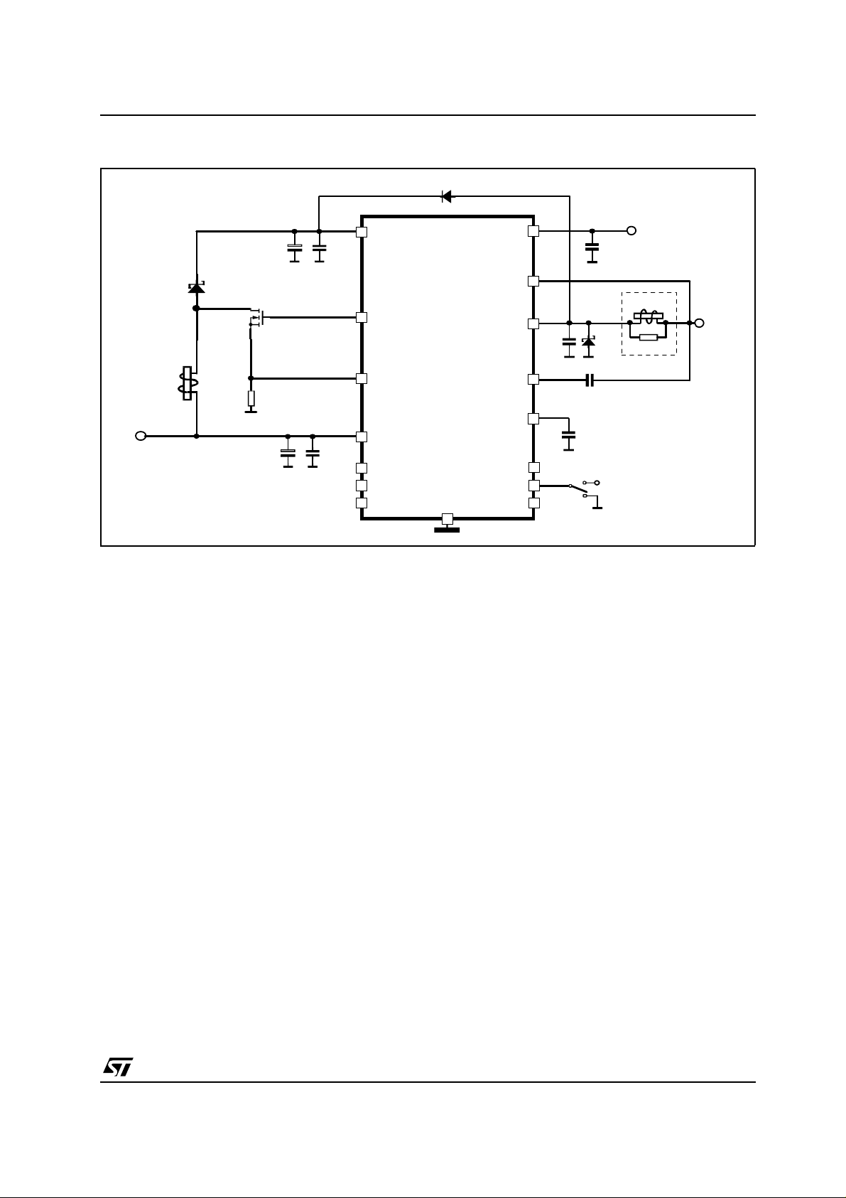
TYPICAL APPLICATION CIRCUIT
C2
220µF
Schottky
diode
STPS3L40S
or 1N5821
MOSFET
STN4NF03L
L1=22µH
Vin
12V
Rsc
0.05
ΩΩΩΩ
C1
220µF
C3
470nF
Ceramic
C4
470nF
Ceramic
IC1
DSQIN(*)
Vup
Gate
Sense
Vcc
SCL
SDA
D1 1N4001
LNBS21
GND
LT1
LT2
Vout
DETIN(*)
Byp
EXTM
ADDRESS
DSQOUT
C8
10nF
C6
10nF
C5
470nF
Master STB
C7
10nF
D2
BAT43
(**) see note
0<Vaddr<V
270µH
15 ohm
LNBS21
to LNB
Byp
(*) Set to GND if not used
(**) filter to be used according to EUTELSAT reccomendation to implement the DiSEqC
not implemented (see DiSEqC implementation note)
I2C BUS INTERFACE
Data transmission from main µP to the LNBS21
and v icev ersa takes place through the 2 wires I2C
bus interface, c ons isting of the two lines SDA and
SCL (pull-up resistors to positive supply voltage
must be externally connected).
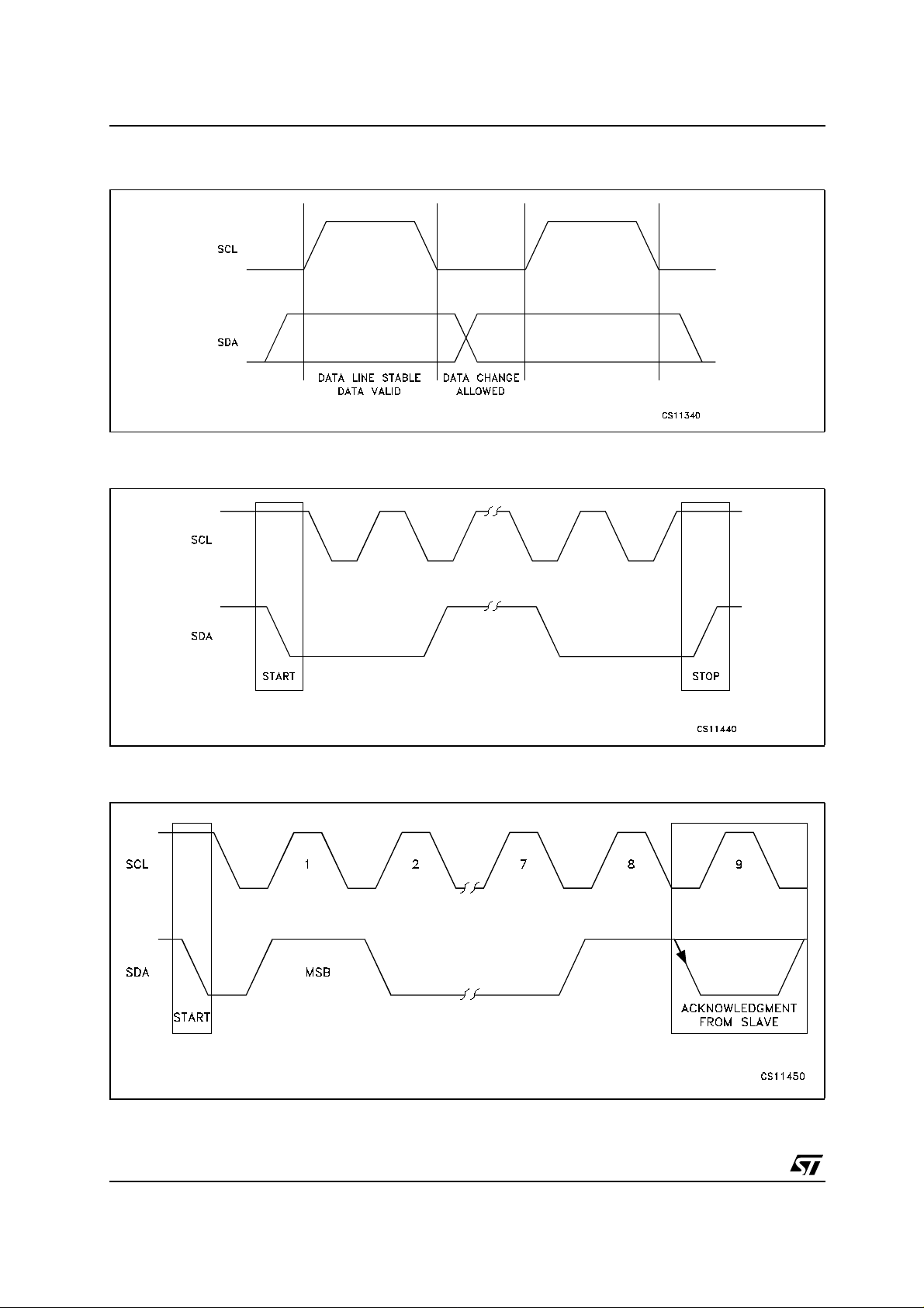
DATA VALIDITY
As shown in fig. 1, the data on t he SDA line must
be stable during the high period of the clock. The
HIGH and LOW state of the da ta line can only
change when the c lock s ignal on the SCL line is
LOW.
ACKNOWLEDGE
The master ( µP) puts a resistive HIGH l ev el on the
SDA line during the acknowledge clock pulse (see
fig. 3). The peripheral (LNBS21) that
acknowledges has to pull-down (LOW) the SDA
line during the acknowled ge clock pulse, so that
the SDA line is st able LOW during this cl ock pulse.
The peripheral which has been addressed has to
generate an ac k nowledge after the reception of
each byte, other-wise t he S D A line rema ins at the
HIGH l ev el during the ninth clock pulse time. In
this case the master transm itter can generate the
STOP information in order to abort the transfer.
START AND S TOP CONDITIONS
As shown in fig.2 a start condition is a H IG H to
LOW transition of the SDA line while SCL is HIGH.
The LNBS21 won't gen-erate the acknowledge if
the Vc c supply is below the Undervoltage Lock out
threshold (6.7V typ.).
The stop condition is a LOW t o HIGH transition of
the SDA line while SCL is HIGH. A STOP
condi-tions must be sent before each START
condition.
TRANSMISSION WITHOUT ACKNOWLEDGE
Avoiding to detect the acknowledge of the
LNBS21, th e µP can use a simpler transmission:
BYTE FORMAT
Every byte transferred to the SDA line must
contain 8 bits. Each byte must be followed by an
ac-knowledge bit. The MSB is transferred first.
simply it waits one clock without checking the
slave acknowledging, and sends the new data.
This approach of cou rse is less protected from
misworking and decreases the noise immunity.
TM
2.0,not needed if bidirectional DiSEqCTM2.0 is
5/19
LNBS21
Figure1 : DATA VALIDITY ON THE I2CBUS
2
Figure2 : TIMING DIAGRAM ON I
CBUS
Figure3 : ACKNOWLEDGE ON I
6/19
2
CBUS
 Loading...