

LCP1511D
ApplicationSpecific Discretes
A.S.D.
PROGRAMMABLE TRANSIENT VOLTAGE
SUPPRESSOR FOR SLIC PROTECTION
FEATURES
DUAL PROGRAMMABLE TRANSIENT SUPPRESSOR.
WIDENEGATIVEFIRINGVOLTAGERANGE:
=-80V max.
V
MGL
LOWDYNAMICSWITCHINGVOLTAGES:
V
FP
andV
DGL
.
LOWGATE TRIGGERINGCURRENT :
I
= 5mAmax.
GT
PEAKPULSECURRENT:
I
= 30Afor 10/1000µssurge.
PP
HOLDINGCURRENT:
I
=150mA.
H
DESCRIPTION
This device has been especially designed to protect subscriber line card interfaces (SLIC) against
transientovervoltages.
Positive overloads are clipped with 2 diodes.
Negative surges are suppressed by 2 thyristors,
theirbreakdownvoltagebeingreferenced to
throughthegate.
-V
BAT
This component presents a very low gate triggeringcurrent(I
)in ordertoreducethecurrentcon-
GT
sumption on printed circuit board during the firing
phase.
Aparticularattentionhas beengivento theinternal
wire bonding. The ”4-point” configurationensures
reliable protection, eliminating the overvoltage introducedby the parasitic inductancesof the wiring
(Ldi/dt),especiallyfor veryfast transients.
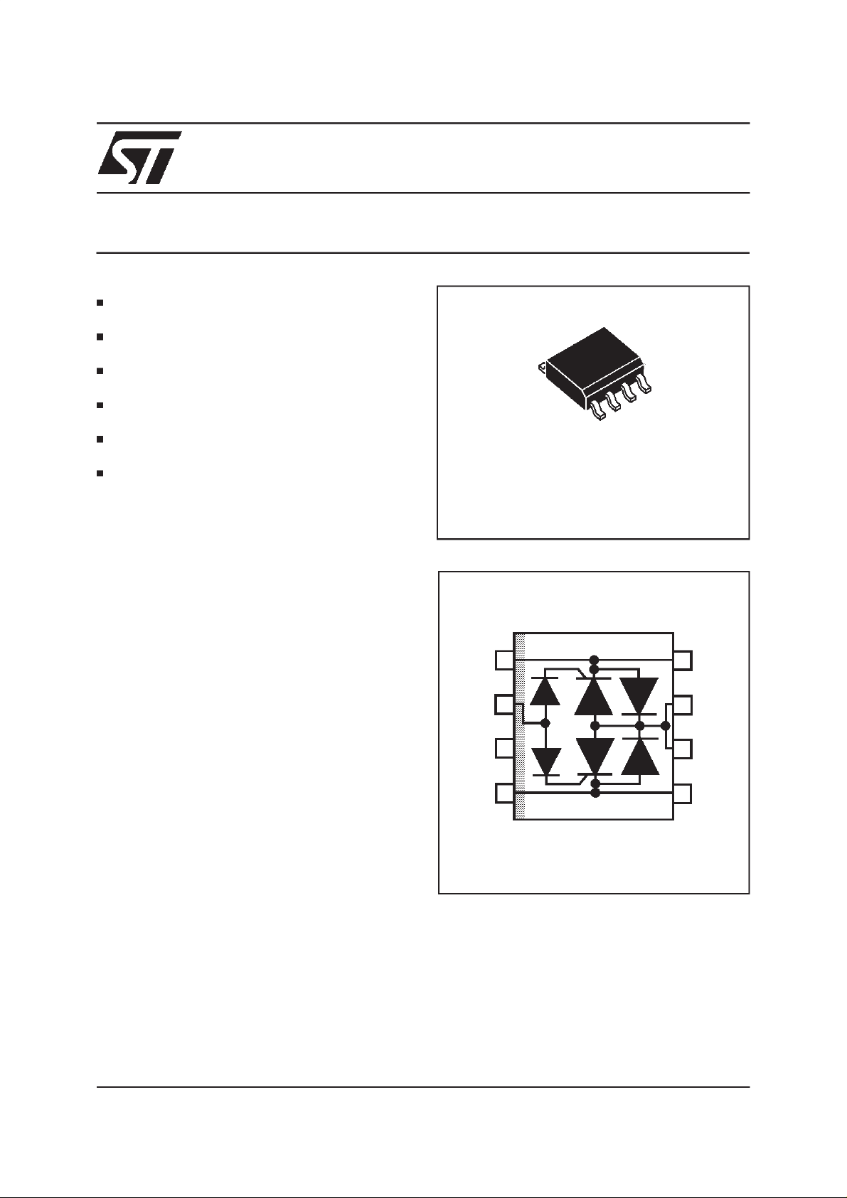
SO8
SCHEMATICDIAGRAM
TIP
1
GATE
NC
2
3
TIP
8
GND
7
GND
6
COMPLIESWITHTHEFOLLOWINGSTAN DAR DS:
CCITTK20 : 10/700µs 1kV
5/310µs 25A
VDE0433 : 10/700µs 2kV
5/310µs 38A (*)
VDE0878 : 1.2/50µs 1.5kV
1/20µs 40A
I3124 :
0.5/700µs 1kV
0.2/310µs 25A
FCCpart 68 :
2/10µs 2.5kV
2/10µs 170A (*)
BELLCORE
TR-NWT-001089: 2/10µs 2.5kV
2/10µs 170A (*)
(*)with seriesresistorsor PTC.
February 1998 Ed:3
RING
TM: ASD is trademarks ofSGS-THOMSON Microelectronics.
45
RING
1/7
LCP1511D
ABSOLUTE MAXIMUM RATINGS(T
amb
=25°C)
Symbol Parameter Value Unit
I
PP
Peakpulse current
(seenote 1)
I
TSM
Nonrepetitivesurge peak on-statecurrent
(F= 50Hz)
I
GSM
V
MLG
V
MGL
T
T
T
Note 1 : Pulse waveform :
Maximumgate current (halfsine wavetp = 10ms) 2 A
Maximumvoltage LINE / GROUND
Maximumvoltage GATE / LINE
Storagetemperaturerange
stg
Maximumjunction temperature
j
Maximumlead temperaturefor solderingduring10s 260 °C
L
10/1000µst
5/310µst
2/10µst
=10µst
r
=5µst
r
=2µst
r
=1000µs
p
=310µs
p
=10µs
p
10/1000µs
5/310µs
2/10µs
tp= 10ms
t=1s
%I
PP
100
50
30
38
170
8
3.5
-100
-80
- 55 to + 150
150
A
A
V
°C
0
t
t
r
p
t
THERMAL RESISTANCE
Symbol Parameter Value Unit
R
th (j-a)
ELECTRICALCHARACTERISTICS(T
Symbol Parameter
I
GT
I
I
RM
I
RG
V
V
V
V
V
DGL
V
GATE
V
C Off-statecapacitanceLINE/GND
Junctionto ambient 170 °C/W
=25°C)
amb
I
I
F
Gatetriggeringcurrent
Holdingcurrent
H
Reverseleakage current LINE/GND
Reverse leakage current GATE/LINE
Reversevoltage LINE/GND
RM
Forwarddrop voltageLINE/GND
F
Gatetriggeringvoltage
GT
Peakforwardvoltage LINE/GND
FP
V
GATE
V
RM
V
F
I
RM
I
H
Dynamicswitchingvoltage GATE/LINE
GATE/GNDvoltage
LINE/GNDvoltage
LG
I
PP
V
LG
2/7
LCP1511D
1 - PARAMETERSRELATEDTO THEDIODE LINE/GND(T
amb
=25°C)
Symbol Test conditions Maximum Unit
V
F
V
FP
Note 1 : See test circuit 2 for VFP;Rpis the protection resistor located on the line card.
2 - PARAMETERS RELATEDTO THE PROTECTIONTHYRISTOR
IF=5A tp=500µs3V
10/700µs 1.5kV Rp=10Ω
1.2/50µs 1.5kV R
2/10µs 2.5kV R
=10Ω (seenote 1)
p
=62Ω
p
(T
amb
=25°C)
5
7
12
Symbol Test conditions Min. Max. Unit
V
GND/LINE
V
GATE
at I
GT
Tc=25°CVRG=-75V
=70°CVRG=-75V
T
c
VGATE= -48V (seenote 3)
V
I
GT
I
V
I
RG
DGL
H
GT
10/700µs 1.5kV Rp=10Ω I
1.2/50µs 1.5kV Rp=10Ω I
2/10µs 2.5kV Rp=62Ω I
Note 2 : Seethefunctional holdingcurrent (IH) testcircuit 2.
Note 3 : Seetestcircuit 1 for V
The oscillations with a timeduration lower than50ns arenot taken into account.
=-48V 0.2 5 mA
=-48V(see note 2) 150 mA
2.5 V
5
50
10
20
25
DGL
=30A
PP
=30A
PP
=38A
PP
.
V
µA
V
3 - PARAMETERSRELATEDTO DIODEAND PROTECTIONTHYRISTOR(T
amb
=25°C)
Symbol Test conditions Maximum Unit
I
RM
C
Tc=25°CV
T
=70°CV
c
V
=-3V F=1MHz
R
=-48V F=1MHz
V
R
GATE/LINE
GATE/LINE
= -1V VRM=-75V
= -1V VRM=-75V
5
50
100
50
APPLICATIONNOTE
Inorderto take advantageofthe ”4point”structure
TIP
1
IN
OUT
8
TIP
of the LCP, the TIP and RING lines go across the
device. In such case, the devicewill eliminate the
overvoltages generated by the parasitic induc-
GATE
NC
RING
OUT
7
GND
6
5
RING
2
3
4
IN
tancesof thewiring(Ldi/dt),especiallyfor veryfast
transients.
µA
pF
3/7

LCP1511D
FUNCTIONALHOLDING CURRENT (I
) TESTCIRCUIT1 : GO-NOGO TEST
H
R
P
D.U.T.
V
=
BA T
48V
-
Surge
generator
This is a GO-NOGOtest whichallowsto confirmthe holdingcurrent (IH)level in a functionaltestcircuit.
TESTPROCEDURE:
- Adjustthecurrent levelat theI
- Firethe D.U.T. with a surgecurrent: I
- The D.U.T.will come backto theoff-statewithin a durationof 50msmax.
valuebyshort circuitingthe D.U.T.
H
= 10A,10/1000µs.
PP
TESTCIRCUIT 2 FORV
(V is defined inunload condition)
P
FP
ANDV
PARAMETERS
DGL
R
4
TIP
L
R
2
RING
R
3
V
CC
P
1
R
1
2
GND
Pulse (µs) V
t
r
t
p
p
(V) (µF) (nF) (µH) (Ω)(
10 700 1500 20 200 0 50 15 25 25 30 10
1.2 50 1500 1 33 0 76 13 25 25 30 10
2 10 2500 10 0 1.1 1.3 0 3 3 38 62
C
1
C
2
LR
1
R
2
)(
Ω
R
3
)(
Ω
R
4
Ω
IPPR
) (A) (Ω)
p
4/7

FUNCTIONAL DESCRIPTION
LINEA
LINEB
D
1
P
1
P
2
D
2
TIP
-V
BAT
C
RING
Surgepeakcurrent versus overloadduration.
I (A)TSM
10
9
8
7
6
5
4
3
2
1
0
1E-2 1E-1 1E+0 1E+1 1E+2 1E+3
t(s)
F=50Hz
Tj initial=25°C
LCP1511D
LINEA PROTECTION:
– For positive surges versus GND, the diode D1
willconduct.
– Fornegativesurges versusGND,theprotection
deviceP1will triggerat avoltagefixed by the
-V
reference.
BAT
LINEB PROTECTION:
– For surgeson line B, the operating mode is the
same,D2 or P2 is activated.
It is recommended to add a capacitor (C=220nF)
close to the gate of the LCP, in order to speedup
thetriggering.
5/7

LCP1511D
APPLICATIONCIRCUIT: typicalSLIC protection concept
RING GENERATOR
PTC
LINE A
T
E
S
LINE B
T
R
E
L
A
Y
S
THBTxxxD
PTC
RING
RELAY
LCP1511D
220
nF
-V
BAT
SLIC
ORDERCODE
LCP 15 1 1 D RL
LINE CARD
PROTECTION
I
=150mA
H
MARKING
Package Type Marking
SO8 LCP1511D CP151D
RL : tape andreel
: tube
DYNAMIC
PACKAGE
1 :SO8
VERSION
6/7

PACKAGEMECHANICAL DATA
SO8Plastic
LCP1511D
DIMENSIONS
REF.
A 1.75 0.069
a1 0.1 0.25 0.004 0.010
a2 1.65 0.065
b 0.35 0.48 0.014 0.019
b1 0.19 0.25 0.007 0.010
C 0.50 0.020
c1 45°(typ)
D 4.8 5.0 0.189 0.197
E 5.8 6.2 0.228 0.244
e 1.27 0.050
e3 3.81 0.150
F 3.8 4.0 0.15 0.157
L 0.4 1.27 0.016 0.050
M 0.6 0.024
S8°(max)
Millimetres Inches
Min. Typ. Max. Min. Typ. Max.
Weight= 0.08 g.
Packaging:Productsuppliedin antistatictubesor
tapeand reel.
Informationfurnished is believed to be accurateand reliable. However, STMicroelectronics assumes no responsibilityfor theconsequences of
use of such information nor forany infringementof patentsor other rights of thirdparties which mayresult fromitsuse. No license is granted by
implication or otherwise under any patent or patent rights of STMicroelectronics. Specifications mentioned in this publication are subject to
change without notice. This publication supersedes and replacesall information previously supplied.
STMicroelectronics products are not authorized for use as critical components in life support devices or systems without express written approval of STMicroelectronics.
1998 STMicroelectronics - Printedin Italy- All rights reserved.
STMicroelectronics GROUP OF COMPANIES
Australia- Brazil-Canada - China- France- Germany- Italy- Japan- Korea- Malaysia- Malta- Mexico - Morocco- The
Netherlands- Singapore - Spain-Sweden - Switzerland- Taiwan- Thailand- UnitedKingdom- U.S.A.
7/7
 Loading...