

LCP150S
ApplicationSpecific Discretes
A.S.D.
PROGRAMMABLE TRANSIENT VOLTAGE
SUPPRESSOR FOR SLIC PROTECTION
FEATURES
DUALPROGRAMMABLETRANSIENT
SUPPRESSOR
HIGHSURGE CURRENTCAPABILITY.
= 50A,10/1000µs.
-I
PP
= 60A,5/310 µs
-I
PP
IPP=150A,2/10µs.
-
.
HOLDINGCURRENT = 150mA min.
LOWGATE TRIGGERINGCURRENT :
=15 mA max.
I
GT
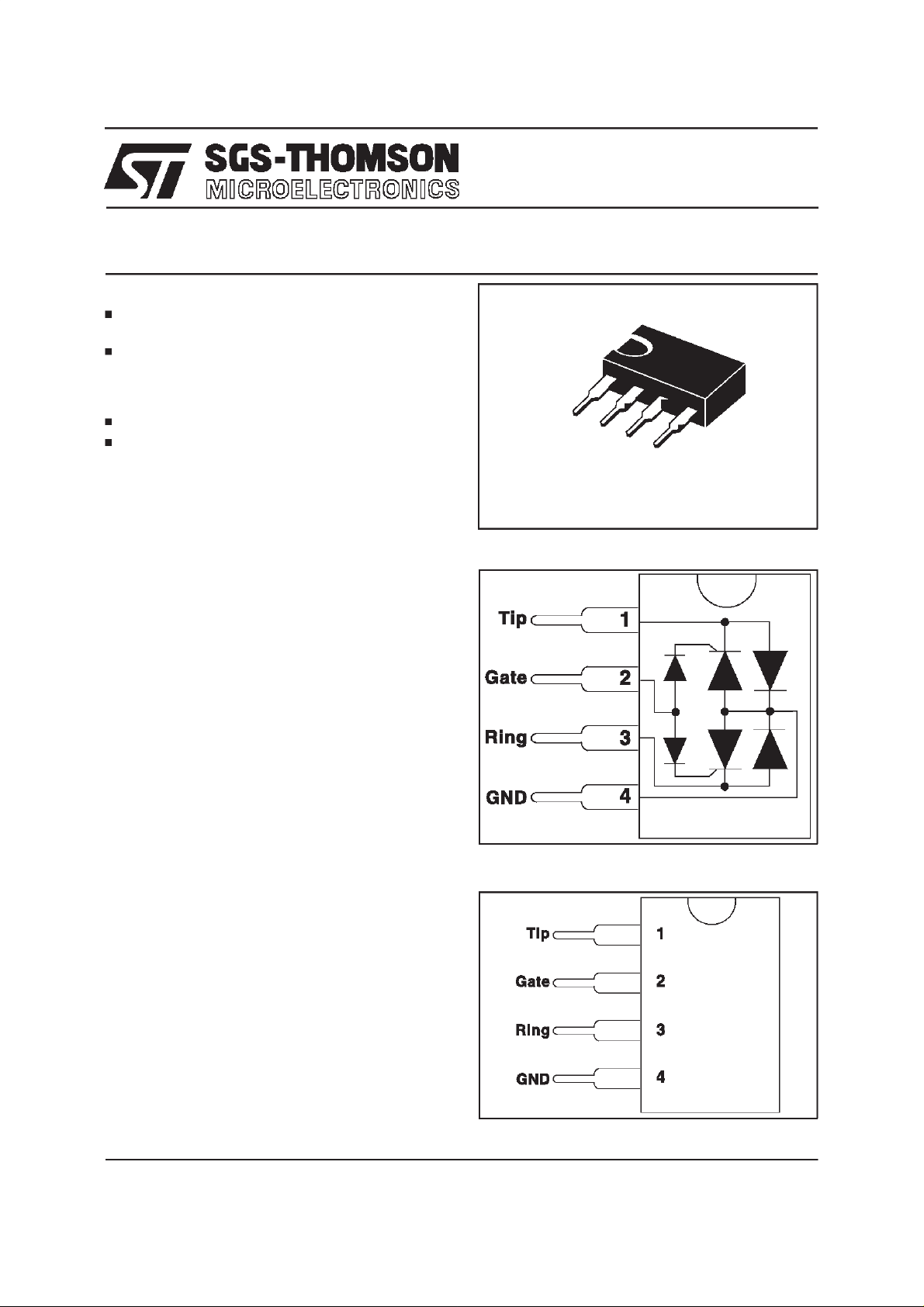
DESCRIPTION
This device has been especially designed to
protect a subscriber line card interface (SLIC)
againsttransientovervoltage.
Positive overloads are clipped with two diodes,
while negative surges are suppressed by two
protection thyristors, their breakdown voltage
beingis referencedto the -Vbat.
This component presents a very low gate
triggering current (I
) in order to reduce the
GT
current consumption on the PC board during the
firingphase.
SIP4
SCHEMATIC DIAGRAM
COMPLIES WITHTHE FOLLOWING STANDARDS:
CCITT- K20 10/700µs 1kV
5/310µs 25A
VDE0433
10/700µs 2kV
5/200µs 50A
VDE0878 1.2/50µs 1.5kV
1/20µs 40A
FCC part68
2/10µs 2.5kV
2/10µs 150A(*)
BELLCORE
TR-NWT-001089 : 2/10µs 2.5kV
2/10µs 150A(*)
10/1000µs 1kV
10/1000µs 50A(*)
CNET 0.5/700µs 1kV
0.2/310µs 25A
(*)with series resistors or PTC.
TM: ASD is trademarksof SGS-THOMSON Microelectronics.
February 1998 - Ed:3
CONNECTION DIAGRAM
1/6
LCP150S
ABSOLUTE MAXIMUMRATINGS
(T
amb
=25°C)
Symbol Parameter Value Unit
I
I
TSM
I
GSM
V
V
T
PP
MLG
MGL
stg
T
j
T
L
Peakpulsecurrent (see note 1)
Nonrepetit ivesurgepeakon-statecur re nt
F= 50 Hz
Maximumgate current(half sine wave tp = 10 ms) 2 A
MaximumVoltage LINE/GND
MaximumVoltage GATE/LINE
Storagetemperaturerange
Maximumoperatingjunctiontemperature
Maximumlead temperaturefor solderingduring 10s 260 °C
10/1000µs
5/320µs
2/10µs
tp= 10 ms
t=1s
50
60
150
25
8
- 100
-80
- 55 to + 150
150
Note 1: Pulsewaveform
10/1000µstr=10µs tp =1000µs
5/320µstr=5µs tp= 320
µs
2/10µstr=2µs, tp = 10 µs
A
A
V
C
°
C
°
%I
PP
100
50
0
t
t
r
p
t
THERMAL RESISTANCE
Symbol Parameter Value Unit
R
th (j-a)
Junction-to-ambient 80
C/W
°
2/6

ELECTRICALCHARACTERITICS (T
=25°C,unless otherwisespecified)
amb
LCP150S
Symbol Parameter
GateTrigger Current
HoldingCurrent
H
ReverseLeakageCurrent LINE/GND
R
ReverseLeakageCurrent GATE/LINE
ReverseVoltage LINE/GND
R
ForwardVoltageLINE/GND
F
GateTrigger Voltage
GT
PeakForward Voltage LINE/GND
FP
DynamicSwitchingVoltage
V
I
I
V
V
V
GT
I
I
RG
V
SGL
VSGL VR
I
F
I
VF
IR
IH
GND/LINE
V
gate
V
C
GATE/GNDVoltage
LINE/GNDVoltage
LG
OffState CapacitanceLINE/GND
Ipp
1 - PARAMETERS RELATED TO THE DIODE LINE/GND
Symbol Test Conditions Max. Unit
V
V
Squarepulse,Tp = 500µs, IF=5A 3 V
F
Ipp= 40 A, 10/1000µs. 15 V
FP
VGL
2 - PARAMETERSRELATED TO PROTECTION THYRISTOR
Symbol TestsConditions Min. Max. Unit
V
I
V
I
GT
I
H
GT
RG
SGL
V
GND/LINE
V
GATE
atI
Tc= 25°CV
Tc= 70°CV
V
GATE
= -48 V 0.2 15 mA
= -48 V Note 2 150 mA
GT
RG
RG
= -75V
= -75V
2.5 V
5
50
= -48 V Note 2 - 63 V
µ
µA
3 - PARAMETERSRELATIVE TODIODE AND PROTECTIONTHYRISTOR
Symbol TestsConditions Min. Max. Unit
I
R
Tc= 25°C-1<V
Tc= 70°C-1<V
CV
Note 2 : See test circuit for IHand V
= - 3 V F < 1MHz
R
= - 48 V F < 1MHz
V
R
SGL
< -Vbat VR= - 85 V
GL
< -Vbat VR= - 85 V
GL
5
50
150
80
.
µ
µ
pF
pF
A
A
A
3/6

LCP150S
Fig. 1 : Surge peak current versus overload
duration(typicalvalues).
I (A)
TSM
30
25
20
15
10
5
0
1E-2 1E-1 1E+0 1E+1 1E+2 1E+3
t(s)
FUNCTIONAL HOLDING CURRENT (IH) TEST CIRCUIT = GO - NOGO TEST.
Tj initial = 25°C
R
Vbat = - 48V
SGL
V
Ipp = 10A,10/1000 s
Thisis a GO-NOGOTest which allowsto confirm the holdingcurrent (IH) levelin a functional
testcircuit.
Thistest can be performedif thereferencetest circuitcan’t be implemented.
TESTPROCEDURE:
1) Adjustthe currentlevel at the IH value by short circuitingthe AK of the D.U.T.
2) Firethe D.U.T with a surgeCurrent : Ipp = 10A, 10/1000µs.
3) TheD.U.T will come backto theOFF-Statewithin a durationof 50 msmax.
TheV
is measuredjustbeforefiring
SGL
-Vpp
4/6

APPLICATIONCIRCUIT
TypicalSLIC ProtectionConcept.
RING
GENERATOR
-V
LCP150S
BAT
LINE A
LINE B
T
E
S
T
R
E
L
A
Y
S
PTC
PTC
FUNCTIONAL DESCRIPTION
THBT200S
RING
RELAY
220
nF
LCP150S
LINEA PROTECTION:
- For positivesurgesversus GND,the diodeD1
will conduct.
- For negativesurgesversus GND, the protection deviceP1 will trigger at a voltagefixed by
the -VBATreference.
SLIC
LINEB PROTECTION:
- For surgeson LineB, the operatingmode is the
same, D2 or P2 is activated.
A capacitor(C = 220nF)can be addedclose to
the gateof theLCP15xx,in orderto speedup
the triggering.
5/6

LCP150S
MARKING : Logo,Date Code, LCP150S.
ORDERCODE
LCP 150 S
LINE CARD PROTECTION
HOLDING CURRENT : 150 mA
PACKAGEMECHANICAL DATA
SIP4
PACKAGE
S = SIP4PLASTIC
DIMENSIONS
REF.
Millimetres Inches
Min. Typ. Max. Min. Typ. Max.
A 7.10 0.280
a1 2.80 0.110
B 10.15 0.400
b1 0.50 0.020
b2 1.35 1.75 0.053 0.069
c1 0.38 0.50 0.015 0.020
e 2.54 0.100
e3 7.62 0.200
I 10.50 0.413
L 3.30 0.130
Z 1.50 0.059
PACKAGING
WEIGHT
Information furnished is believed to be accurate and reliable. However, SGS-THOMSON Microelectronics assumes no responsibility for the
consequences of use of such information nor for any infringement of patents or other rights of thirdparties which may result from its use. No
license is grantedby implication or otherwise under any patentor patent rights of SGS-THOMSON Microelectronics.Specifications mentioned
in this publication are subject to change withoutnotice.This publication supersedes and replacesall informationpreviously supplied.
SGS-THOMSONMicroelectronics productsare notauthorizedforuse as criticalcomponentsin lifesupport devices or systems withoutexpress
written approval of SGS-THOMSON Microelectronics.
Australia- Brazil - Canada - China - France - Germany - Italy - Japan - Korea - Malaysia - Malta - Morocco
The Netherlands - Singapore - Spain -Sweden - Switzerland - Taiwan - Thailand - United Kingdom -U.S.A.
6/6
:Productssuppliedinantistatictubes.
: 0.55g
1998 SGS-THOMSON Microelectronics - Printed in Italy - All rights reserved.
SGS-THOMSON MicroelectronicsGROUP OF COMPANIES
 Loading...