

L2 96
HIGHCURRENT SWITCHING REGULATORS
4 A OUTPUT CURRENT
.
5.1 V TO40 V OUTPUTVOLTAGERANGE
.
0 TO 100 % DUTY CYCLERANGE
.
PRECISE(±2 %)ON-CHIP REFERENCE
.
SWITCHINGFREQUENCY UP TO 200KHz
.
VERYHIGH EFFICIENCY(UP TO90 %)
.
VERYFEW EXTERNALCOMPONENTS
.
SOFTSTART
.
RESETOUTPUT
.
EXTERNALPROGRAMMABLELIMITING
.
CURRENT(L296P)
CONTROLCIRCUIT FORCROWBAR SCR
.
INPUTFORREMOTEINHIBITAND
.
SYNCHRONUSPWM
THERMALSHUTDOWN
.
DESCRIP TION
TheL296andL296Parestepdownpowerswitching
regulatorsdelivering4 A at a voltagevariable from
5.1V to 40V.
Featuresof thedevicesincludesoftstart,remotein-
hibit, thermal protection, a reset output for microprocessors and a PWM comparatorinput for synchronizationin multichipconfigurations.
TheL296Pincudesexternalprogrammablelimiting
current.
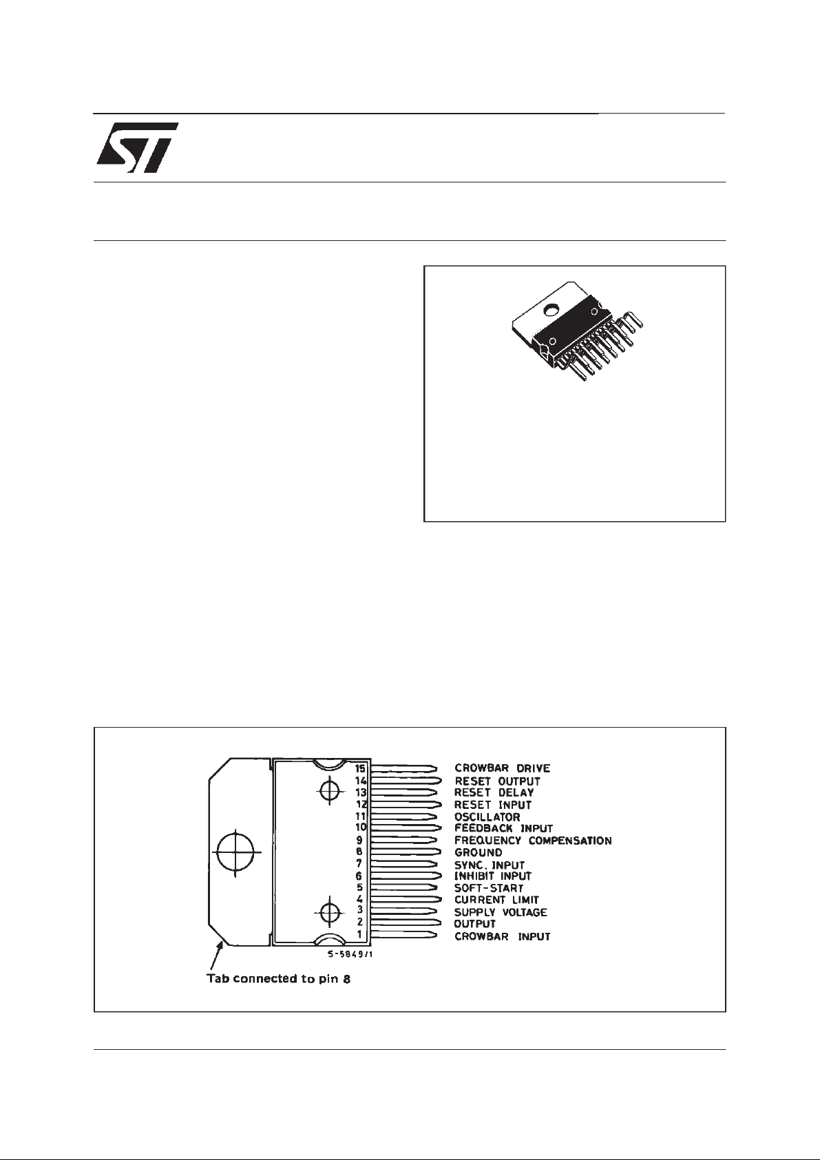
L296P
Multiwatt
(15 lead)
ORDERING NUMBERS :
L296 (Vert ic a l) L296HT (Hor i z ontal)
L296P (Ver t ic al) L296PH T (Horizontal)
TheL296andL296Paremountedina 15-leadMultiwattplasticpowerpackageandrequiresveryfew
externalcomponents.
Efficient operation at switching frequencies up to
200 KHz allows a reductionin the size and costof
external filter components. A voltage sense input
and SCR drive output are provided for optional
crowbar overvoltage protection with an external
SCR.
PIN C ONNE CTION (top view)
June 2000
1/22
L296 - L296P
PIN FUNCTIONS
N
°
1 CROWBAR INPUT Voltage Sense Input for Crowbar Overvoltage Protection. Normally connected to the
2 OUTPUT Regulator Output
3 SUPPLY VOLTAGE Unrergulated Voltage Input. An internal Regulator Powers the L296s Internal Logic.
4 CURRENT LIMIT A resistor connected between this terminal and ground sets the current limiter
5 SOFT START Soft Start Time Constant. A capacitor is connected between this terminal and ground
6 INHIBIT INPUT TTL – Level Remote Inhibit. A logic high level on this input disables the device.
7 SYNC INPUT Multiple L296s are synchronized by connecting the pin 7 inputs together and omitting
8 GROUND Common Ground Terminal
9 FREQUENCY
10 FEEDBACK INPUT The Feedback Terminal on the Regulation Loop. The output is connected directly to
11 OSCILLATOR A parallel RC networki connected to this terminal determines the switching frequency.
12 RESET INPUT Input of the Reset Circuit. The threshold is roughly 5 V. It may be connected to the
13 RESET DELAY A capacitor connected between this terminal and ground determines the reset signal
14 RESET OUTPUT Open collector reset signal output. This output is high when the supply is safe.
15 CROWBAR OUTPUT SCR gate drive output of the crowbar circuit.
Name Function
feedback input thus triggering the SCR when V
also monitor the input and a voltage divider can be added to increase the threshold.
Connected to ground when SCR not used.
threshold. If this terminal is left unconnected the threshold is internally set (see
electrical characteristics).
to define the soft start time constant. This capacitor also determines the average
short circuit output current.
the oscillator RC network on all but one device.
COMPENSATION
A series RC network connected between this terminal and ground determines the
regulation loop gain characteristics.
this terminal for 5.1V operation ; it is connected via a divider for higher voltages.
This pin must be connected to pin 7 input when the internal oscillator is used.
feedback point or via a divider to the input.
delay time.
exceeds nominal by 20 %. May
out
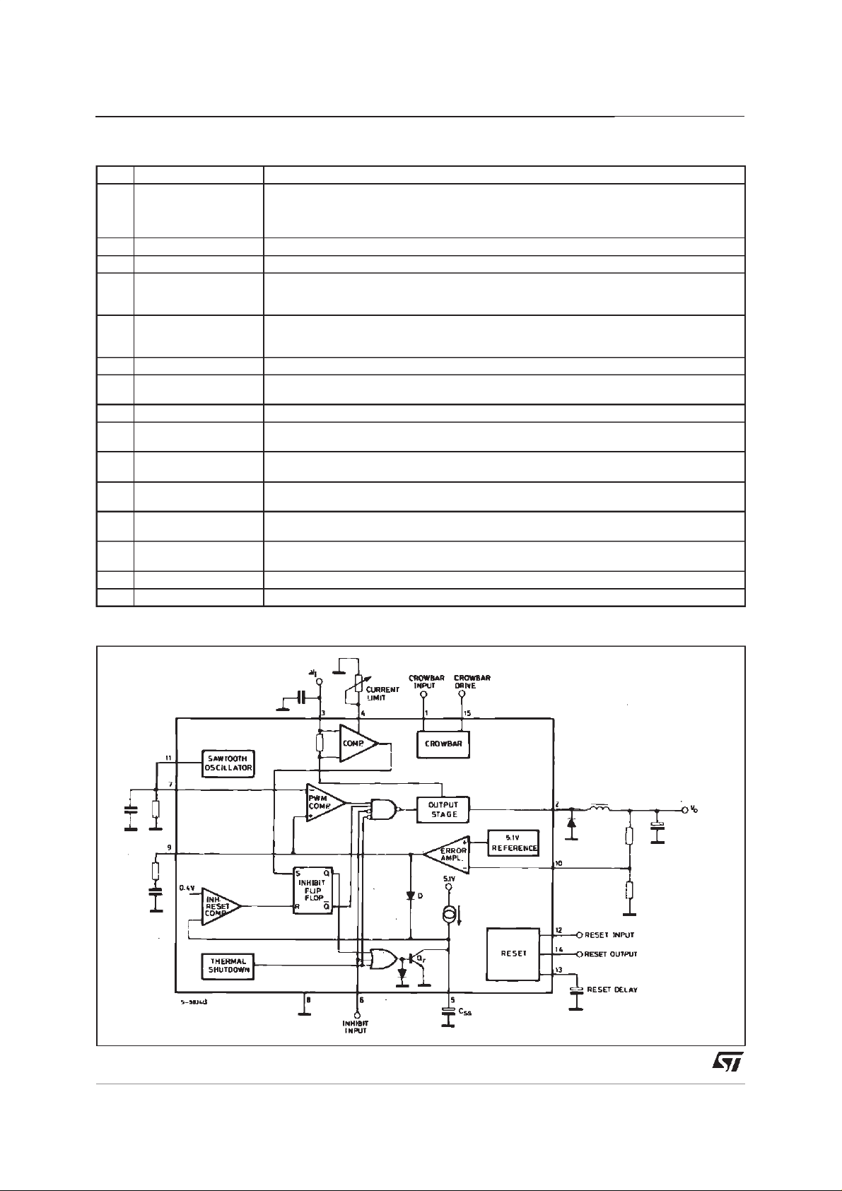
BLOCK DIAGRAM
2/22
L296 - L296P
CIRCUIT OPERATION
(refer to the block diagram)
The L296 and L296P are monolithic stepdown
switchingregulatorsprovidingoutputvoltagesfrom
5.1Vto 40Vand delivering 4A.
Theregulationloopconsistsofasawtoothoscillator,
erroramplifier,comparatorandtheoutputstage.An
error signal is produced by comparing the output
voltagewithaprecise5.1Von-chipreference(zener
zaptrimmedto ±2%).Thiserrorsignalisthencomparedwiththe sawtoothsignalto generatethefixed
frequencypulsewidthmodulatedpulseswhichdrive
theoutputstage.The gainandfrequencystabilityof
theloopcanbeadjustedby anexternalRCnetwork
connectedtopin9.Closingtheloopdirectlygivesan
outputvoltageof5.1V.Highervoltagesareobtained
by insertinga voltagedivider.
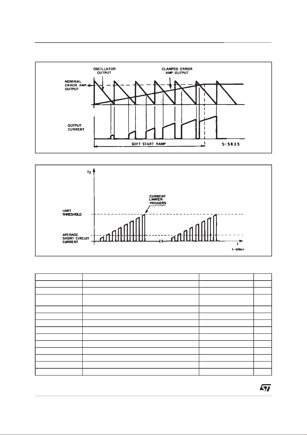
Outputovercurrentsat switch on areprevented by
the soft start function. The error amplifier output is
initially clamped by the externalcapacitorCss and
allowedto rise,linearly,as thiscapacitorischarged
by a constantcurrent source.
Outputoverloadprotectionisprovidedintheformof
a current limiter. The load current is sensed by an
internalmetal resistor connected to a comparator.
Whenthe load current exceedsa presetthreshold
this comparator sets a flip flop which disables the
outputstageanddischargesthesoftstartcapacitor.
A second comparator resetsthe flip flop when the
voltageacross the soft start capacitorhas fallen to
0.4V. The output stage is thus re-enabled and the
output voltage rises under control of the soft start
network.If the overloadconditionisstill presentthe
limiterwill trigger againwhen the thresholdcurrent
is reached.The averageshort circuitcurrent islimitedto a safevalue bythe deadtime introducedby
the softstart network.
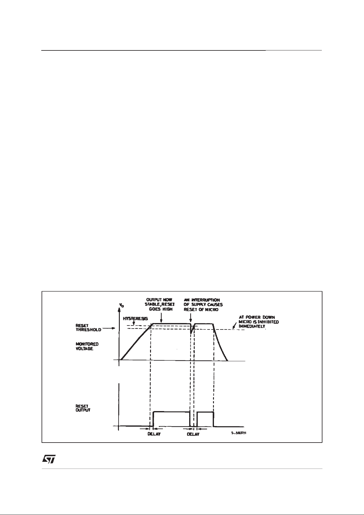
The reset circuit generates an output signal when
the supply voltage exceeds a threshold programmed byan externaldivider.Thereset signalis
generatedwitha delaytimeprogrammedby an external capacitor. When the supply falls below the
threshold the reset output goes low immediately.
The resetoutput isan opencollector.
Thescrowbarcircuitsensestheoutputvoltage and
the crowbar outputcan providea currentof 100mA
toswitchonan externalSCR.ThisSCRistriggered
when the output voltage exceeds the nominal by
20%. There is no internal connectionbetween the
outputand crowbarsenseinputthereforethe crowbarcan monitoreitherthe inputor theoutput.
ATTL- levelinhibitinputis providedforapplications
suchasremoteon/offcontrol.Thisinputis activated
byhighlogiclevelanddisablescircuitoperation.After an inhibitthe L296 restartsunder controlof the
softstart network.
The thermaloverloadcircuit disablescircuitoperation when the junction temperature reaches about
150°Candhas hysteresistopreventunstableconditions.
Figure 1 :Reset OutputWaveforms
3/22
L296 - L296P
Figure 2 :Soft StartWaveforms
Figure 3 :CurrentLimiter Waveforms
ABSOLUTE MAXIMUM RATINGS
Symbol Parameter Value Unit
V
i
V
i–V2
V
2
V
1,V12
V
15
,V5,V7,V9,V13Voltage at Pins 4, 5, 7, 9 and 13 5.5 V
V
4
,V
V
10
6
V
14
I
9
I
11
I
14
P
tot
,T
T
j
stg
4/22
Input Voltage (pin 3) 50 V
Input to Output Voltage Difference 50 V
Output DC Voltage
Output Peak Voltage at t = 0.1µsec f = 200KHz
–1
–7
Voltage at Pins 1, 12 10 V
Voltage at Pin 15 15 V
Voltage at Pins 10 and 6 7 V
Voltage at Pin 14 (I14≤ 1 mA) V
i
Pin 9 Sink Current 1 mA
Pin 11 Source Current 20 mA
Pin 14 Sink Current (V14< 5 V) 50 mA
Power Dissipation at T
case
C20W
≤90°
Junction and Storage Temperature – 40 to 150
V
V
C
°
L296 - L296P
THERMAL DATA
Symbol Parameter Value Unit
R
th j-case
R
th j-amb
ELECTRICAL CHARACTERISTICS
(refer to the test circuits T
Symbol Parameter Test Conditions Min. Typ. Max. Unit Fig.
DYNAMIC CHARACTERISTICS (pin 6 to GND unless otherwise specified)
V
o
V
i
V
i
∆V
o
V
∆
o
V
ref
∆ V
ref
T
∆
V
d
I
2L
I
SH
η Efficiency I
SVR Supply Voltage Ripple Rejection
f Switching Frequency 85 100 115 kHz 4
f
∆
V
∆
i
∆ f
T
∆
j
f
max
T
sd
DC CHARACTERISTICS
I
3Q
–I
2L
Thermal Resistance Junction-case Max. 3 °C/W
Thermal Resistance Junction-ambient Max. 35
=25oC, Vi= 35V, unless otherwise specified)
j
Output Voltage Range Vi= 46V, Io=1A V
Input Voltage Range Vo=V
to 36V, I
ref
Input Voltage Range Note (1), Vo=V
Line Regulation Vi=10V to 40V, Vo=V
Load Regulation Vo=V
ref
Io=2Ato4A
= 0.5A to 4A
I
o
3A 9 46 V 4
≤
o
to 36V Io=4A 46 V 4
REF
=2A 15 50 mV 4
ref,Io
ref
40 V 4
101530
45
C/W
°
mV 4
Internal Reference Voltage (pin 10) Vi= 9V to 46V, Io= 2A 5 5.1 5.2 V 4
Average Temperature Coefficient
of Reference Voltage
Dropout Voltage Between Pin 2
and Pin 3
Current Limiting Threshold (pin 2) L296 - Pin 4 Open,
T
=0°C to 125°C, Io= 2A 0.4 mV/°C
j
2
Io=4A
=2A
I
o
1.3
3.2
2.1
4.5 7.5 A 4
= 9V to 40V, Vo=V
V
i
L296P - V
= 9V to 40V, Vo=V
i
Pin 4 Open
= 22k
R
Iim
Ω
ref
to 36V
ref
5
2.5
7
4.5
V
V
A4
Input Average Current Vi= 46V, Output Short-circuited 60 100 mA 4
Voltage Stability of Switching
=3A
o
V
o=Vref
Vo= 12V
=2V
V
∆
i
V
o=Vref,Io
rms,fripple
=2A
= 100Hz
75
85
50 56 dB 4
Vi= 9V to 46V 0.5 % 4
%4
Frequency
Temperature Stability of Switching
Tj=0°C to 125°C1%4
Frequency
Maximum Operating Switching
Frequency
Thermal Shutdown Junction
Vo=V
= 1A 200 kHz –
ref,Io
Note (2) 135 145
C–
°
Temperature
Quiescent Drain Current Vi= 46V, V7= 0V, S1 : B, S2 : B
=0V
V
6
=3V
V
6
Output Leakage Current Vi= 46V, V6= 3V, S1 : B, S2 : A,
=0V
V
7
66
30
85
40
2mA
4
4
mA
Note (1): Using min.7 Aschottky diode.
(2):Guaranteed by design, not 100 % tested in production.
5/22
L296 - L296P
ELECTRICAL CHARACTERISTICS
(continued)
Symbol Parameter Test Conditions Min. Typ. Max. Unit Fig.
SOFT START
I
I
Source Current V6= 0V, V5= 3V 80 130 150
5so
Sink Current V6= 3V, V5= 3V 50 70 120
5si
A6b
µ
A6b
µ
INHIBIT
V
V
–I
–I
Input Voltage
6L
6H
Input Current
with Input Voltage
6L
6H
Low Level
High Level
Low Level
High Level
= 9V to 46V, V7= 0V,
V
i
S1 : B, S2 : B – 0.3
2
= 9V to 46V, V7= 0V,
V
i
S1 : B, S2 : B
= 0.8V
V
6
=2V
V
6
0.8
5.5
10
3
V6a
A6a
µ
ERROR AMPLIFIER
V
V
I
–I
High Level Output Voltage V10= 4.7V, I9= 100µA,
9H
Low Level Output Voltage V10= 5.3V, I9= 100µA,
9L
Sink Output Current V10= 5.3V, S1 : A, S2 : B 100 150
9si
Source Output Current V10= 4.7V, S1 : A, S2 : D 100 150 µA6c
9so
Input Bias Current V10= 5.2V, S1 : B
I
10
DC Open Loop Gain V9= 1V to 3V, S1 : A, S2 : C 46 55 dB 6c
G
v
S1 : A, S2 : A
S1 : A, S2 : E
= 6.4V, S1 : B, L296P
V
10
3.5 V 6c
0.5 V 6c
2
2
10
10
A6c
µ
AµA6c
µ
OSCILLATOR AND PWM COMPARATOR
–I
–I
Input Bias Current of
7
PWM Comparator
Oscillator Source Current V11= 2V, S1 : A, S2 : B 5 mA
11
V7= 0.5V to 3.5V 5
A6a
µ
RESET
V
12 R
V
12 F
V
13 D
V
13 H
V
14 S
I
–I
I
13 si
I
Rising Threshold Voltage
= 9V to 46V,
V
i
Falling Threshold Voltage 4.75 V
S1 : B, S2 : B
Delay Thershold Voltage
V
= 5.3V, S1 : A, S2 : B
Delay Threshold Voltage
12
V
ref
-150mV
4.3 4.5 4.7 V 6d
V
ref
-100mV
ref
-150mV
100 mV 6d
Hysteresis
Output Saturation Voltage I14= 16mA, V12= 4.7V, S1, S2 : B 0.4 V 6d
Input Bias Current V12=0VtoV
12
= 3V, S1 : A, S2 : B
V
Delay Source Current
13 so
Delay Sink Current
Output Leakage Current Vi= 46V, V12= 5.3V, S1 : B, S2 : A 100 µA6d
14
13
V
12
V
12
, S1 : B, S2 : B 1 3
ref
= 5.3V
= 4.7V
70
10
110 140
V
ref
-50mV
V
ref
-100mV
V6d
V6d
A6d
µ
A
µ
mA
CROWBAR
V
Input Threshold Voltage S1 : B 5.5 6 6.4 V 6b
1
V
–I
Output Saturation Voltage Vi= 9V to 46V, Vi= 5.4V,
15
I
Input Bias Current V1= 6V, S1 : B 10
1
Output Source Current Vi= 9V to 46V, V1= 6.5V,
15
= 5mA, S1 : A
I
15
= 2V, S1 : B
V
15
70 100 mA 6b
0.2 0.4 V 6b
A6b
µ
6c
6d
6/22
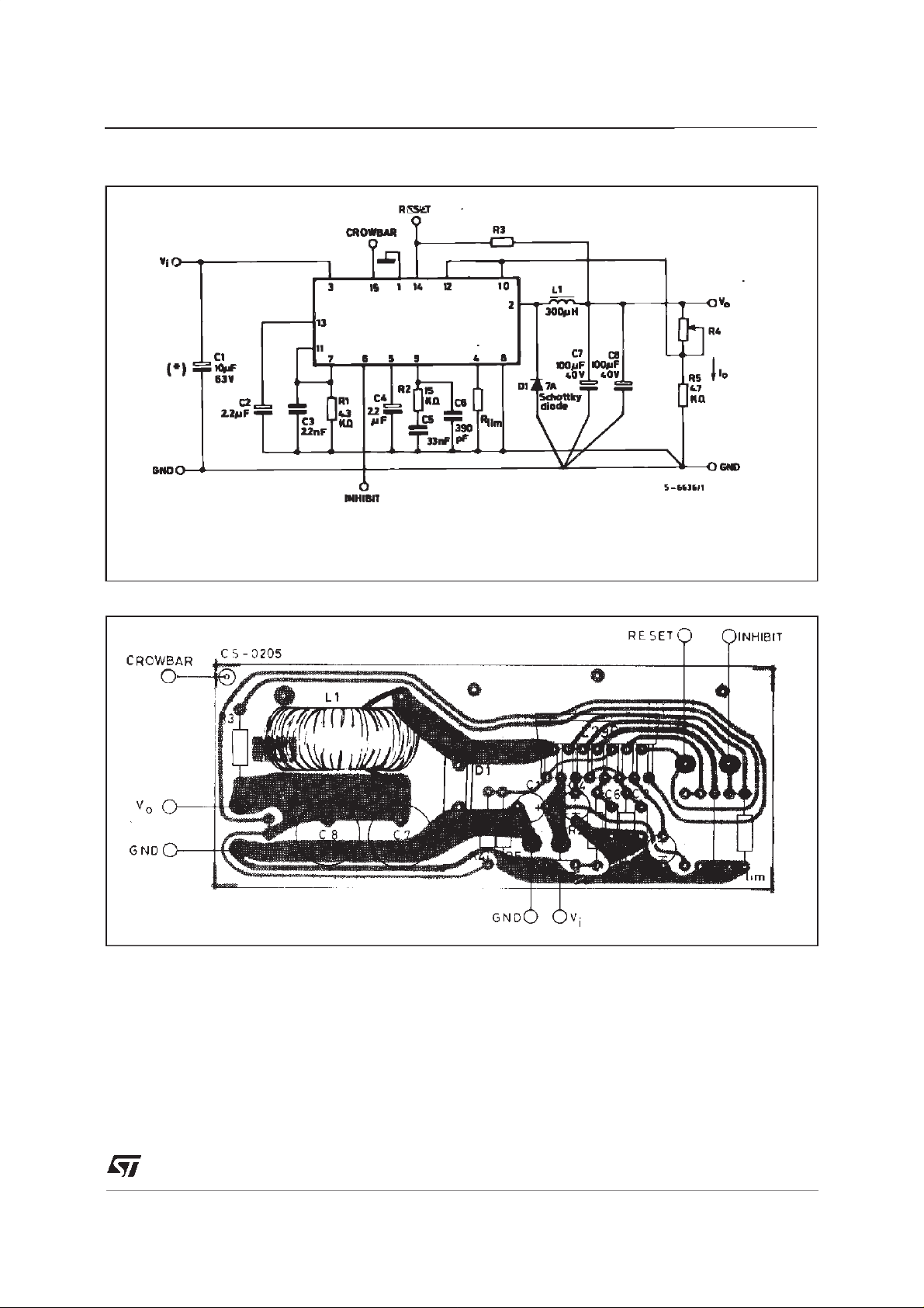
Figure4 : DynamicTest Circuit
C7, C8 : EKR (ROE)
L1 : L = 300µH at8 A Core type : MAGNETICS 58930 - A2 MPP
N°turns: 43 Wire Gauge : 1mm (18 AWG) COGEMA946044
(*)Minimum suggested value (10 µF) to avoid oscillations.Rippleconsideration leads to typicalvalue of 1000 µF or higher.
L296 - L296P
Figure 5 : PC. Boardand ComponentLayoutof the Circuitof Figure4 (1:1scale)
7/22
 Loading...