

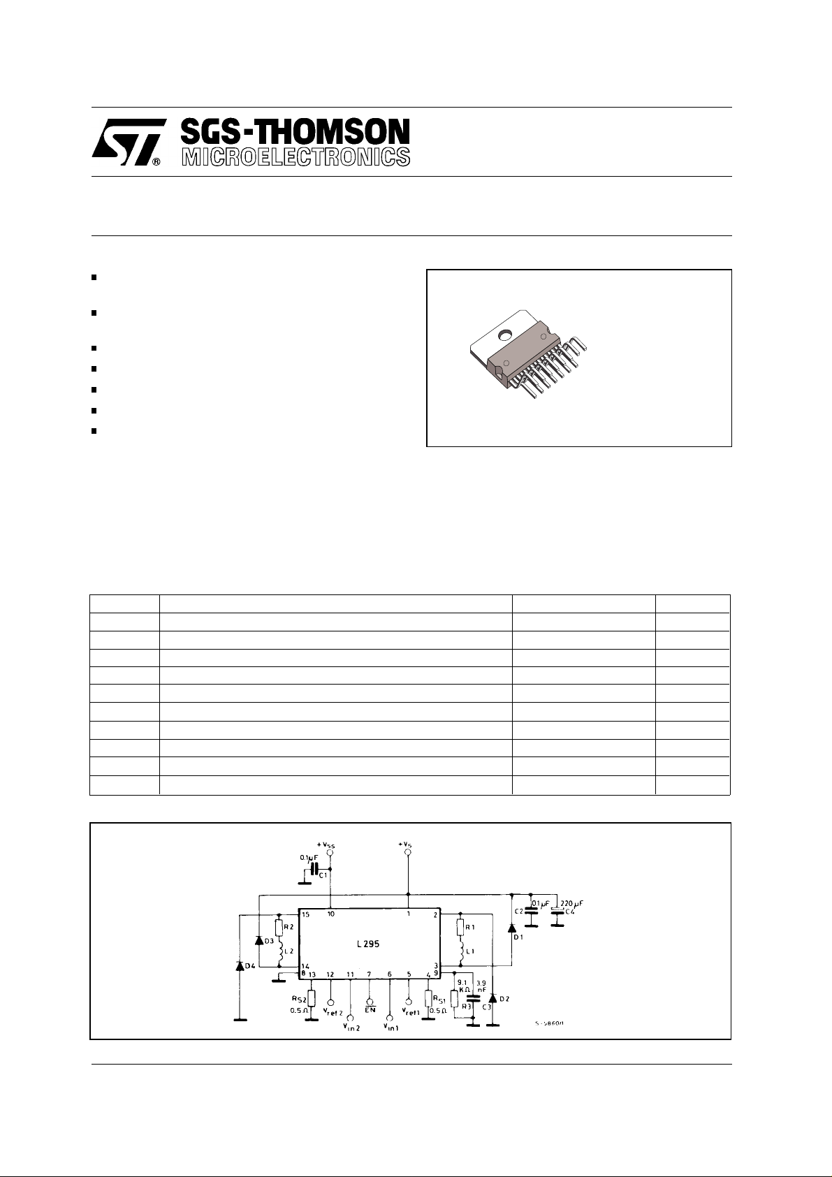
DUAL SWITCH-MODE SOLENOID DRIVER
PRELIMINARY DATA
HIGH CURRENT CAPABILITY (up to 2.5A per
channel)
HIGH VOLTAGE OPERATION (up to 46V for
power stage)
HIGH EFFICIENCY SWITCHMODE OPERATION
REGULATED OUTPUT CURRE NT (adjus table)
FEW EXTERNAL COMPONENTS
SEPARATE LOGIC SUPPLY
THERMAL PROTECTION
ORDER CODE : L295
DESCRIPTION
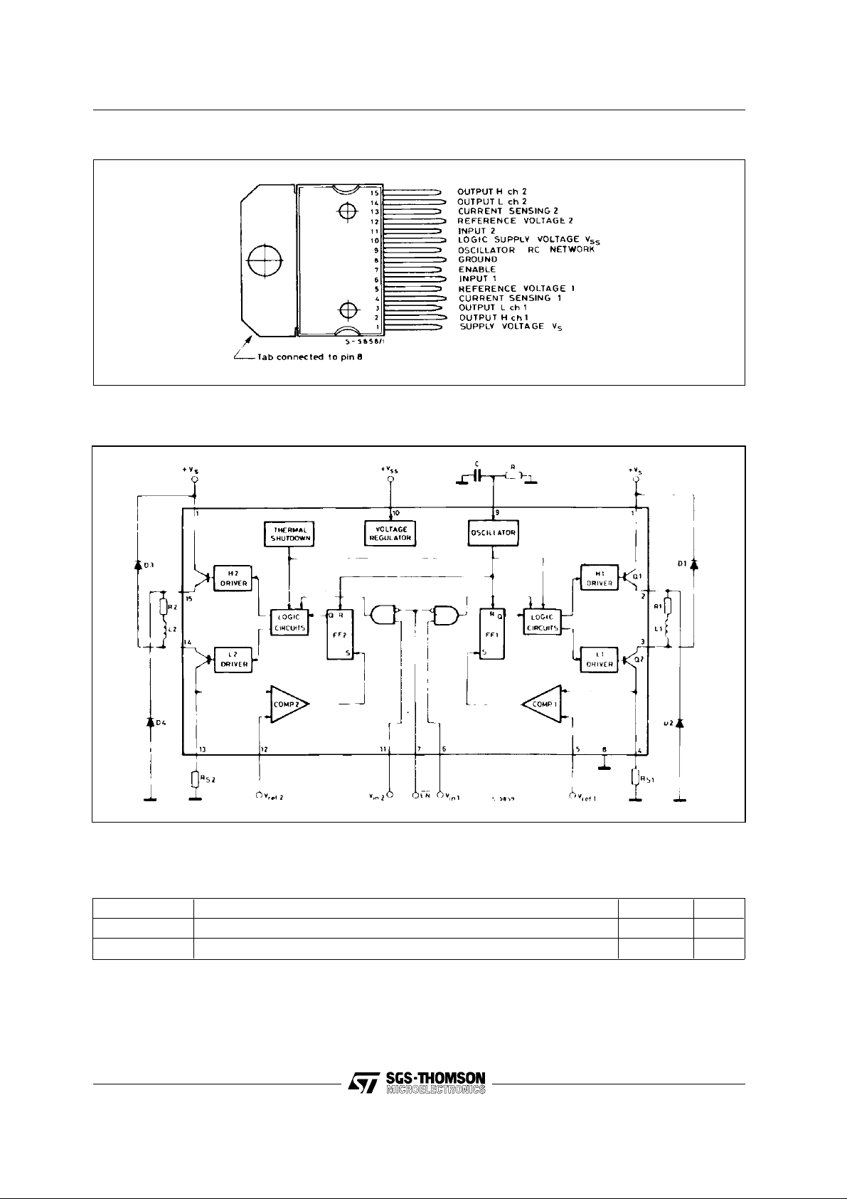
The L295 is a monolithic integrated circuit in a 15 lead Multiwatt ® package; it incorporates all the
functions for direct interfacing between digital circuitry and inductive loads. The L295 is designed to
accept standard micr oproces sor logic levels at th e
inputs and can drive 2 solenoids. The output curr ent
is completely controlled by means of a switch-
ing technique allowing very efficient operation.
Furthermore, it includes an enable input and dual
supplies (for interfac ing with peripherals r unning at
a higher voltage than the logic).
The L295 is particularly suitable for applications
such as hammer driving in matrix printers, step
motor driving and electromagnet controllers.
ABSOLUT E MAX IMUM R ATINGS
Symbol Parameter Value Unit
V
s
V
ss
V
, V
EN
V
ref
Io Peak output current (each channel)
Ptot
Tstg, Tj Storage and junction temperature - 40 to 150
Supply voltage 50 V
Logic supply voltage 12 V
Enable and input voltage 7 V
i
Reference voltage 7 V
- non repetitive (t = 100 µsec)
- repetitive (80% on - 20% off; Ton = 10 ms) 2.5 A
- DC operation 2 A
Total power dissipation (at Tcase = 75 °C
3A
25 W
Multiwatt 15
L295
°C
APPLIC ATION CIRCUIT
March 1993
1/8
L295
CONNECT IO N DIAG R AM (top view)
BLOCK DIAGRAM
THERMAL DATA
Symbol Parameter Value Unit
2/8
R
th-j-case
R
th-j-amb
Thermal resistance junction-case max 3
Thermal resistance junction-ambient max 35
°C/W
°C/W

L295
ELECTRICAL CHARACTERISTICS (Refer to the application circuit, Vss = 5V, Vs = 36V; Tj = 25°C; L =
Low; H = High; unless otherwise specified)
Symbol Parameter Test conditions Min. Typ. Max. Unit
V
Supply Voltage 12 46 V
s
Logic Supply Voltage 4.75 10 V
V
ss
I
Quiescent drain current
d
(from VSS)
VS = 46V; Vi1 = Vi2 = VEN = L
4mA
IssQuiescent drain current
(from VS)
V
,,Vi2Input Voltage Low -0.3 0.8
i1
VSS = 10 V
High 2.2 7
V
Enable Input Voltage Low -0.3 0.8
EN
High 2.2 7
, Ii2Input Current Vi1 = Vi2 = L -100
I
i1
V
I
Enable Input Current VEN = L -100
EN
V
,
V
I
V
I
ref2
F
Input Reference Voltage
ref1
ref2
,
Input Reference Voltage
ref1
m
Oscillation Frequency C = 3.9 nF;
osc
I
p
Transconductance (each ch.) V
V
ref
= 1V 1.9 2 2.1 A/V
ref
= Vi2 = H 10
i1
= H 10
EN
0.2 2 V
R = 9.1 KΩ
25 KHz
46 mA
V
V
µA
µA
-5
µA
(*) V
V
V
V
Total output voltage drop
drop
(each channel) (*)
External sensing resistors
sens1
voltage drop
sens2
drop
= V
CEsat Q1
+ V
CEsat Q2.
Io = 2 A
2.8 3.6 V
2V
3/8
 Loading...