

SWITCH-MODE SOLENOID DRIVER
HIGH VOL TAGE OPERATION (UP TO 50V)
HIGH OUTPUT CURRENT CAP ABILITY (UP TO 4A)
LOW SA TURATION VOLTAGE
TTL-COM PATIBLE INPUT
OUTPUT SHORT CIRCUIT PROTECTI ON (TO
GROUND, TO SUPPLY AND ACROSS THE
LOAD)
THERMAL SHU TDOWN
OVERDRIVING PROTECTION
LATCHED DIAGNO S TIC OU TP UT
DESCRIPTION
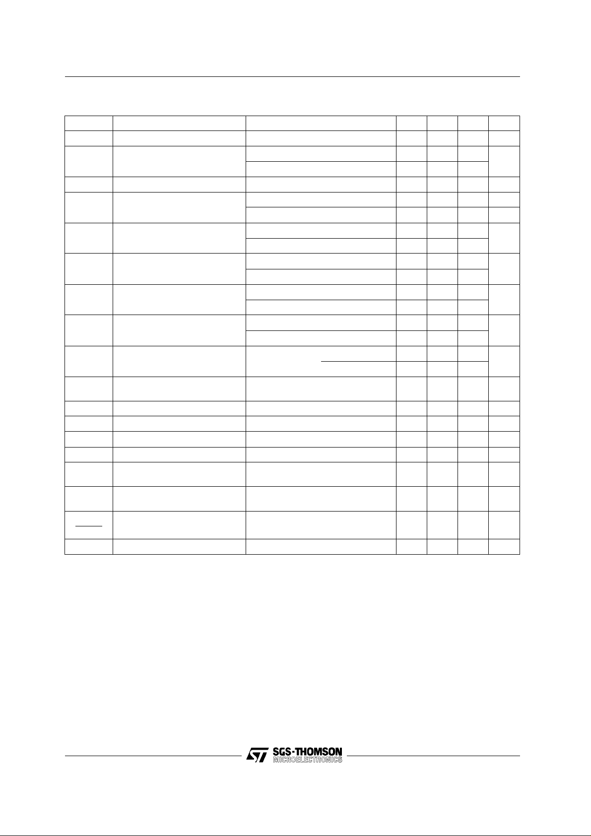
The L294 is a monolithic switched mode solenoid
driver designed for fast, high current applications
such as hummer and needle driving in printers and
electronic typewriters. Power dissipation is reduced by efficient s wit c hm od e o pe ra ti on . A n e xtra
L294
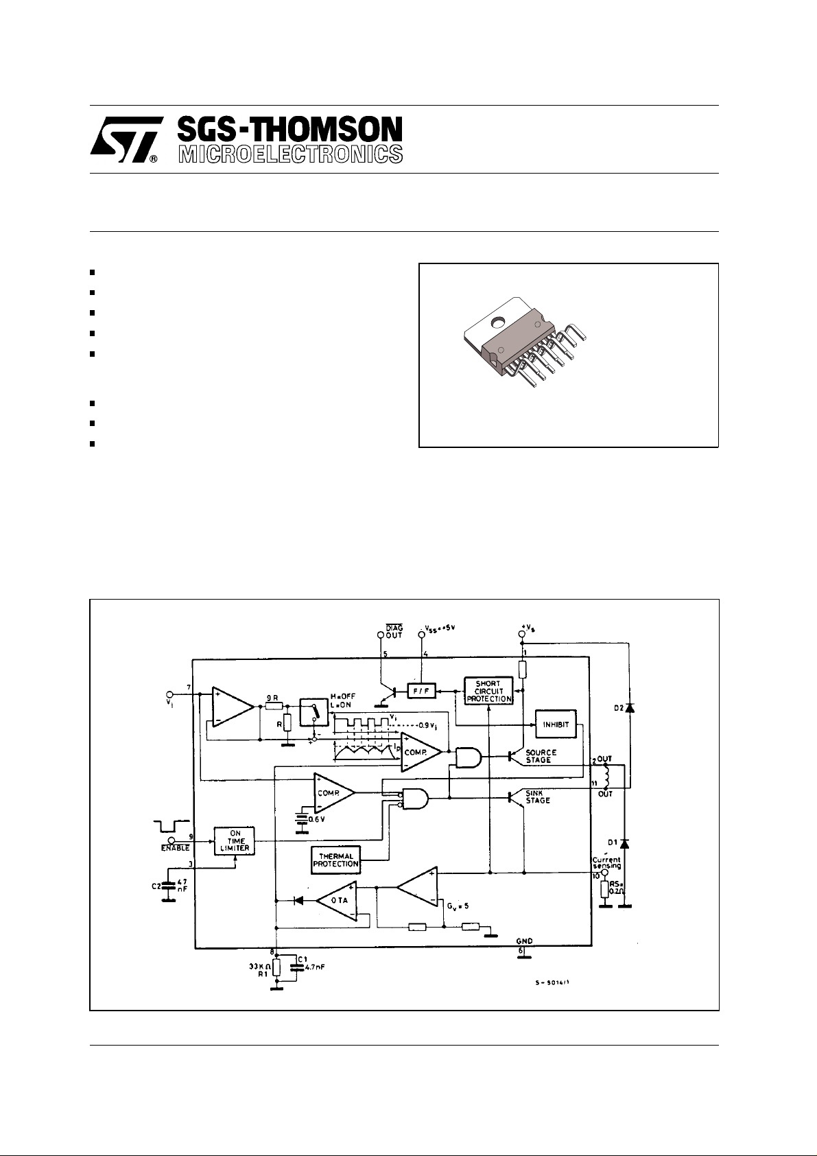
Multiwatt 11
ORDER CODE : L294
feature of the L294 is a latched diagnostic output
which indicates when the output is short circuited.
The L294 is supplied in a 1 1-lead Multiw att® plastic power package.
BLOCK DIAGR A M
October 1991
1/8

L294
ABSOLUTE MAXIMUM RATING
Symbol Parameter Value Unit
V
s
V
SS
V
EN
I
p
P
tot
T
, T
stg
Power Supply Voltage 50 V
Logic Supply Voltage 7 V
Enable Voltage 7 V
Peak Output Current (repetitive) 4.5 A
Total Power Dissipation (at T
Storage and Junction Temperature - 40 to 150
j
CONNECT IO N DIAG RA M (top view)
= 75 °C)
case
25 W
°C
THERMAL DATA
Symbol Parameter Value Unit
Rth-j-case Thermal resistance junction-case Max 3
2/8
°C/W
L294
ELECTRICAL CHARACTERISTICS (refer to the test circuit, Vs = 40 V, Vss = 5V, T
= 25 °C, unless
amb
otherwise specified)
Symbol Parameter Test conditions Min. Typ. Max. Unit
V
I
V
I
ss
V
I
V
ENABLE
I
ENABLE
I
load
V
sat H
V
sat L
V
sat H + VsatL
I
leakage
K On Time Limiter Constant (°) V
V
DIAG
I
DIAG
V
pin
V
pin
V
SENS
(°) After a time interval t
(°°) See the block diagram.
(°°°) Allowed range of V
Power Supply Voltage (pin 1) Operative Condition 12 46 V
s
Quiescent Drain Current (pin 1) V
d
Logic Suply Voltage (pin 4) 4.5 7 V
ss
Quiescent Logic Supply
Current
Input Voltage (pin 7) Operating Output 0.6 V
i
= H 20 30
ENABLE
Vi ≥ 0.6V; V
V
= L 5 8 mA
DIAG
ENABLE
= L
70
DIAG Output at High Impedance 10 100
Non-operative Output 0.45
Input Current (pin 7)
i
≥ 0.6V
V
i
V
≤ 0.45V
i
-3
-1
Enable Input Voltage (pin 9) Low Level -0.3 0.8
High Level 2.4
Enable Input Current (pin 9) V
/ ViTrasconductance
Source Output Saturation
= L -100
ENABLE
= H 100
V
ENABLE
V
= 0.2 Ω
R
S
= 1V 0.95 1 1.05
i
V
= 4V 0.97 1 1.3
i
Ip = 4A 1.7 V
Voltage
Sink Output Saturation Voltage Ip = 4A 2 V
Total Saturation Voltage Ip = 4A 4.5 V
Output Leakage Current
Diagnostic Output Voltage
Rs = 0.2Ω; Vi ≤ 0.45 V
= L 120
ENABLE
I
= 10 mA 0.4 V
DIAG
(pin 5)
Diagnostic Leakage Current
V
= 40V 10
DIAG
(pin 5)
8
OP AMP and OTA CD V oltage
Gain (°°)
10
V
= 100 to 800 mV 5
pin 10
Sensing Voltage (pin 10) (°°°) 0.9 V
= KC2, the output stages are disabled.
max
without intervention of the short circuit p rotect ion.
SENS
1mA
mA
µA
µA
V
µA
A/V
µA
3/8
 Loading...