

PUSH-PULL FOURCHANNEL DRIVERS
.OUTPUT CURRENT 1APER CHANNEL
.PEAK OUTPUTCURRENT 2A PER CHANNEL
(nonrepetitive)
.INHIBITFACILITY
.HIGHNOISE IMMUNITY
.SEPARATELOGICSUPPLY
.OVERTEMPERATURE PROTECTION
L293B
L293E
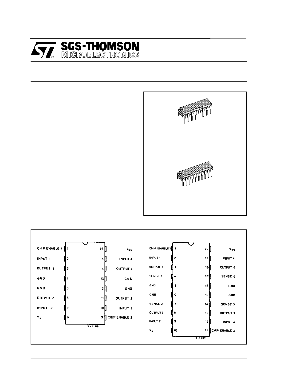
DIP16
DESCRIPTION
The L293Band L293E are quad push-pulldrivers
capableofdeliveringoutputcurrentsto1Aperchannel.Eachchanneliscontrolledbya TTL-compatible
logicinput andeach pair of drivers(a fullbridge) is
equippedwith an inhibitinput whichturnsoffallfour
transistors.A separatesupply input is provided for
the logicso that itmay be run offa lowervoltageto
reducedissipation.
Additionally,the L293E has externalconnectionof
sensingresistors, for switchmode control.
TheL293BandL293Earepackagein16and20-pin
plasticDIPs respectively; both use the four center
pinsto conductheat to the printedcircuitboard.
PIN CONNECTIONS
DIP16 - L293B POWERDIP (16+2+2) - L293E
ORDERING NUMBER : L293B
POWERDIP (16 + 2+ 2)
ORDERING NUMBER : L293E
April1993
1/12
L293B - L293E
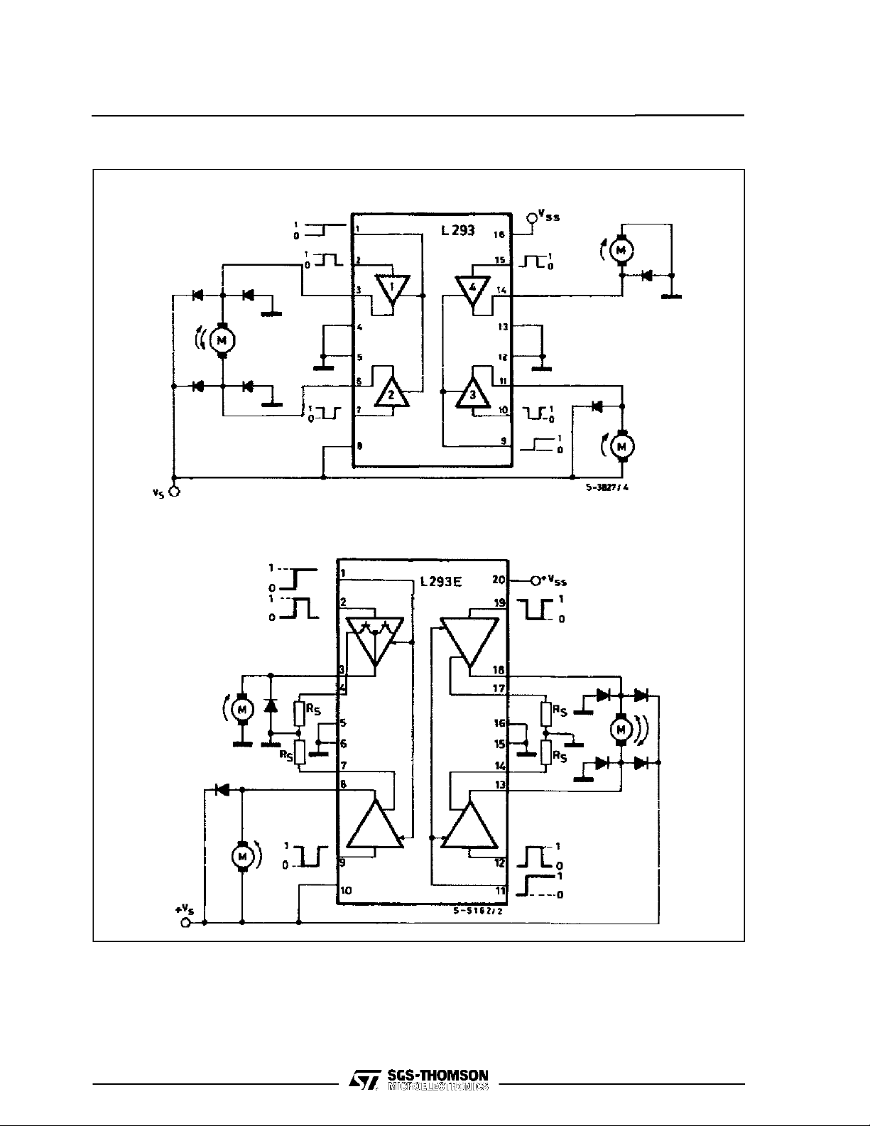
BLOCK DIAGRAMS
DIP16 - L293B
POWERDIP (16+2+2) - L293E
2/12
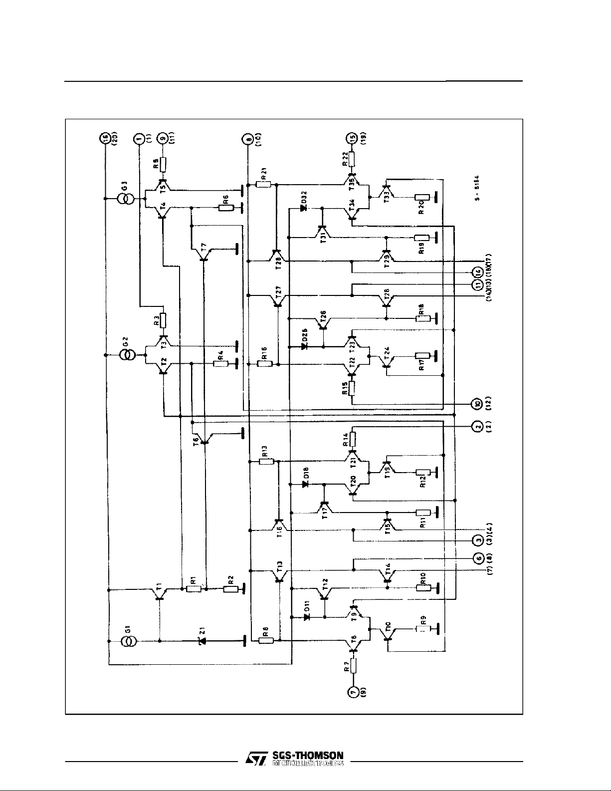
SCHEMATIC DIAGRAM
L293B - L293E
(*) In the L293 these points are not externally available. They are internally connected to the ground (substrate).
O Pins of L293 () Pins of L293E.
3/12
L293B - L293E
ABSOLUTE MAXIMUM RATINGS
Symbol Parameter Value Unit
V
V
V
I
P
T
stg,Tj
THERMAL DATA
Symbol Parameter Value Unit
R
th j-case
R
th j-amb
ELECTRICAL CHARACTERISTICS
For each channel, V
Symbol Parameter Test Conditions Min. TYp. Max. Unit
V
V
I
V
V
I
V
V
I
inhL
I
inhH
V
CEsatH
V
CEsatL
V
SENS
t
t
* See figure 1
** Referred to L293E
Supply Voltage 36 V
s
Logic Supply Voltage 36 V
ss
V
Input Voltage 7 V
i
Inhibit Voltage 7 V
inh
Peak Output Current (non repetitive t = 5ms) 2 A
out
Total Power Dissipation at T
tot
ground-pins
=80oC5W
Storage and Junction Temperature –40 to +150
Thermal Resistance Junction-case Max. 14
Thermal Resistance Junction-ambient Max. 80
= 24V, VSS= 5V, T
S
Supply Voltage V
s
Logic Supply Voltage 4.5 36 V
ss
I
Total Quiescent Supply Current Vi=L Io=0 V
s
Total Quiescent Logic Supply Current Vi=L Io=0 V
ss
Input Low Voltage -03. 1.5 V
iL
Input High Voltage VSS≤ 7V
iH
I
Low Voltage Input Current Vil= 1.5V -10 µA
iL
High Voltage Input Current 2.3V ≤ VIH≤ Vss- 0.6V 30 100 µA
iH
Inhibit Low Voltage -0.3 1.5 V
inhL
Inhibit High Voltage VSS≤ 7V
inhH
Low Voltage Inhibit Current V
High Voltage Inhibit Current 2.3V ≤ V
=25oC, unless otherwise specified
amb
=H
=H Io=0 V
V
i
=H Io=0 V
V
i
>7V
V
ss
>7V
V
ss
= 1.5V -30 -100 µA
inhL
≤ Vss- 0.6V ±10 µA
inhH
V
V
inh
inh
inh
inh
inh
inh
=H
=L
=H
=H
=L
ss
2
16
44
16
16
2.3
2.3
2.3
2.3
Source Output Saturation Voltage Io= -1A 1.4 1.8 V
Sink Output Saturation Voltage Io= 1A 1.2 1.8 V
Sensing Voltage (pins 4, 7, 14, 17) (**) 2 V
t
Rise Time 0.1 to 0.9 Vo(*) 250 ns
r
t
Fall Time 0.9 to 0.1 Vo(*) 250 ns
f
Turn-on Delay 0.5 Vito 0.5 Vo(*) 750 ns
on
Turn-off Delay 0.5 Vito 0.5 Vo(*) 200 ns
off
o
o
36 V
6
24
4
60
22
24
V
ss
7
V
ss
7
o
C
C/W
C/W
mA
mA
V
V
TRUTH TABLE
Vi(each channel) V
H
L
H
L
(*) High output impedance
(**) Relative to the considerate channel
4/12
H
X(
X(
(∞)
o
V
inh
H
L
o
)
o
)
H
L
L
 Loading...