

SGS Thomson Microelectronics HCF4538M013TR, HCF4538BM1, HCF4538BEY Datasheet
HCF4538B
DUAL MONOSTABLE MULTIVIBRATOR
■ RETRIGGERABLE/RESETTABLE
CAPABILITY
■ TRIGGER AND RESET PROPAGATION
DELAYS INDEPENDENT OF R
■ TRIGGERING FROM LEADING OR
, C
X
X
TRAILING EDGE
■ Q AND Q BUFFERED OUTPUT AVAILABLE
■ SEPARATE RESETS
■ WIDE RANGE OF OUTPUT PULSE WIDTHS
■
QUIESCENT CURRENT SPECIFIED UP TO
20V
■ 5V, 10V AND 15V PARAMETRIC RATINGS
■ SCHMITT TRIGGER INPUT ALLOWS
UNLIMITED RISE AND FALL TIMES ON +TR
AND -TR INPUTS
■ INPUT LEAKAGE CURRENT
I
= 100nA (MAX) AT VDD = 18V TA = 25°C
I
■ 100% TESTED FOR QUIESCENT CURRENT
■ MEETS ALL REQUIREMENTS OF JEDEC
JESD13B " STANDARD SPECIFICAT IONS
FOR DESCRIPTI ON OF B SERI ES CMOS
DEVICES"
DESCRIPTION
The HCF4538B is a m onolithic integrated circuit
fabricated in Metal Oxide Semiconductor
technology available in DIP and SOP packages.
The HCF4538B dual precision monostable
multivibrator provides stable retriggerable/
resettable one-shot operation for any fixed voltage
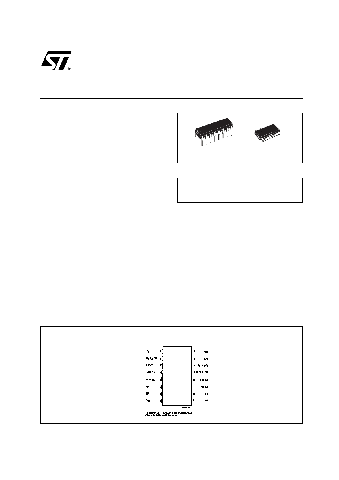
DIP SOP
ORDER CODES
PACKAGE TUBE T & R
DIP HCF4538BEY
SOP HCF4538BM1 HCF4538M013TR
timing application. An external resistor (R
an external capacitor (C
) control the timing and
X
accuracy for the circuit. Adjustment of R
) and
X
and C
X
provides a wide range of output pulse widths from
the Q and Q
terminals. The time delay from trigger
input to output transition (trigger propagation
delay) and the time delay from reset input to
output transition (reset propagation delay) and the
time delay from reset input to output transition
(reset propagation delay) are ind ependent of R
and CX. Precision control of output pulse width is
achieved through linear CMOS techniques.
Leading edge triggering (+TR) and trailing edge
triggering (-TR) inputs are pro vided for triggering
X
X
PIN CONNECTION
1/10September 2001
HCF4538B
from either edge of an input pulse. An unused +TR
input should be tied to V
should be tied to V
DD
. An unused -TR input
SS
. A RESET (o n lo w leve l) is
provided for immediate termination of the output
pulse or to prevent output pulses when power is
turned on. An unused RESET input should be tied
to V
. However, if an entire section of the
DD
HCF4538B is not used, its inputs must be tied to
either V
or VSS (see table 1). In normal
DD
operation the circuit triggers (ext ends the output
pulse one period) on the ap plication of each new
trigger pulse. For operation in the non-retiggerable
mode, Q
is connected to -TR when leading edge
triggering (+TR) is used or Q is connected to +TR
when trailing edge triggering (-TR) is used. The
time period (T) for this multivibrator can be
calculated by : T = R
external resistance, R
min. values of externa l capacitance, C
µF and 5n F, respectively.
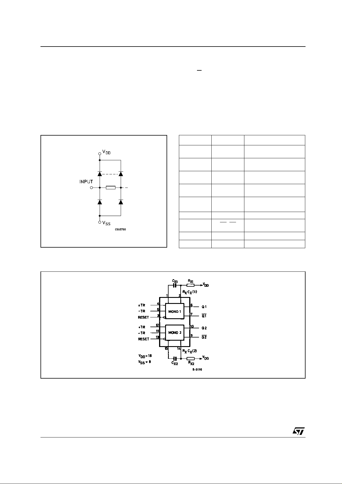
IINPUT EQUIVALENT CIRCUIT PIN DESCRIPTION
PIN No SYMBOL NAME AND FUNCTION
4, 12 +TR
5, 11 -TR
3, 13 RE SET
1, CX2
1, 15
2, 14
6, 10 Q1, Q2 Pulse Outputs
7, 9 Q1
8
16
Terminals 1, 8, 15 are el ectrically connected i nternally
C
X
R
XCX
R
XCX
, Q2
V
SS
V
DD
. The min. value of
X CX
, is 4KΩ. The max. and
X
Trigger Inputs (Low to
High, Edge-Triggered)
Trigger Inputs (High to
Low, Edge-Triggered)
Direct Reset Inputs
(Active Low)
External Capacitor Connections
1
External Resistor/Capaci-
2
tor Connections
Complementary Pulse
Outputs
Negative Supply Voltage
Positive Supply Voltage
, are 100
X
FUNCTIONAL DIAGRAM
2/10
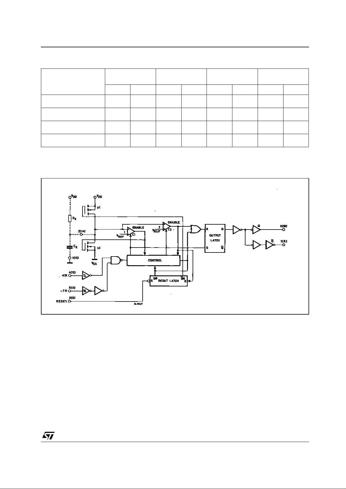
TABLE 1 : Func ti onal Termi nal Co nnections
HCF4538B
Input Pulse to
Term. N°
Other Connections
FUNCTION
to Term. N° VSS to Term. N°
V
DD
Mono (1) Mono (2) Mono (1) Mono (2) Mono (1) Mono (2) Mono (1) Mono (2)
Leading Edge Trigger/
Retriggerable
Leading Edge Trigger/Non
Retriggerable
Trailing Edge Trigger/
Retriggerable
Trailing Edge Trigger/Non
Retriggerable
A Retriggerable one-shot multivibrator has an output pulse width which is extended on full time period (T) after application of the last trigger
pulse .
A Non-Retriggerable one-s hot multiv ibrator has a time period (T ) referenced from th e application of the fir s t ri gger pulse .
3, 5 11, 13 4 12
3 13 4 12 5, 7 11, 9
3 13 4 12 5 11
3 13 5 11 4, 6 12, 10
LOGIC DIAGRAM
3/10
 Loading...