


.CASCADABLE IN MULTIPLES OF 4-BITS
.SET TO9 INPUTAND 9 DETECT OUTPUT
.QUIESCENT CURRENT SPECIFIED TO 20V
FOR HCC DEVICE
.STANDARDIZED SYMMETRICAL OUTPUT
CHARACTERISTICS
.5V, 10VAND 15V PARAMETRIC RATINGS
.INPUT CURRENTOF 100nA AT 18V AND25
FOR HCC DEVICE
o
.100% TESTEDFOR QUIESCENTCURRENT
.MEETSALLREQUIREMENTSOFJEDECTEN-
TATIVE STANDARD N. 13A, ” STANDARD
SPECIFICATIONS FOR DESCRIPTION OF B
SERIESCMOS DEVICES ”
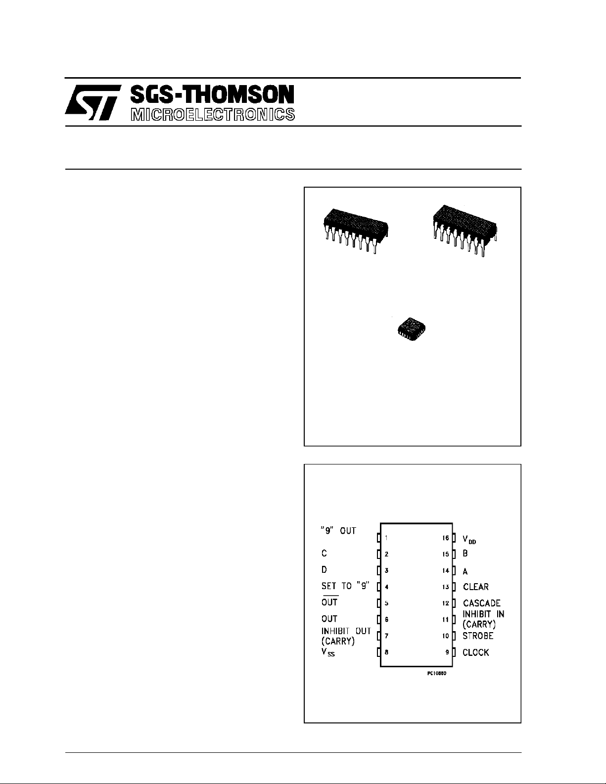
HCC4527B
HCF4527B
BCD RATE MULTIPLEXER
C
EY
(PlasticPackage)
F
(CeramicPackage)
C1
(ChipCarrier)
DESCRIPTION
TheHCC4527B (extended temperature range) and
HCF4527B (intermediate temperature range) are
monolithic integrated circuit, available in 16-lead
dual in line plastic or ceramicpackage.
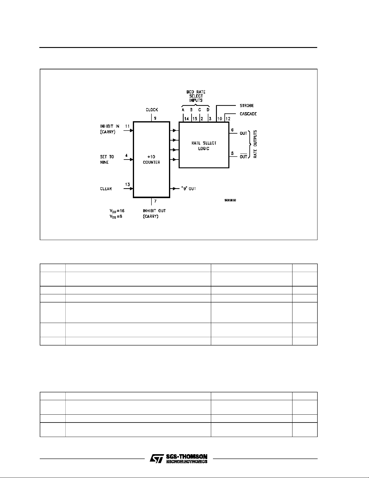
TheHCC/HCF4527Bisalow power4bitdigital rate
multiplier thatprovidesan output pulserate whichis
theclockinputpulseratemultipliedby1/10timesthe
BCD input. For example, when the BCDinput is 8,
there will be 8 output pulses for every 10 input
pulses. This device may be used to preform arithmetic operations (add, subtract, divide, raise to a
power), solve algebraic and differential equations,
generate naturel logarithms and trigonometric func-
ORDER CODES :
HCC4 076BF HCF4076BEY
HCF4076BC1
PIN CONNECTIONS
September 1990
1/13
HCC/HCF4527B
FUN CTIONAL DIAGR A M
ABSOLU TE M AXIMU M R AT ING
Symbol Parameter Value Unit
* Supply Voltage: HCC Types
V
DD
HCF Types
V
P
Input Voltage -0.5 to VDD+ 0.5 V
i
I
DC Input Current (any oneinput) ± 10 mA
I
Total Power Dissipation (per package)
tot
-0.5 to +20
-0.5 to +18
200
V
V
mW
Dissipation per Output Transistor
for Top = Full Package Temperature Range
T
Operating Temperature: HCC Types
op
HCF Types
T
Stressesabove thoselistedunder ”Absolute MaximumRatings”maycausepermanent damagetothedevice. Thisisastressratingonlyand functional
operation of the device atthese oranyother conditions above thoseindicated in theoperational sections of thisspecification is not implied.Exposure
to absolute maximum ratingconditions forexternal periodsmay affectdevice reliability.
* All voltagevalues are referred to VSSpinvoltage.
Storage Temperature -65 to +150
stg
100
-55 to +125
-40 to +85
mW
o
C
o
C
o
C
RECO MM ENDED OPERATIN G CO NDI TIONS
Symbol Parameter Value Unit
V
Supply Voltage: HCC Types
DD
HCF Types
V
T
Input Voltage 0 to V
I
Operating Temperature: HCC Types
op
HCF Types
3to18
3to15
DD
-55 to +125
-40 to +85
V
V
V
o
C
o
C
2/13

LOGI C DI AGRAM
HCC/HCF4527B
3/13

HCC/HCF4527B
TRUTH TABLE
Inputs Outputs
Number of Pulsed or Logic Level
(0 = Low; 1 = High; X = Don’t Care)
DCBA CLKINHINSTR CAS CLR SET OUT OUT
0000 10 00000LH11
0001 10 000001111
0010 10 000002211
0011 10 000003311
0100 10 000004411
0101 10 000005511
0110 10 000006611
0111 10 000007711
1000 10 000008811
1001 10 000009911
1010 10 000008811
1011 10 000009911
1100 10 000008811
1101 10 000009911
1110 10 000008811
1111 10 000009911
XXXX 10 10000■■H■
XXXX 10 01000LH11
XXXX 10 00100H●11
1XXX10000101010HL
0XXX1000010LHHL
XXXX 10 00001LHLH
●Output same asthe first16 linesofthistruthtable(depending on valueofA, B, C, D)
■ Depends on internal stateof counter.
Number of Pulses or Output
Logic Level
(L = LOW; H = High)
INH
OUT
”9”
OUT
4/13