

.3-STATEOUTPUT
.STANDARDIZED SYMMETRICAL OUTPUT
CHARACTERISTICS
.QUIESCENT CURRENT SPECIFIED TO 20V
FOR HCC DEVICE
.5V, 10V,AND 15V PARAMETRIC RATINGS
.INPUT CURRENTOF100nA AT18V AND25°C
FOR HCC DEVICE
.100% TESTEDFOR QUIESCENTCURRENT
.MEETSALLREQUIREMENTSOFJEDECTEN-
TATIVE STANDARD No. 13A, ”STANDARD
SPECIFICATIONS FOR DESCRIPTIONOF ”B”
SERIESCMOS DEVICES”
HCC4 51 2B
HCF4512B
8–CHANNEL DATA SELECTOR
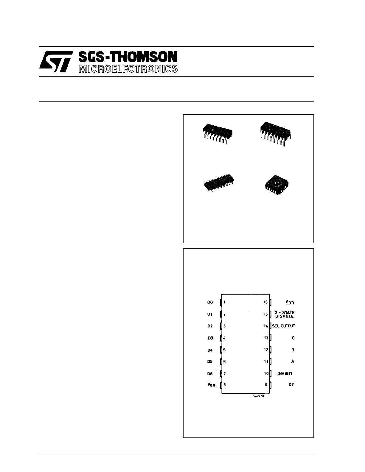
EY
(Plastic Package)
M1
(MicroPackage)
ORDERCODES :
HCC4512BF HCF4512BM1
HCF4512BEY HCF4512BC1
(CeramicPackage)
F
C1
(ChipCarrier)
DESCRIPTION
TheHCC4512B(extended temperature range) and
HCF4512B (intermediate temperature range) are
monolithic integrated circuit, available in 16-lead
dual in-line plastic or ceramic package and plastic
micro package.
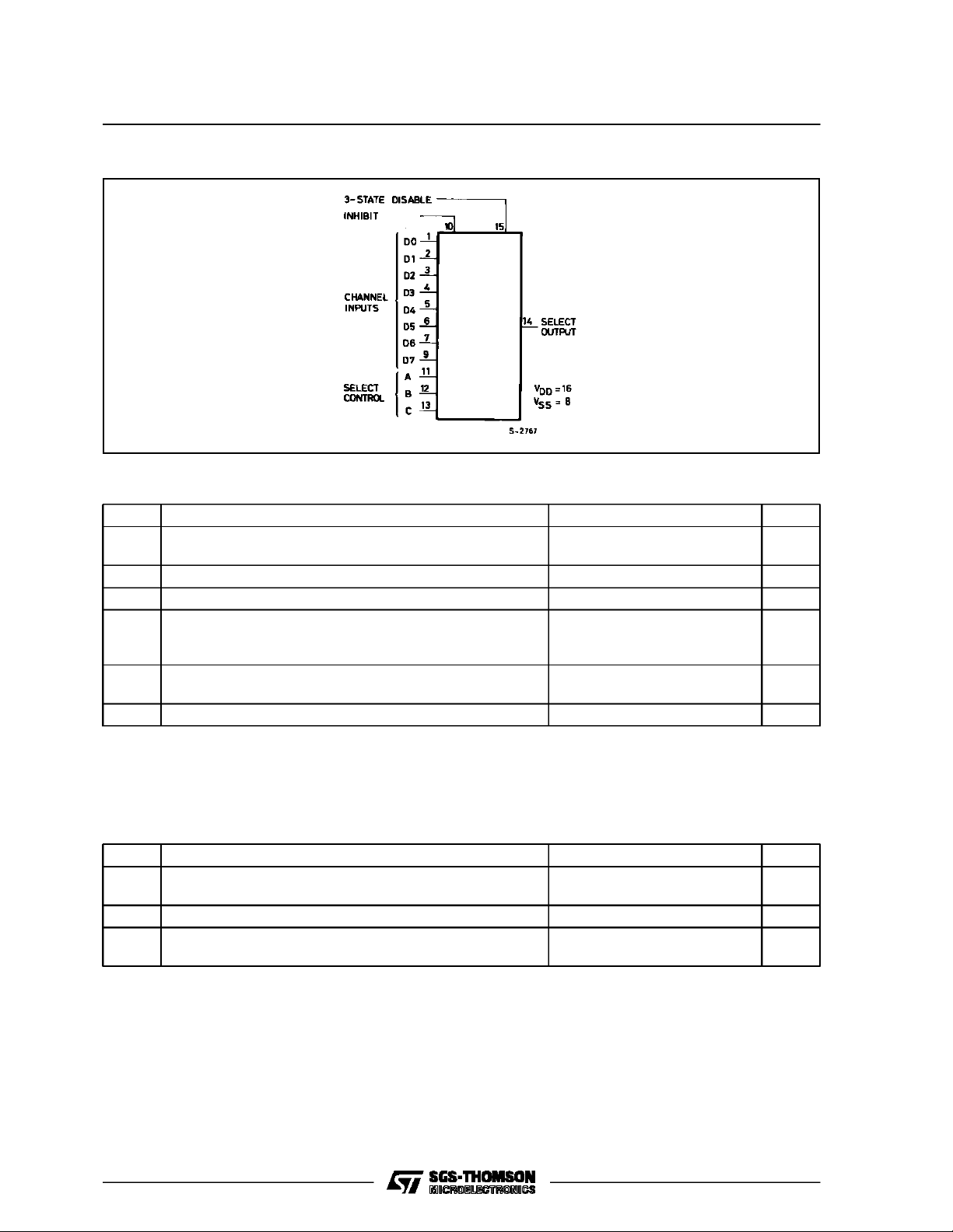
The HCC/HCF4512B is an 8-channel data selector
featuring a three-state output that can interface directlywith,anddrive,datalinesof bus-oriented systems.
PIN CON NEC TIONS
June1989
1/12
HCC/HFC4512B
FUNCTIONAL DIAGRAM
ABSOLUTE MAXIMUM RATING S
Symbol Parameter Value Unit
* Supply Voltage :HCC Types
V
DD
HCF Types
V
Input Voltage – 0.5 to VDD+ 0.5 V
i
I
DC Input Current (any one input) ± 10 mA
I
P
Total Power Dissipation (per package)
tot
Dissipation per Output Transistor
for T
T
Operating Temperature : HCC Types
op
= Full Package-temperature Range
op
HCF Types
T
Stresses above those listed under ”Absolute Maximum Ratings may cause permanent ddamage to the device. This is a stress rating only
and functionnal operation of the device at these or any other conditions above those indicated in the operationale sections of this specification is not implied. Exposure to absolute maximum rating conditions for external periods may affect device reliability.
* All voltage values are refered to VSSpin voltage.
Storage Temperature – 65 to + 150 °C
stg
– 0.5 to + 20
– 0.5 to + 18
200
100
– 55 to + 125
–40to+85
V
V
mW
mW
°C
°C
RECOMMENDED OPERATING CO NDITIONS
Symbol Parameter Value Unit
V
T
2/12
Supply Voltage : HC C Types
DD
HCF Types
V
Input Voltage 0 to V
I
Operating Temperature : HCC Types
op
HCF Types
3to+18
3to+15
DD
– 55 to + 125
–40to+85
V
V
V
°C
°C
TRUTH TABLE
HCC/HCF4512B
Sel. Cont.
ABC
000 0 0 D0
100 0 0 D1
010 0 0 D2
110 0 0 D3
001 0 0 D4
101 0 0 D5
011 0 0 D6
111 0 0 D7
XXX 1 0 0
X X X X 1 High Z
1 = High Level 0 = Low Level X = Don’t Care
Inh. 3-St ate Disable Sel. Output
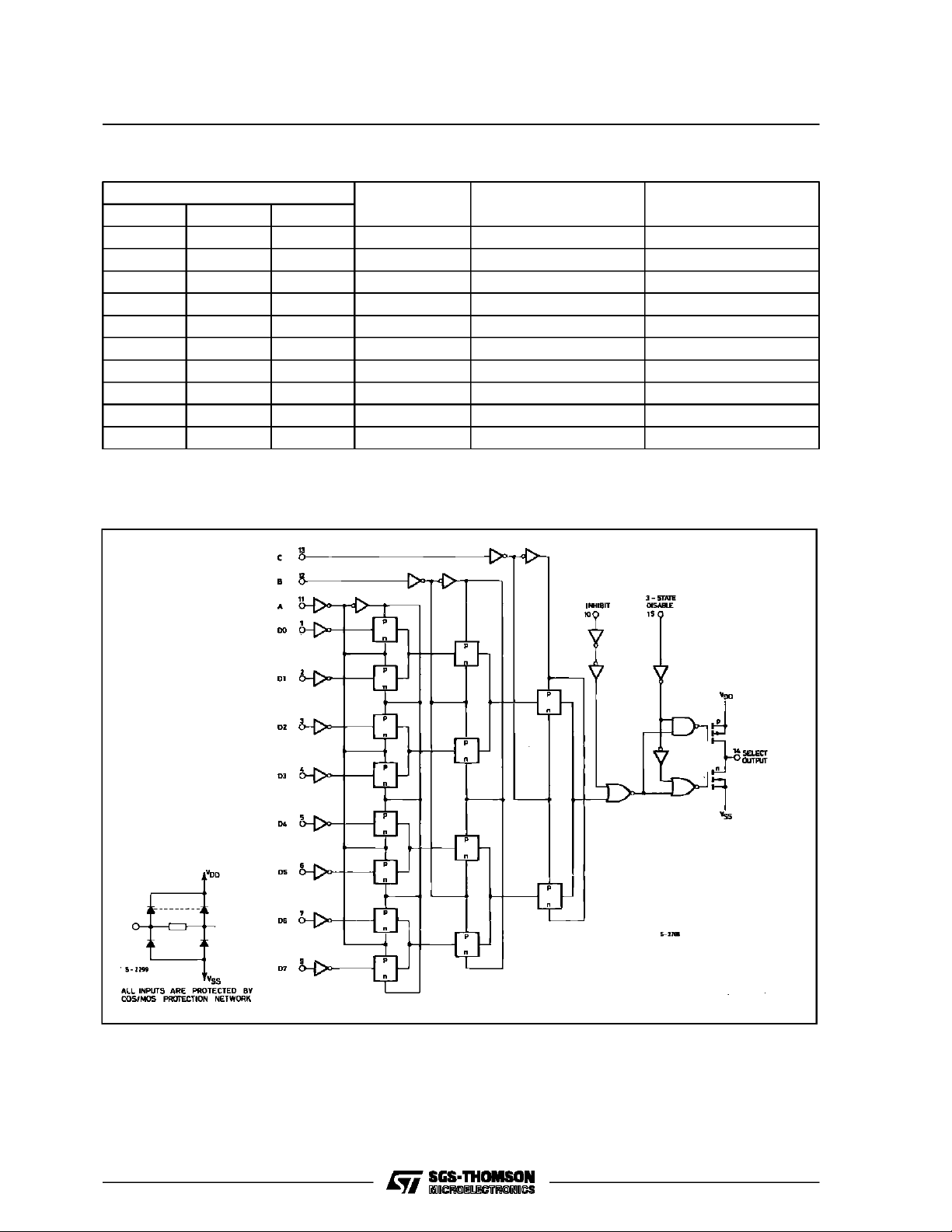
LOGIC DIAGRAMS
3/12
HCC/HFC4512B
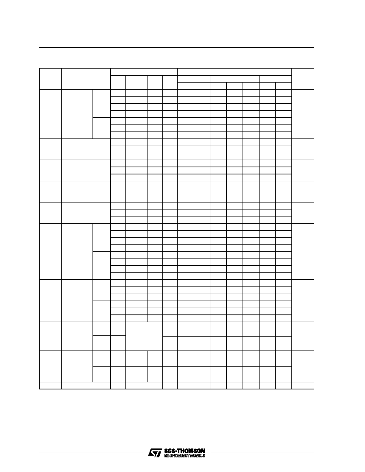
STATIC ELECTRICAL CHARACTERISTICS (over recommended operating conditions)
Test Conditions Valu e
Symbol Parameter
(V) (V) (µA) (V)
I
L
Quiescent
Current
HCC
Types
0/ 5 5 5 0.04 5 150
0/10 10 10 0.04 10 300
0/15 15 20 0.04 20 600
0/20 20 100 0.08 100 3000
0/ 5 5 20 0.04 20 150
HCF
Types
OH
Output High
V
Voltage
0/10 10 40 0.04 40 300
0/15 15 80 0.04 80 600
0/ 5 < 1 5 4.95 4.95 4.95
0/10 < 1 10 9.95 9.95 9.95
0/15 < 1 15 14.95 14.95 14.95
OL
Output Low
V
Voltage
5/0 < 1 5 0.05 0.05 0.05
10/0 < 1 10 0.05 0.05 0.05
15/0 < 1 15 0.05 0.05 0.05
IH
Input High
V
Voltage
IL
Input Low
V
Voltage
I
OH
Output
Drive
Current
HCC
Types
0/ 5 2.5 5 – 2 – 1.6 – 3.2 – 1.15
0/ 5 4.6 5 – 0.64 – 0.51 – 1 – 0.36
0/10 9.5 10 – 1.6 – 1.3 – 2.6 – 0.9
0/15 13.5 15 – 4.2 – 3.4 – 6.8 – 2.4
0/ 5 2.5 5 – 1.53 – 1.36 – 3.2 – 1.1
HCF
Types
0/ 5 4.6 5 – 0.52 – 0.44 – 1 – 0.36
0/10 9.5 10 – 1.3 – 1.1 – 2.6 – 0.9
0/15 13.5 15 – 3.6 – 3.0 – 6.8 – 2.4
OL
Output
Sink
Current
HCC
Types
I
0/ 5 0.4 5 0.64 0.51 1 0.36
0/10 0.5 10 1.6 1.3 2.6 0.9
0/15 1.5 15 4.2 3.4 6.8 2.4
0/ 5 0.4 5 0.52 0.44 1 0.36
I
IH,IIL
Input
Leakage
Current
HCF
Types
HCC
Types
0/10 0.5 10 1.3 1.1 2.6 0.9
0/15 1.5 15 3.6 3.0 6.8 2.4
0/18
HCF
0/15
Types
I
Omax
3-State
Output
Leakage
Current
HCC
Types
HCF
0/18 0/18
0/18 0/18
Types
Input Capacitance Any Input 5 7.5 pF
C
I
*T
=–55°C for HCC device : – 40°C for HCF device.
Low
*T
= + 125°C for HCC device : + 85°C for HCF device.
High
TheNoise Margin for both ”1” and ”0” level is : 1V min. with VDD= 5V,2V min.with VDD=10V, 2.5 V min. withVDD= 15V.
V
V
I
O
|IO|V
DD
T
* 25°CT
Low
Min. Max. Min. Typ. Max. Min. Max.
0.5/4.5 < 1 5 3.5 3.5 3.5
1/9 < 1 10 7 7 7
1.5/13.5 < 1 15 11 11 11
4.5/0.5 < 1 5 1.5 1.5 1.5
9/1 < 1 10 3 3 3
13.5/1.5 < 1 15 4 4 4
–5
18 ± 0.1 ±10
± 0.1 ± 1
Any Input
15 ± 0.3 ±10
18 ± 0.4 ±10
18 ± 1.0 ±10
–5
± 0.3 ± 1
–4
± 0.4 ± 12
–4
± 1.0 7.5
High
Unit
*
µA
V
V
V
V
mA
mA
µA
µA
4/12
HCC/HCF4512B
DYNAMIC ELECTRICAL CHARACTERISTICS (T
=25°C,CL= 50pF, RL= 200kΩ,
amb
typical temperature coefficient for all VDDvalues is 0.3%/°C, all input rise and fall time = 20ns)
Symbol Parameter
t
,
PHL
t
PLH
t
PHL
t
PLH
t
PHL
t
PLH
t
PZL,tPLZ
t
PHZ,tPZH
t
THL
t
TLH
Propagation Delay Time Inhibit
to Output
,
Propagation Delay Time ”A”
Select to Output
,
Propagation Delay Time
Data to Output
3-state Disable Delay Time 5 60 120
,
Transition Time 5 100 200
Test Conditions Value
V
(V) Min. Typ. Max.
DD
5140280
10 70 140
15 50 100
5200400
10 85 170
15 60 120
5180360
10 75 150
15 55 110
10 30 60
15 20 40
10 50 100
15 40 80
Unit
ns
ns
ns
ns
ns
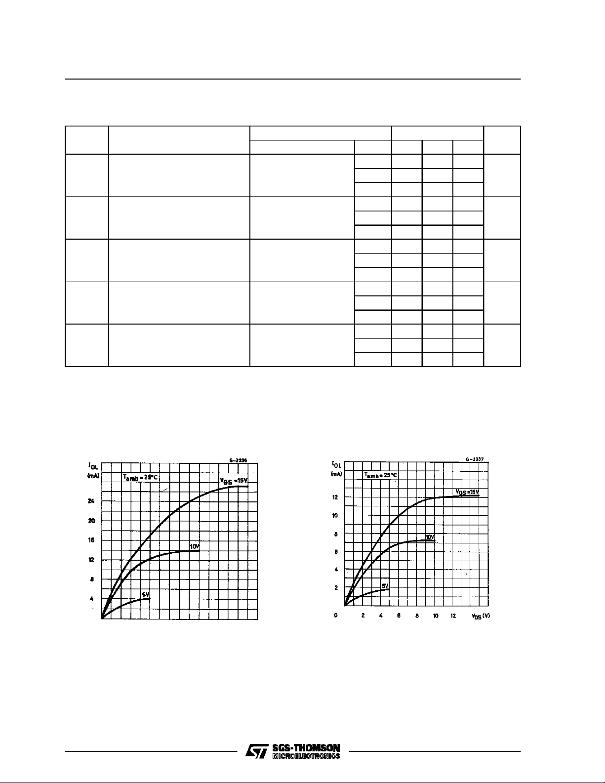
TypicalOutputLow (sink) Current Characteristics.
Minimum Output Low(sink) Current Characteristics.
5/12
HCC/HFC4512B
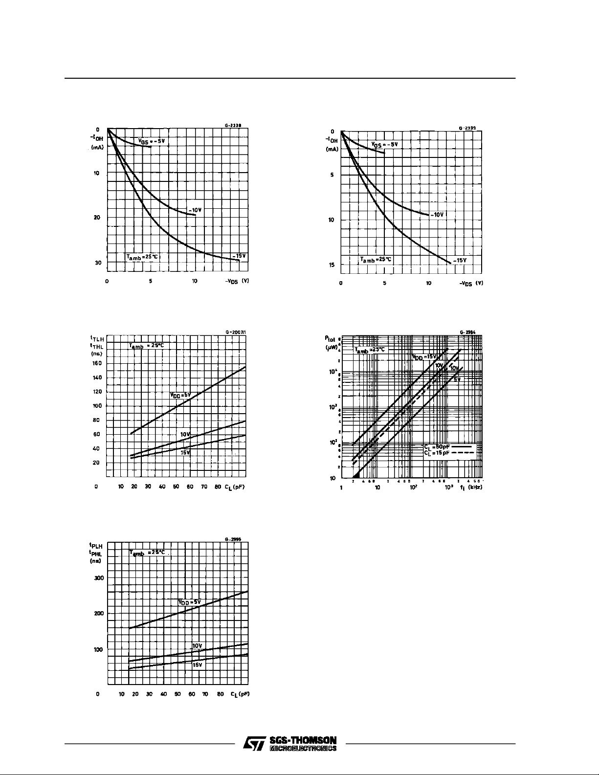
Typical OutputHigh (source)Current Characteristics.
Minimum Output High (source) Current Characteristics.
Typical Transition Time vs. Load Capacitance. Typical Dynamic Power Dissipation vs. Input Fre-
quency.
TypicalPropagation Delay Time as a Functionof
Load Capacitance (”A” select to output).
6/12

TEST CIRCUITS
HCC/HCF4512B
Dynamic PowerDissipation Test Circuit.
Input Current Test Circuit.
QuiescentDevice Current Test Circuit.
Input Voltage Test Circuit.
7/12

HCC/HFC4512B
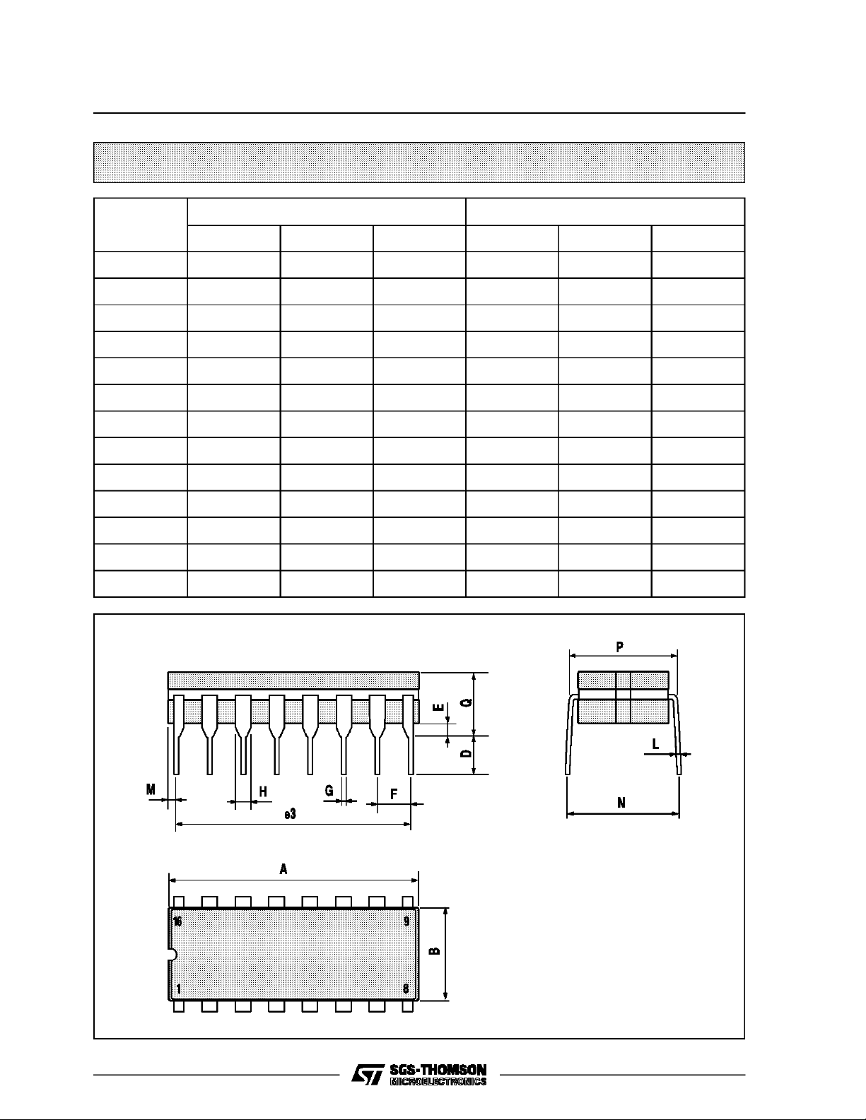
Plastic DIP16 (0.25) MECHANICAL DATA
DIM.
MIN. TYP. MAX. MIN. TYP. MAX.
a1 0.51 0.020
B 0.77 1.65 0.030 0.065
b 0.5 0.020
b1 0.25 0.010
D 20 0.787
E 8.5 0.335
e 2.54 0.100
e3 17.78 0.700
F 7.1 0.280
I 5.1 0.201
L 3.3 0.130
Z 1.27 0.050
mm inch
8/12
P001C
Ceramic DIP16/1 MECHANICAL DATA
HCC/HCF4512B
DIM.
MIN. TYP. MAX. MIN. TYP. MAX.
A 20 0.787
B 7 0.276
D 3.3 0.130
E 0.38 0.015
e3 17.78 0.700
F 2.29 2.79 0.090 0.110
G 0.4 0.55 0.016 0.022
H 1.17 1.52 0.046 0.060
L 0.22 0.31 0.009 0.012
M 0.51 1.27 0.020 0.050
N 10.3 0.406
P 7.8 8.05 0.307 0.317
Q 5.08 0.200
mm inch
P053D
9/12

HCC/HFC4512B
SO16 (Narrow) MECHANICAL DATA
DIM.
MIN. TYP. MAX. MIN. TYP. MAX.
A 1.75 0.068
a1 0.1 0.2 0.004 0.007
a2 1.65 0.064
b 0.35 0.46 0.013 0.018
b1 0.19 0.25 0.007 0.010
C 0.5 0.019
c1 45° (typ.)
D 9.8 10 0.385 0.393
E 5.8 6.2 0.228 0.244
e 1.27 0.050
e3 8.89 0.350
F 3.8 4.0 0.149 0.157
G 4.6 5.3 0.181 0.208
L 0.5 1.27 0.019 0.050
M 0.62 0.024
S8°(max.)
mm inch
10/12
P013H

PLCC20 MECHANICAL DATA
HCC/HCF4512B
DIM.
MIN. TYP. MAX. MIN. TYP. MAX.
A 9.78 10.03 0.385 0.395
B 8.89 9.04 0.350 0.356
D 4.2 4.57 0.165 0.180
d1 2.54 0.100
d2 0.56 0.022
E 7.37 8.38 0.290 0.330
e 1.27 0.050
e3 5.08 0.200
F 0.38 0.015
G 0.101 0.004
M 1.27 0.050
M1 1.14 0.045
mm inch
P027A
11/12

HCC/HFC4512B
Information furnished is believed to be accurate and reliable. However, SGS-THOMSON Microelectronics assumes no responsability for the
consequences of useof such information nor for any infringement of patents or other rights of third partieswhich may results from its use. No
license isgranted byimplication or otherwiseunder any patent or patentrights of SGS-THOMSON Microelectronics. Specificationsmentioned
in this publication are subject to changewithout notice. This publication supersedes and replaces all information previously supplied.
SGS-THOMSON Microelectronicsproductsare notauthorizedforuse ascritical componentsin life supportdevices orsystems without express
written approval of SGS-THOMSON Microelectonics.
1994 SGS-THOMSON Microelectronics - All RightsReserved
Australia - Brazil - France - Germany - Hong Kong - Italy - Japan - Korea - Malaysia - Malta - Morocco - The Netherlands -
Singapore - Spain - Sweden - Switzerland - Taiwan - Thailand - UnitedKingdom - U.S.A
SGS-THOMSON Microelectronics GROUP OF COMPANIES
12/12
 Loading...