

.SERIAL DATA INPUT - ACTIVE PARALLEL
OUTPUT
.STORAGEREGISTER CAPABILITY-MASTER
CLEAR
.CAN FUNCTIONAS DEMULTIPLEXER
.STANDARDIZED SYMMETRICAL OUTPUT
CHARACTERISTICS
.QUIESCENT CURRENT SPECIFIED TO 20V
FOR HCC DEVICE
.5V,10V,AND 15V PARAMETRIC RATINGS
.INPUT CURRENTOF100nA AT18VAND25°C
FOR HCC DEVICE
.100%TESTEDFOR QUIESCENTCURRENT
.MEETS ALLREQUIREMENTSOFJEDECTEN-
TATIVE STANDARD N°. 13A, ”STANDARD
SPECIFICATIONSFOR DESCRIPTIONOF ”B”
SERIESCMOS DEVICES”
HCC/HCF4099B
8-BIT ADDRESSABLE LATCH
EY
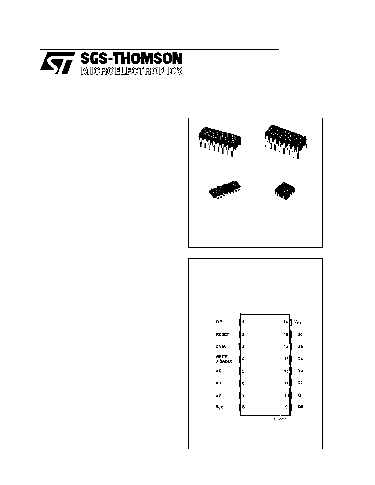
PlasticPackage
M1
MicroPackage
ORDERCODES :
HCC4099BF HCF4099BM1
HCF4099BEY HCF4099BC1
Ceramic FritSeal Package
Plastic Chip Carrier
F
C1
DESCRI PTION
TheHCC4099B (extended temperature range) and
HCF4099B (intermediate temperature range) are
monolithicintegratedcircuits,available in16-leaddual
in-line plastic or ceramic package and plastic micro
package. The HCC/HCF4099B 8-bit addressable
latchisaserial-input, parallel-output storageregister
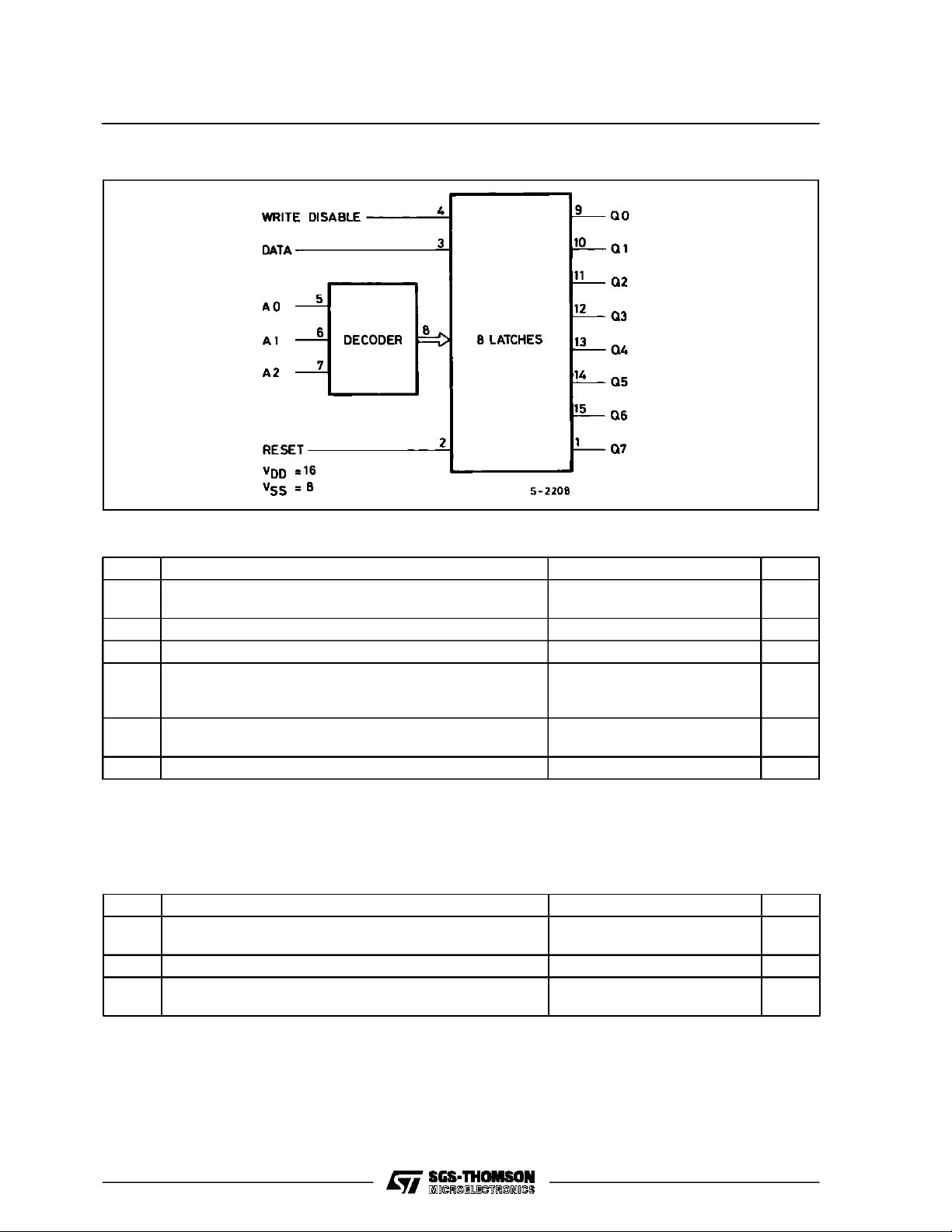
that can perform a variety of functions. Dataare inputtedto a particular bit in the latch whenthat bitis
addressed (by means of inputs A0, A1, A2) and
when WRITE DISABLE is at a low level. When
WRITE DISABLE is high, data entry is inhibited ;
however, all 8 outputscan be continuously readindependent of WRITEDISABLE andaddress inputs.
A masterRESET input is available, whichresets all
bits to a logic ”0” level when RESET and WRITE
DISABLE are at a high level.When RESETis at a
highlevel, andWRITEDISABLE is ata lowlevel,the
latch acts as a 1-of-8 demultiplexer ; the bit that is
addressed has an active output which follows the
data input, whileall unaddressed bits are held to a
logic ”0” level.
PIN CONNECTIONS
September 1988
1/14
HCC/HCF4099B
FUN CTIONAL DIAG R A M
ABSOLUTE MAXI MUM RAT IN G S
Symbol Parameter Value Unit
* Supply Voltage :HC C Types
V
DD
HCF Types
V
Input Voltage – 0.5 to VDD+ 0.5 V
i
I
DC Input Current (any one input) ± 10 mA
I
P
Total Power Dissipation (per package)
tot
– 0.5 to + 20
– 0.5 to + 18
200
V
V
mW
Dissipation per Output Transistor
for T
T
T
Stresses above listed under ”Absolute Maximum Ratings” may cause permanent damage to the device. This is a stress rating only and
functional operation of the device at these or any other conditions above those indicated in the operational sections of this specification is
not implied. Exposure to absolute maximum rating conditions for external periods may affect device reliability.
* All voltage values are referred to VSSpin voltage.
Operating Temperature : HCC Types
op
Storage Temperature – 65 to + 150 °C
stg
= Full Package-temperature Range
op
HCF Types
100
– 55 to + 125
–40to+85
mW
°C
°C
RECO MME N DED O PERA TI NG C ONDI TI ONS
Symbol Parame te r Val u e Unit
V
T
Supply Voltage : HCC Types
DD
HCF Types
V
Input Voltage 0 to V
I
Operating Temperature : HCC Types
op
HCF Types
3to 18
3to 15
DD
– 55 to + 125
–40to+85
V
V
V
°C
°C
2/14
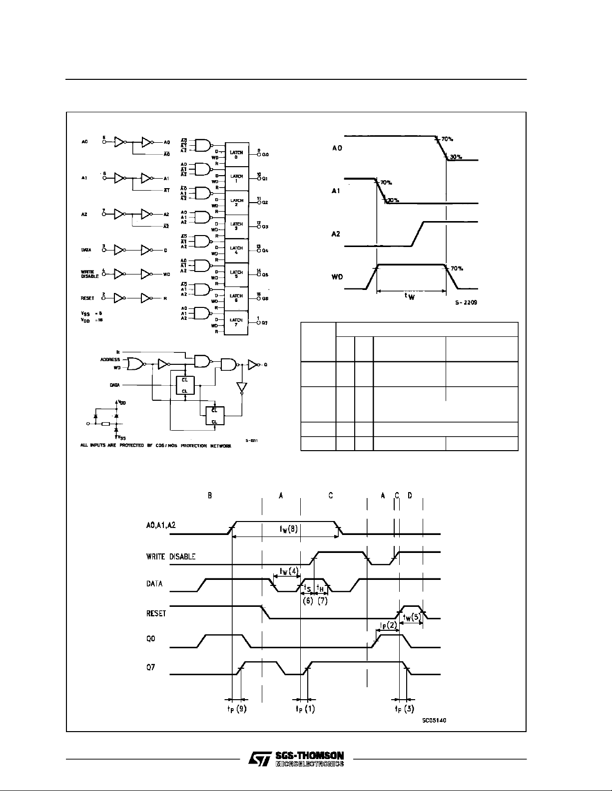
LOGI C DIAG RAM
HCC/HCF4099B
1 of 8 latches
Definition ofWRITE DIABLE ON Time
Mode Selection
Types
WD = WRITE DISABLE R = RESET
WD R
A 0 0 Follows Data Holds Previous
B 0 1 Follows Data Reset to ”0”
C 1 0 Holds Previous State
D 1 1 Reset to ”0” Reset to ”0”
Addressed
Latch
(active high 8-channel
demultiplexer)
Unad dressed
Latch
State
Master Timing Diagram
3/14

HCC/HCF4099B
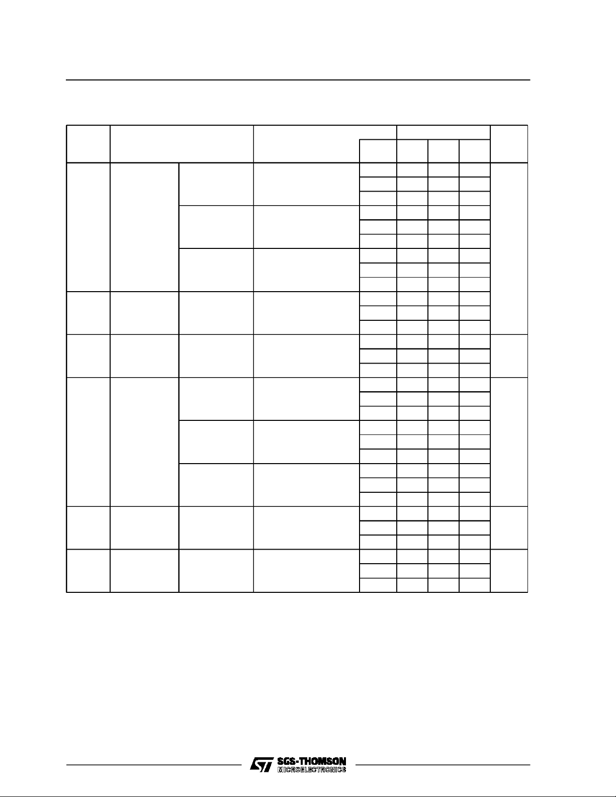
STATIC ELECTRICAL CHARACTERISTICS (over recommended operating conditions)
Test Conditions Valu e
Symbol Parameter
Quiescent
I
L
Current
HCC
Types
HCF
Types
V
OH
Output High
Voltage
V
OL
Output Low
Voltage
V
IH
Input High
Voltage
V
IL
Input Low
Voltage
I
OH
Output
Drive
Current
HCC
Types
HCF
Types
I
OL
Output
Sink
Current
HCC
Types
HCF
Types
I
IH,IIL
Input
Leakage
Current
HCC
Types
HCF
Types
Input Capacitance Any Input 5 7.5 pF
C
I
*T
=–55°C for HCC device : – 40°C for HCF device.
LOW
*T
= + 125°C for HCC device : + 85°C for HCF device.
HIGH
The Noise Margin for both ”1” and ”0” level is : 1V min. with VDD= 5V, 2V min. with VDD= 10V, 2.5V min. with VDD= 15V,
V
V
O
|IO|V
I
(V) (V) (µA) (V)
T
DD
* 25°CT
Low
Min. Max. Min. Typ. Max. Min . Max.
High
0/ 5 5 5 0.04 5 150
0/10 10 10 0.04 10 300
0/15 15 20 0.04 20 600
0/20 20 100 0.08 100 3000
0/ 5 5 20 0.04 20 150
0/10 10 40 0.04 40 300
0/15 15 80 0.04 80 600
0/ 5 < 1 5 4.95 4.95 4.95
0/10 < 1 10 9.95 9.95 9.95
0/15 < 1 15 14.95 14.95 14.95
5/0 < 1 5 0.05 0.05 0.05
10/0 < 1 10 0.05 0.05 0.05
15/0 < 1 15 0.05 0.05 0.05
0.5/4.5 < 1 5 3.5 3.5 3.5
1/9 < 1 10 7 7 7
1.5/13.5 < 1 15 11 11 11
4.5/0.5 < 1 5 1.5 1.5 1.5
9/1 < 1 10 3 3 3
13.5/1.5 < 1 15 4 4 4
0/ 5 2.5 5 – 2 – 1.6 – 3.2 – 1.15
0/ 5 4.6 5 – 0.64 – 0.51 – 1 – 0.36
0/10 9.5 10 – 1.6 – 1.3 – 2.6 – 0.9
0/15 13.5 15 – 4.2 – 3.4 – 6.8 – 2.4
0/ 5 2.5 5 – 1.53 – 1.36 – 3.2 – 1.1
0/ 5 4.6 5 – 0.52 – 0.44 – 1 – 0.36
0/10 9.5 10 – 1.3 – 1.1 – 2.6 – 0.9
0/15 13.5 15 – 3.6 – 3.0 – 6.8 – 2.4
0/ 5 0.4 5 0.64 0.51 1 0.36
0/10 0.5 10 1.6 1.3 2.6 0.9
0/15 1.5 15 4.2 3.4 6.8 2.4
0/ 5 0.4 5 0.52 0.44 1 0.36
0/10 0.5 10 1.3 1.1 2.6 0.9
0/15 1.5 15 3.6 3.0 6.8 2.4
0/18
18 ± 0.1 ±10
–5
± 0.1 ± 1
Any Input
0/15
15 ± 0.3 ±10
–5
± 0.3 ± 1
Unit
*
µA
V
V
V
V
mA
mA
µA
4/14
HCC/HCF4099B
DYNAMIC ELECTRICAL CHARACTERISTIC S(T
=25°C, CL= 50pF,RL= 200kΩ,
amb
typical temperature coefficient for all VDDvalues is0.3%/°C,all inputrise and fall times = 20ns)
Val ue
Symbol Parameter
t
PL H,tPHL
Propagation
Data to Output
Delay Time
Write Disable to
Output
Address to
Output
t
PHL
Propagation
Reset to Output
Delay Time
t
THL,tTLH
Transition
Any Output 5 100 200
Time
t
Pulse Width Data
W
Address
Reset
t
setup
Setup Time Data to Write
Disable
t
hold
Hold Time Data to Write
Disable
Test Conditions
(see master timing
diagram)
(1)
(2)
(9)
(3)
(4)
(8)
(5)
(6)
(7)
V
(V) Min. Typ. Max.
DD
5 200 400
10 75 150
15 50 100
5 200 400
10 80 160
15 60 120
5 225 450
10 100 200
15 75 150
5 175 350
10 80 160
15 65 130
10 50 100
15 40 80
5 200 100
10 100 50
15 80 40
5 400 200
10 200 100
15 125 65
515075
10 75 40
15 50 25
510050
10 50 25
15 35 20
515075
10 75 40
15 50 25
Unit
ns
ns
ns
ns
ns
5/14
 Loading...