

SGS Thomson Microelectronics HCF4067B, HCF4097B Datasheet
ANALOG MULTIPLEXER/DEMULTIPLEXER
4067B–SINGLE 16-CHANNEL
4097B–DIFFERENTIAL 8-CHANNEL
.LOW ON RESISTANCE: 125Ω (typ.) OVER 15
Vp-p SIGNAL INPUTRANGE FOR
VDD-VSS= 15V
.HIGH OFF RESISTANCE: CHANNEL LEAK-
AGE OF ±10pA(typ.) @ VDD-VSS= 10V
.MATCHED SWITCH CHARACTERISTICS:
∆RON=5Ω(typ.) FORVDD-VSS= 15V
.VERY LOW QUIESCENT POWER DISSIPA-
TION UNDER A DIGITAL CONTROL INPUT
AND SUPPLY CONDITIONS: 0.2µW (typ.) @
VDD-VSS=10V
.BINARY ADDRESSDECODING ON CHIP
.QUIESCENT CURRENT SPECIFIED TO 20V
FOR HCC DEVICE
.STANDARDIZED SYMMETRICAL OUTPUT
CHARACTERISTICS
.5V, 10V AND 15VPARAMETRIC RATINGS
.INPUT CURRENTOF 100nAAT 18V AND25
FOR HCC DEVICE
o
C
.100% TESTED FOR QUIESCENTCURRENT
.MEETSALLREQUIREMENTSOFJEDECTEN-
TATIVE STANDARD No 13A, ”STANDARD
SPECIFICATIONS FOR DESCRIPTION OF B
SERIECMOS DEVICES”
HCC/H CF 4 067 B
HCC/HCF4097B
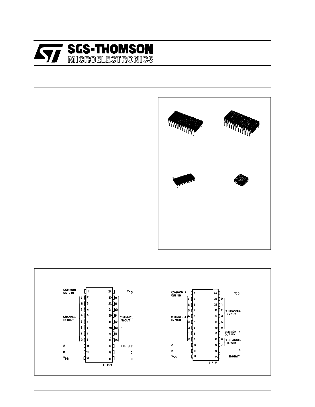
EY
(PlasticPackage)
M1
(MicroPackage)
ORDER CODES :
HCC4 0XX BF HCF40XXBM 1
HCF40XXBEY HCF40XXBC1
(CeramicPackage)
(Chip Carrier)
F
C1
PIN CONNECTIONS
September 1988
4067B 4097B
1/16
HCC/H CF4067B HC C/ HCF4097B
DESCRIPTION
The HCC4067B, HCC4097B (extended temperaturerange) andHCF4067B,HCF4097B (intermedi-
ate temperature range) are monolithic integrated
circuitsavailable in24-lead dual in lineplastic or ceramic package.
The HCC/HCF4067B and HCC/HCF4097B
COS/MOS analog multiplexers/demultiplexers are
digitally controlled analog switches having low ON
impedance, low OFF leakage current and internal
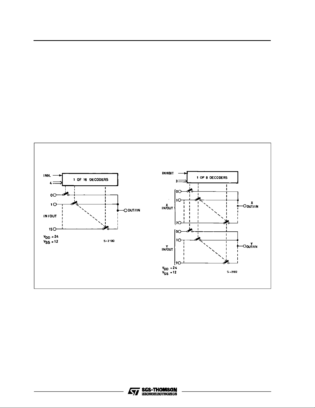
FUN CTIONAL DIAG R A M
For 4067B For 4097B
addressdecoding. in addition, the ON resistanceis
relatively constantover thefull input-signalrange.
The HCC/HCF4067B ia a 16-channel multiplexer
with fourbinary control inputs A, B, C, D, and an inhibit input,arranged so thatany combination of the
inputs selectsone switch.
TheHCC/HCF4097isa differential 8-channel multiplexerhaving threebinarycontrolinputsA,B,C,and
an inhibit input. The inputs permit selection of one
2/16
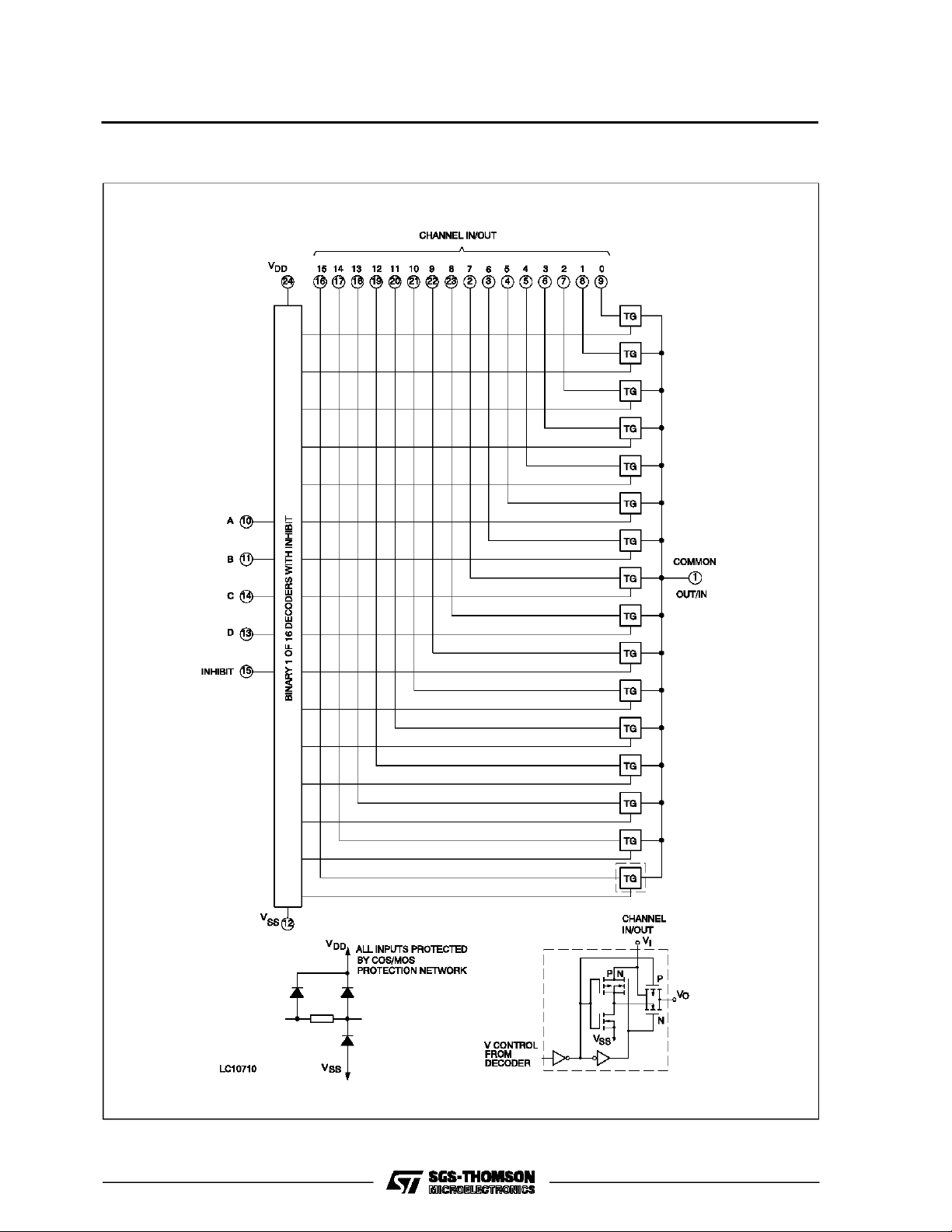
LOGI C DIAGRAM
HCC/HCF4067B HCC/HCF4097B
For 4067B
3/16
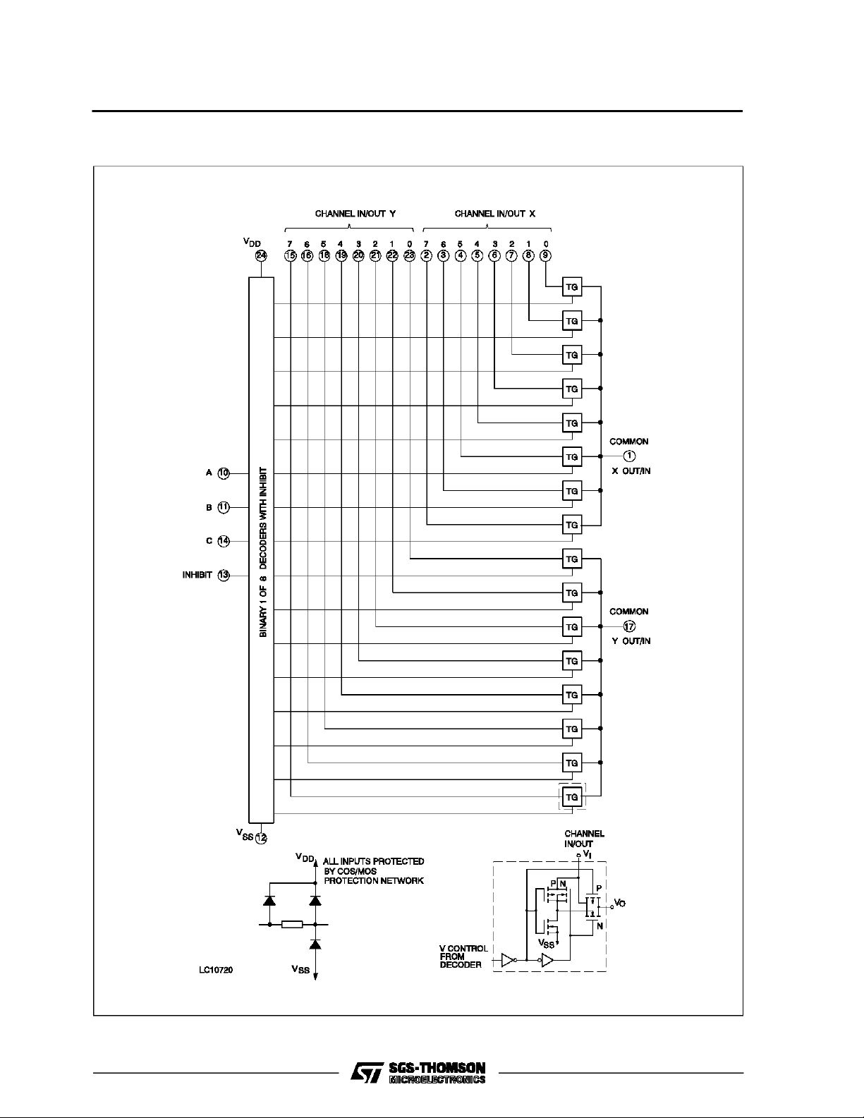
HCC/H CF4067B HC C/ HCF4097B
LOGI C DIAGRAM
For 4097B
4/16
HCC/HCF4067B HCC/HCF4097B
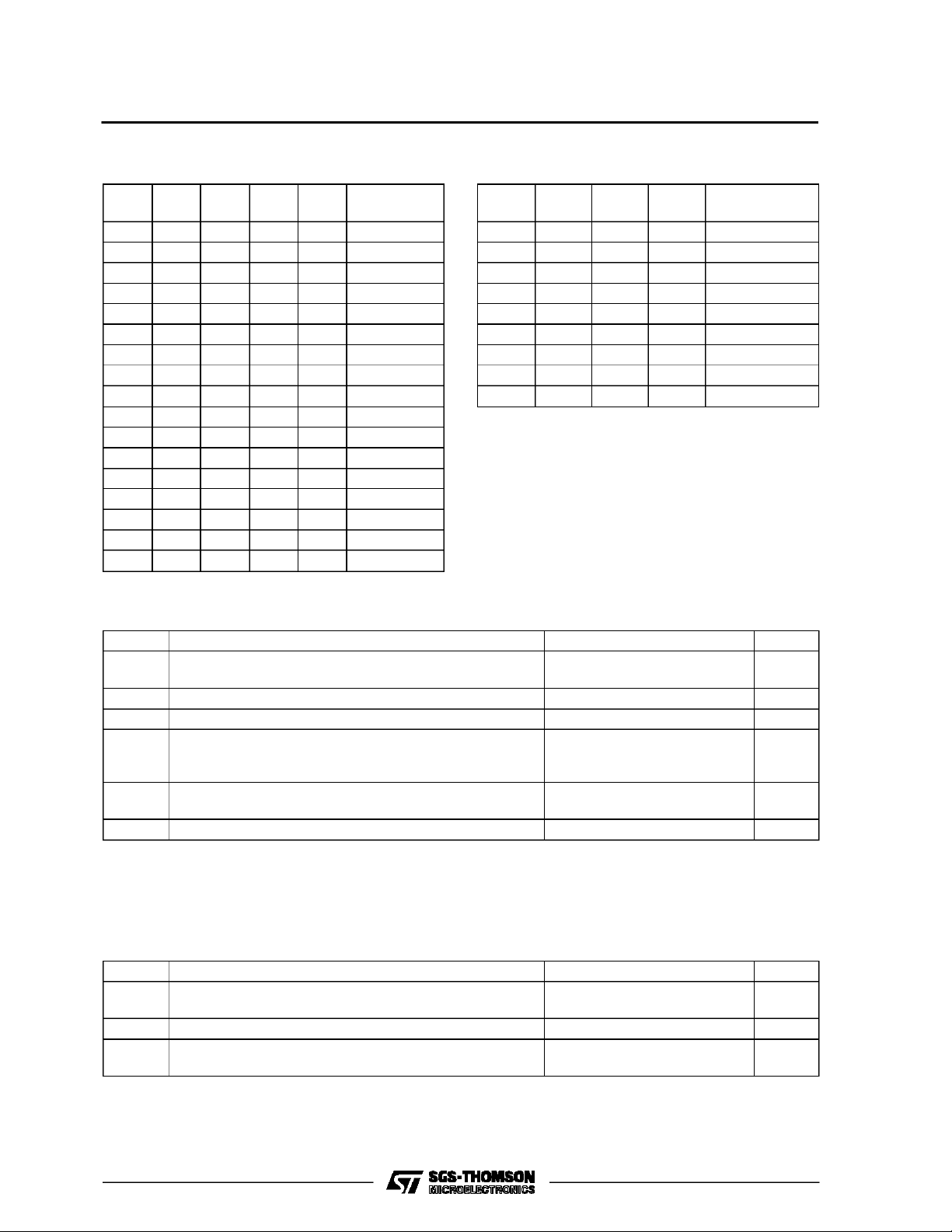
TRUTH TABLES FOR HCC/HCF4067B
A B C D INH
X X X X 1 None
00000 0
10000 1
01000 2
11000 3
00100 4
10100 5
01100 6
11100 7
00010 8
10010 9
01010 10
11010 11
00110 12
10110 13
01110 14
11110 15
SELECTED
CHANNEL
ABSOLU TE MAXI MUM R AT ING
TRUTH TABLE FOR HCC/HCF4097B
A B C INH
X X X 1 None
0000 0X0Y
1000 1X1Y
0100 2X2Y
1100 3X3Y
0010 4X4Y
1010 5X5Y
0110 6X6Y
1110 7X7Y
SELECTED
CHANNEL
Symbol Parameter Value Unit
V
* Supply Voltage: HCC Types
DD
HCF Types
V
P
Input Voltage -0.5 to VDD+ 0.5 V
i
I
DC Input Current (any one input) ± 10 mA
I
Total Power Dissipation (per package)
tot
-0.5 to +20
-0.5 to +18
200
V
V
mW
Dissipation per Output Transistor
for Top = Full Package Temperature Range
T
Operating Temperature: HCC Types
op
HCF Types
T
Stressesabove thoselistedunder ”AbsoluteMaximum Ratings”maycausepermanent damage to thedevice. Thisisa stressratingonlyand functional
operation of the device at these or any otherconditionsabove thoseindicated in theoperational sections of thisspecification isnotimplied.Exposure
to absolute maximum ratingconditions forexternal periods may affectdevice reliability.
* All voltagevalues arereferred to VSSpinvoltage.
Storage Temperature -65 to +150
stg
100
-55 to +125
-40 to +85
mW
o
C
o
C
o
C
RECO MM ENDED OPERATI N G CONDITI ONS
Symbol Parameter Value Unit
V
V
T
Supply Voltage: HCC Types
DD
HCF Types
Input Voltage 0 to V
I
Operating Temperature: HCC Types
op
HCF Types
3to18
3to15
DD
-55 to +125
-40 to +85
V
V
V
o
C
o
C
5/16
 Loading...