

HCC/H CF 4 095 B
HCC/HCF4096B
GATEJ-K MASTER-SLAVEFLIP-FLOPS
.16 MHzTOGGLERATE (typ.) AT
VDD-VSS= 10V
.GATED INPUTS
.QUIESCENT CURRENT SPECIFIED TO 20v
FOR HCC DEVICE
.5V, 10VAND 15V PARAMETRIC RATINGS
.INPUT CURRENTOF100nA AT18VAND 25oC
FOR HCC DEVICE
.100% TESTED FOR QUIESCENTCURRENT
.MEETSALLREQUIREMENTSOFJEDECTEN-
TATIVE STANDARD No 13 A, ”STANDARD
SPECIFICATIONS FOR DESCRIPTION OF B
SERIESCMOS DEVICES”
DESCRIPTION
The HCC4095B/4096B (extended temperature
range) and HCF4095B/4096B (intermediate tem-
perature range) are monolithic integrated circuits,
available in 14 lead dual in-line plastic or ceramic
package andplastic micropackage.
TheHCC/HCF4095B andHCC/HCF4096B areJ-K
Master-Slave Flip-Flops featuring separate AND
gatingofmultipleJ andKinputs. Thegated J-Kinput
control transfer of information into the master sectionduring clockedoperation. Informationonthe J-K
inputs is transferred to the Q and Q outputson the
positive edge of the clock pulse. SET and RESET
inputs (active high) are provided for asynchronous
operation.
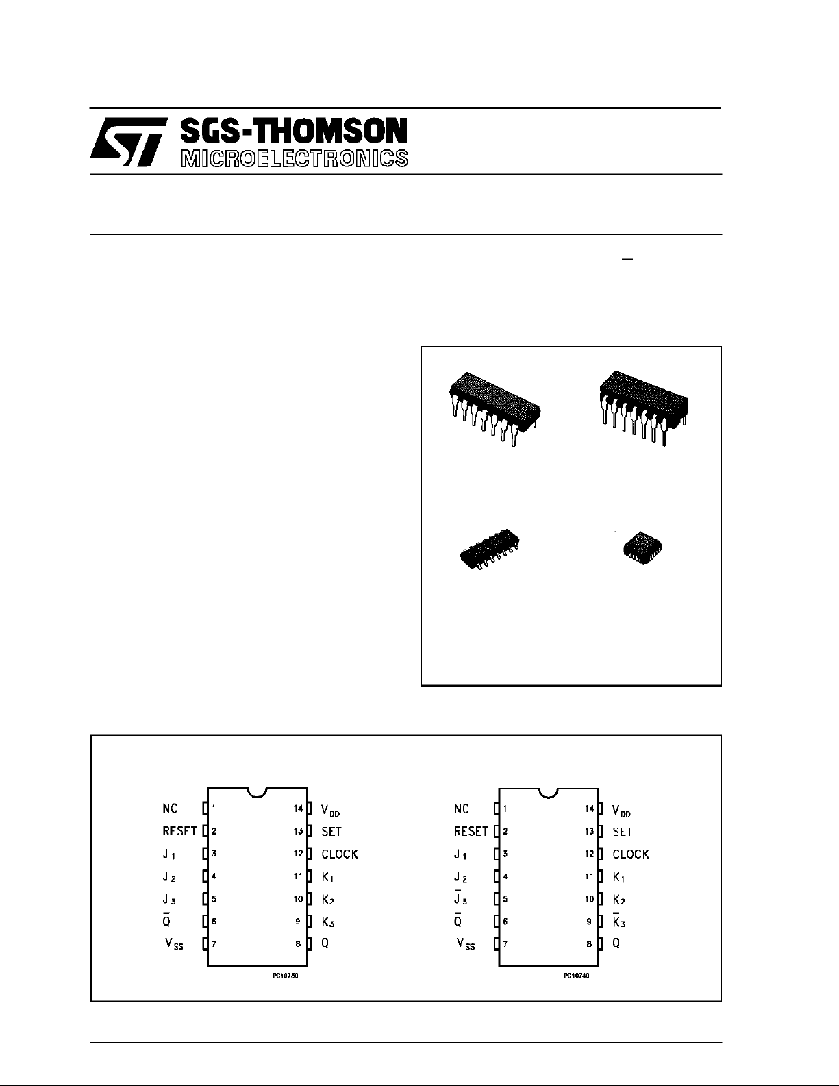
EY
(PlasticPackage)
M1
(MicroPackage)
ORDER CODES :
HCC4 0XX BF HCF40XXBM 1
HCF40XXBEY HCF40XXBC1
(CeramicPackage)
F
C1
(Chip Carrier)
PIN CONNECTIONS
September 1988
4095B 4096B
1/13
HCC/H CF4095B HC C/ HCF4096B
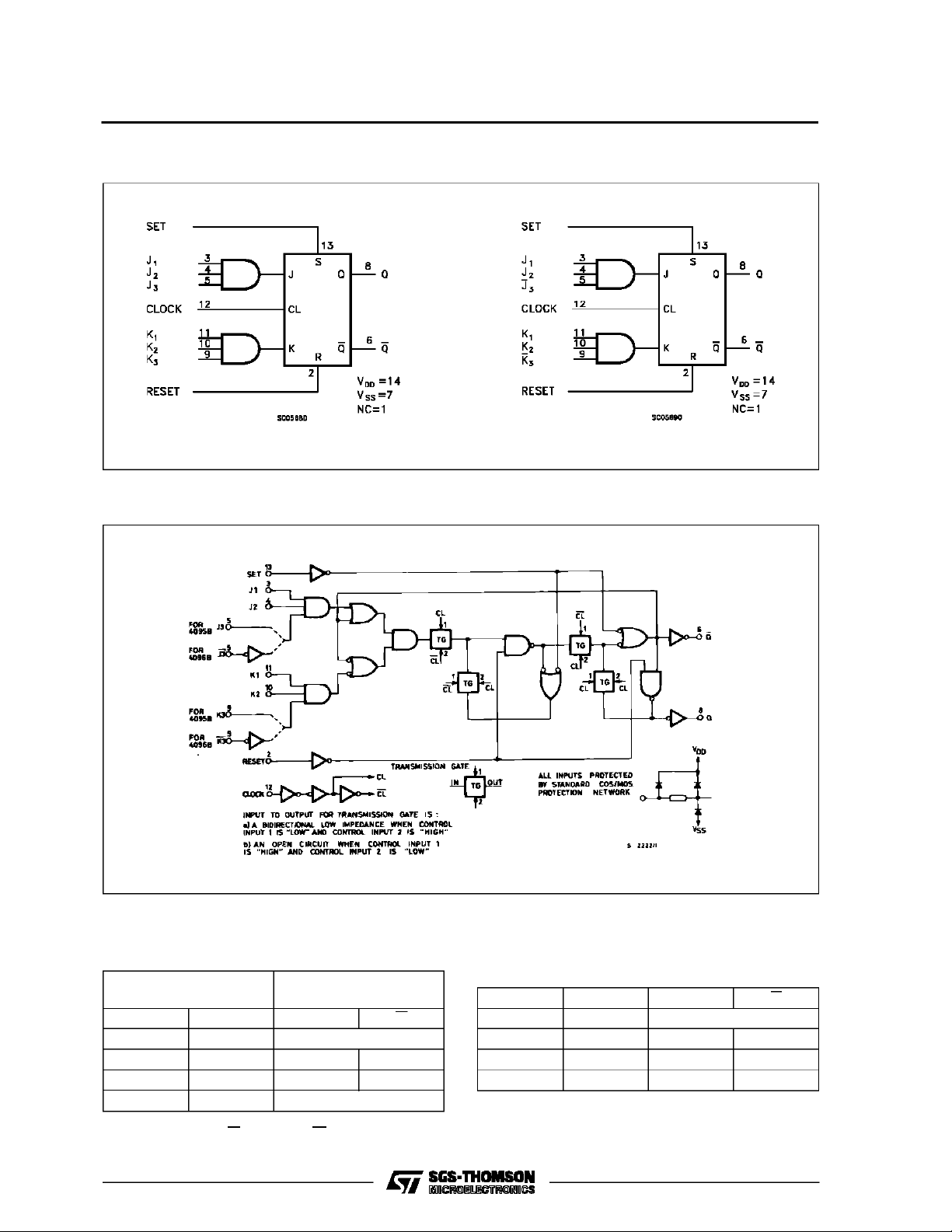
FUN CTIONAL DIAGR A MS
LOGI C DIAGRAM
TRUTH TABLES
SYNCHR ON O US OPERATI O N (S=0 R=0)
Inputs Before Positive
Clock Transition
J* K* Q Q
0 0 No Change
0101
1010
1 1 Toggles
* For 4095B J= J1 •J2 •J3,K= K1 •K2 •K3
* For 4095B J= J1 •J2 •J3,K= K1 •K2 •K3
2/13
Outputs After Positive
Clock Transition
ASYNCHRONOUS OPERATION (J and K
DON’T CARE)
SRQQ
0 0 No Change
0101
1010
1100
0=VSS,1=V
DD

HCC/HCF4095B HCC/HCF4096B
ABSOLU TE M AXI MU M R AT ING
Symbol Parameter Value Unit
V
* Supply Voltage: HCC Types
DD
HCF Types
V
P
Input Voltage -0.5 to VDD+ 0.5 V
i
I
DC Input Current (any one input) ± 10 mA
I
Total Power Dissipation (per package)
tot
Dissipation per Output Transistor
for Top = Full Package Temperature Range
T
Operating Temperature: HCC Types
op
HCF Types
T
Stressesabove thoselistedunder ”AbsoluteMaximumRatings”maycausepermanent damage tothedevice. Thisisastressratingonlyandfunctional
operation of the device atthese oranyotherconditions above thoseindicated in theoperational sections of thisspecification is not implied.Exposure
to absolute maximum ratingconditions forexternal periodsmay affectdevice reliability.
* All voltagevalues are referred toVSSpinvoltage.
Storage Temperature -65 to +150
stg
RECO MM ENDED O PERAT IN G CONDI TI O NS
Symbol Parameter Value Unit
V
V
T
Supply Voltage: HCC Types
DD
HCF Types
Input Voltage 0 to V
I
Operating Temperature: HCC Types
op
HCF Types
-0.5 to +20
-0.5 to +18
200
100
-55 to +125
-40 to +85
3to18
3to15
DD
-55 to +125
-40 to +85
V
V
mW
mW
o
C
o
C
o
C
V
V
V
o
C
o
C
3/13
HCC/H CF4095B HC C/ HCF4096B
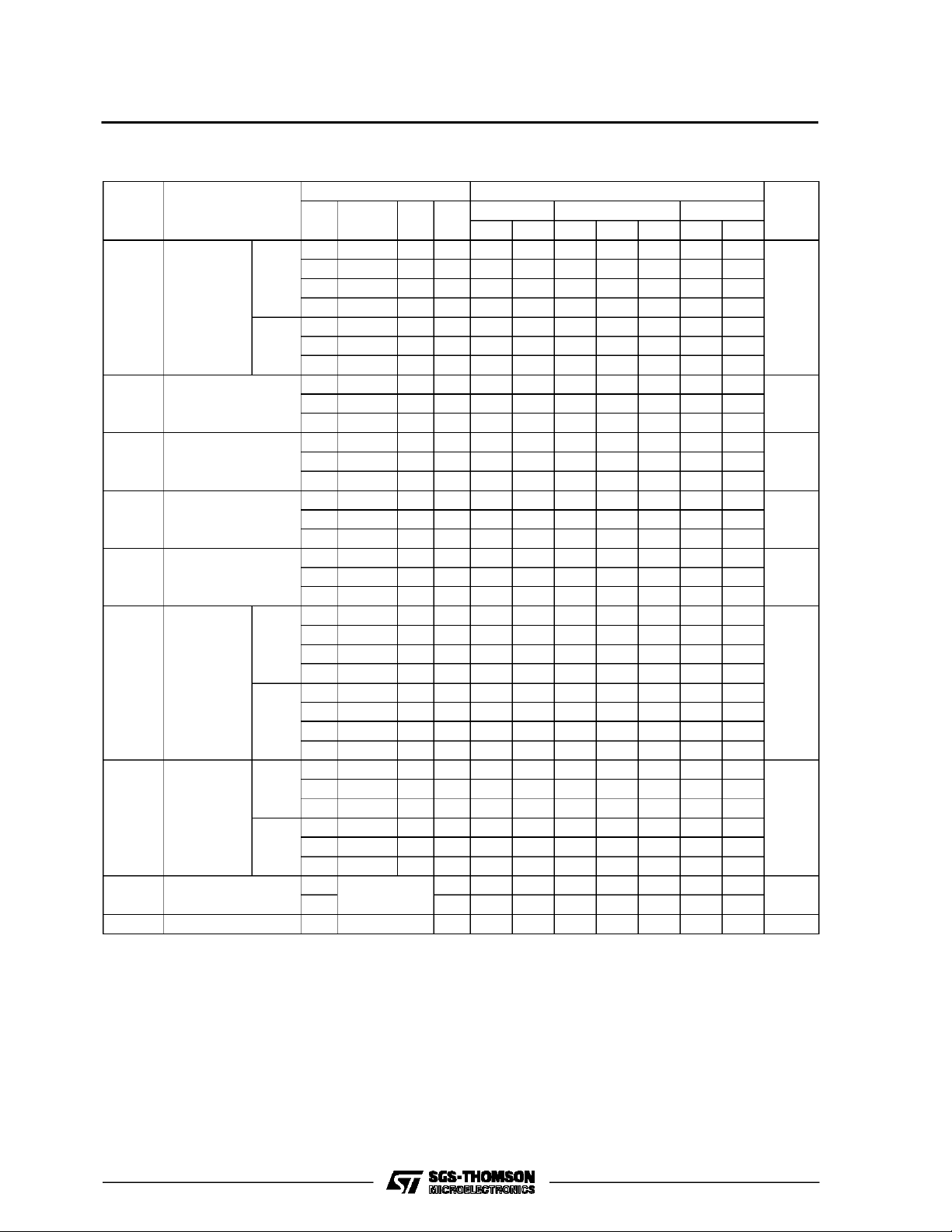
STATI C E LECT RIC AL CHAR ACTER I STI CS (over rec omm ended o pera t ing co nditions )
Test Conditios Value
Symbol Parameter
I
Quiescent
L
Current
HCC
Types
V
(V)
V
I
(V)
|IO|
(µA)
V
(V)
O
T
DD
*25
LOW
Min. Max. Min. Typ. Max. Min. Max.
0/5 5 1 0.02 1 30
0/10 10 2 0.02 2 60
0/15 15 4 0.02 4 120
o
CT
0/20 20 20 0.04 20 600
HCF
Types
0/5 5 4 0.02 4 30
0/10 10 8 0.02 8 60
0/15 15 16 0.02 16 120
OH
Output High
V
Voltage
0/5 < 1 5 4.95 4.95 4.95
0/10 < 1 10 9.95 9.95 9.95
0/15 < 1 15 14.95 14.95 14.95
V
OL
Output Low
Voltage
5/0 < 1 5 0.05 0.05 0.05
10/0 < 1 10 0.05 0.05 0.05
15/0 < 1 15 0.05 0.05 0.05
V
IH
Input High
Voltage
4.5 < 1 5 3.5 3.5 3.5
9<1107 7 7
13.5 < 1 15 11 11 11
V
IL
Input Low
Voltage
0.5 < 1 5 1.5 1.5 1.5
1<110 3 3 3
1.5 < 1 15 4 4 4
I
OH
Output
Drive
Current
HCC
Types
0/5 2.5 5 -2 -1.6 -3.2 -1.15
0/5 4.6 5 -0.64 -0.51 -1 -0.36
0/10 9.5 10 -1.6 -1.3 -2.6 -0.9
0/15 13.5 15 -4.2 -3.4 -6.8 -2.4
0/5 2.5 5 -1.53 -1.36 -3.2 -1.1
HCF
Types
0/5 4.6 5 -0.52 -0.44 -1 -0.36
0/10 9.5 10 -1.3 -1.1 -2.6 -0.9
0/15 13.5 15 -3.6 -3.0 -6.8 -2.4
I
OL
Output
Sink
Current
HCC
Types
HCF
Types
0/5 0.4 5 0.64 0.51 1 0.36
0/10 0.5 10 1.6 1.3 2.6 0.9
0/15 1.5 15 4.2 3.4 6.8 2.4
0/5 0.4 5 0.52 0.44 1 0.36
0/10 0.5 10 1.3 1.1 2.6 0.9
0/15 1.5 15 3.6 3.0 6.8 2.4
I
IH,IIL
C
*T
LOW
*T
HIGH
TheNoiseMargin for both”1” and”0” levelis: 1Vmin.withVDD=5V, 2V min.withVDD=10 V,2.5 Vmin. withVDD=15V
Input Leakage
Current
Input Capacitance Any Input 5 7.5 pF
I
=-55oCforHCCdevice: -40oC for HCF device.
=+125oCforHCC device: +85oC for HCF device.
0/18
0/15 15 ±0.3 ±10
Any Input
18 ±0.1 ±10-5±0.1 ±1
-5
±0.3 ±1
HIGH
Unit
*
µA
V
V
V
V
mA
mA
µA
4/13

HCC/HCF4095B HCC/HCF4096B
DYNAMIC ELECTRICAL CHARACTERISTICS (T
=25oC, CL=50pF,RL= 200 KΩ,
amb
typic al temperat ur e coef f i c en t for all VDDvalues is 03 %/oC, all input ris e and f al l t im es = 20 ns)
Symbol Parameter
t
PLH
t
PHL
t
PLH
t
PHL
t
THL
t
TLH
f
t
t
rtf
t
t
setup
Propagation Delay Time 5 250 500
Propagation Delay Time
(Set or Reset)
Transition Time 5 100 200
Maximum Clock Input Frequency 5 3.5 7
CL
Clock Pulse Width 5 140 70
W
Clock Input Rise or Fall Time 5 15
Set or Reset Pulse Width 5 200 100
W
Data Setup Time 5 400 200
Test Conditions Value
(V) Min. Typ. Max.
V
DD
10 100 200
15 75 150
5 150 300
10 75 150
15 50 100
10 50 100
15 40 80
10 8 16
15 12 24
10 60 30
15 40 20
10 5
15 5
10 100 50
15 50 25
10 160 80
15 100 50
Unit
ns
ns
ns
MHz
ns
µs
ns
ns
Typical Output Low (sink) Current Characteristics Minimum Output low (sink) Current Charac-
teristics
5/13

HCC/H CF4095B HC C/ HCF4096B
Typical Output High (source) Current Characteristics
Typical Propagation Delay Time vs Load Capacitance
Minimum Output High (source) Current Characteristics
Typical Transition Time vs Load Capacitance
Typical Clock Frequency vs Supply Voltage
(Toggle Mode)
6/13
Typical Power Power Dissipation Vs. Input Clock
Frequency

HCC/HCF4095B HCC/HCF4096B
TYPICAL APPLI CA TI O NS
T-type Flip-Flop D-type Flip-Flop
Synchronous Binary Divide by Ten Counter
STATE QA QB QC QD
00000
11000
20100
31100
40010
51010
60110
71110
80001
91001
NOTE:Inall4095B unitstheSetand Reset areConnected toV
SS
7/13

HCC/H CF4095B HC C/ HCF4096B
WAV EFORMS
Propagation Delay, Transition and Setup Time Clock Pulse Rise and Fall Time
TEST CIRCUITS
QuiescentDevice Current. Noise Immunity.
Input Leakage Current.
8/13

HCC/HCF4095B HCC/HCF4096B
Plastic DIP14 MECHANICAL DATA
DIM.
MIN. TYP. MAX. MIN. TYP. MAX.
a1 0.51 0.020
B 1.39 1.65 0.055 0.065
b 0.5 0.020
b1 0.25 0.010
D 20 0.787
E 8.5 0.335
e 2.54 0.100
e3 15.24 0.600
F 7.1 0.280
I 5.1 0.201
L 3.3 0.130
Z 1.27 2.54 0.050 0.100
mm inch
P001A
9/13

HCC/H CF4095B HC C/ HCF4096B
Ceramic DIP14/1 MECHANICAL DATA
DIM.
MIN. TYP. MAX. MIN. TYP. MAX.
A 20 0.787
B 7.0 0.276
D 3.3 0.130
E 0.38 0.015
e3 15.24 0.600
F 2.29 2.79 0.090 0.110
G 0.4 0.55 0.016 0.022
H 1.17 1.52 0.046 0.060
L 0.22 0.31 0.009 0.012
M 1.52 2.54 0.060 0.100
N 10.3 0.406
P 7.8 8.05 0.307 0.317
Q 5.08 0.200
mm inch
10/13
P053C

HCC/HCF4095B HCC/HCF4096B
SO14 MECHANICAL DATA
DIM.
MIN. TYP. MAX. MIN. TYP. MAX.
A 1.75 0.068
a1 0.1 0.2 0.003 0.007
a2 1.65 0.064
b 0.35 0.46 0.013 0.018
b1 0.19 0.25 0.007 0.010
C 0.5 0.019
c1 45° (typ.)
D 8.55 8.75 0.336 0.344
E 5.8 6.2 0.228 0.244
e 1.27 0.050
e3 7.62 0.300
F 3.8 4.0 0.149 0.157
G 4.6 5.3 0.181 0.208
L 0.5 1.27 0.019 0.050
M 0.68 0.026
S8°(max.)
mm inch
P013G
11/13

HCC/H CF4095B HC C/ HCF4096B
PLCC20 MECHANICAL DATA
DIM.
MIN. TYP. MAX. MIN. TYP. MAX.
A 9.78 10.03 0.385 0.395
B 8.89 9.04 0.350 0.356
D 4.2 4.57 0.165 0.180
d1 2.54 0.100
d2 0.56 0.022
E 7.37 8.38 0.290 0.330
e 1.27 0.050
e3 5.08 0.200
F 0.38 0.015
G 0.101 0.004
M 1.27 0.050
M1 1.14 0.045
mm inch
12/13
P027A

HCC/HCF4095B HCC/HCF4096B
Information furnished is believed tobe accurate and reliable. However, SGS-THOMSON Microelectronics assumes no responsability for the
consequences of use of such information nor for any infringement of patents or other rights of third parties which may results from its use. No
license is granted byimplication orotherwiseunderany patentor patentrights ofSGS-THOMSON Microelectronics. Specificationsmentioned
in this publication are subject to change without notice. Thispublication supersedes and replaces all information previously supplied.
SGS-THOMSON Microelectronicsproducts are not authorized foruse ascritical componentsinlife support devices or systems without express
written approval of SGS-THOMSON Microelectonics.
1994 SGS-THOMSON Microelectronics- All Rights Reserved
Australia - Brazil - France - Germany - HongKong - Italy - Japan - Korea - Malaysia - Malta - Morocco - The Netherlands -
Singapore -Spain - Sweden - Switzerland - Taiwan - Thailand - United Kingdom - U.S.A
SGS-THOMSON Microelectronics GROUP OF COMPANIES
13/13
 Loading...