

SGS Thomson Microelectronics HCF4096B, HCF4095B Datasheet
HCC/H CF 4 095 B
HCC/HCF4096B
GATEJ-K MASTER-SLAVEFLIP-FLOPS
.16 MHzTOGGLERATE (typ.) AT
VDD-VSS= 10V
.GATED INPUTS
.QUIESCENT CURRENT SPECIFIED TO 20v
FOR HCC DEVICE
.5V, 10VAND 15V PARAMETRIC RATINGS
.INPUT CURRENTOF100nA AT18VAND 25oC
FOR HCC DEVICE
.100% TESTED FOR QUIESCENTCURRENT
.MEETSALLREQUIREMENTSOFJEDECTEN-
TATIVE STANDARD No 13 A, ”STANDARD
SPECIFICATIONS FOR DESCRIPTION OF B
SERIESCMOS DEVICES”
DESCRIPTION
The HCC4095B/4096B (extended temperature
range) and HCF4095B/4096B (intermediate tem-
perature range) are monolithic integrated circuits,
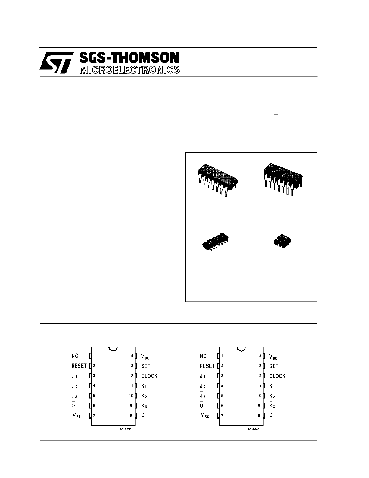
available in 14 lead dual in-line plastic or ceramic
package andplastic micropackage.
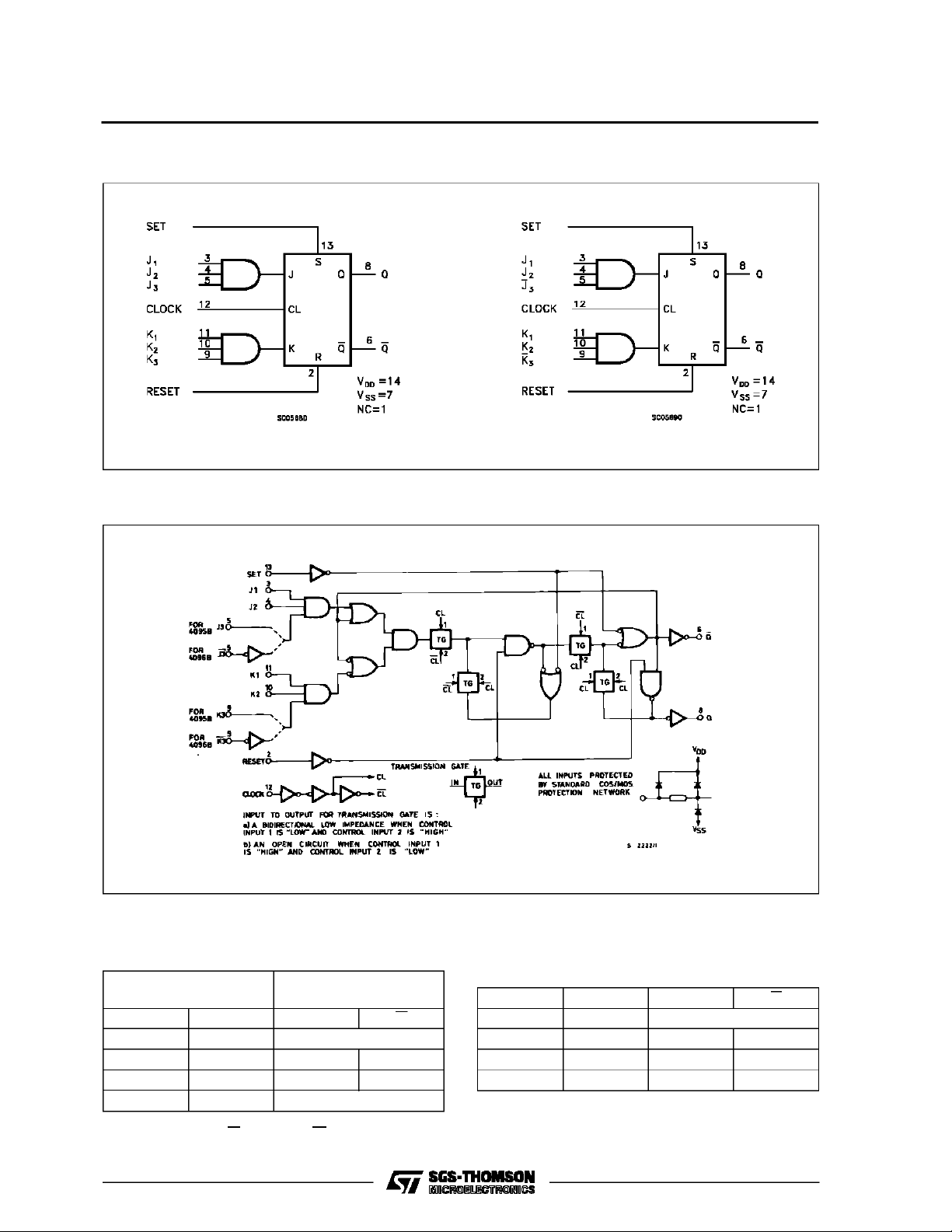
TheHCC/HCF4095B andHCC/HCF4096B areJ-K
Master-Slave Flip-Flops featuring separate AND
gatingofmultipleJ andKinputs. Thegated J-Kinput
control transfer of information into the master sectionduring clockedoperation. Informationonthe J-K
inputs is transferred to the Q and Q outputson the
positive edge of the clock pulse. SET and RESET
inputs (active high) are provided for asynchronous
operation.
EY
(PlasticPackage)
M1
(MicroPackage)
ORDER CODES :
HCC4 0XX BF HCF40XXBM 1
HCF40XXBEY HCF40XXBC1
(CeramicPackage)
F
C1
(Chip Carrier)
PIN CONNECTIONS
September 1988
4095B 4096B
1/13
HCC/H CF4095B HC C/ HCF4096B
FUN CTIONAL DIAGR A MS
LOGI C DIAGRAM
TRUTH TABLES
SYNCHR ON O US OPERATI O N (S=0 R=0)
Inputs Before Positive
Clock Transition
J* K* Q Q
0 0 No Change
0101
1010
1 1 Toggles
* For 4095B J= J1 •J2 •J3,K= K1 •K2 •K3
* For 4095B J= J1 •J2 •J3,K= K1 •K2 •K3
2/13
Outputs After Positive
Clock Transition
ASYNCHRONOUS OPERATION (J and K
DON’T CARE)
SRQQ
0 0 No Change
0101
1010
1100
0=VSS,1=V
DD

HCC/HCF4095B HCC/HCF4096B
ABSOLU TE M AXI MU M R AT ING
Symbol Parameter Value Unit
V
* Supply Voltage: HCC Types
DD
HCF Types
V
P
Input Voltage -0.5 to VDD+ 0.5 V
i
I
DC Input Current (any one input) ± 10 mA
I
Total Power Dissipation (per package)
tot
Dissipation per Output Transistor
for Top = Full Package Temperature Range
T
Operating Temperature: HCC Types
op
HCF Types
T
Stressesabove thoselistedunder ”AbsoluteMaximumRatings”maycausepermanent damage tothedevice. Thisisastressratingonlyandfunctional
operation of the device atthese oranyotherconditions above thoseindicated in theoperational sections of thisspecification is not implied.Exposure
to absolute maximum ratingconditions forexternal periodsmay affectdevice reliability.
* All voltagevalues are referred toVSSpinvoltage.
Storage Temperature -65 to +150
stg
RECO MM ENDED O PERAT IN G CONDI TI O NS
Symbol Parameter Value Unit
V
V
T
Supply Voltage: HCC Types
DD
HCF Types
Input Voltage 0 to V
I
Operating Temperature: HCC Types
op
HCF Types
-0.5 to +20
-0.5 to +18
200
100
-55 to +125
-40 to +85
3to18
3to15
DD
-55 to +125
-40 to +85
V
V
mW
mW
o
C
o
C
o
C
V
V
V
o
C
o
C
3/13
HCC/H CF4095B HC C/ HCF4096B
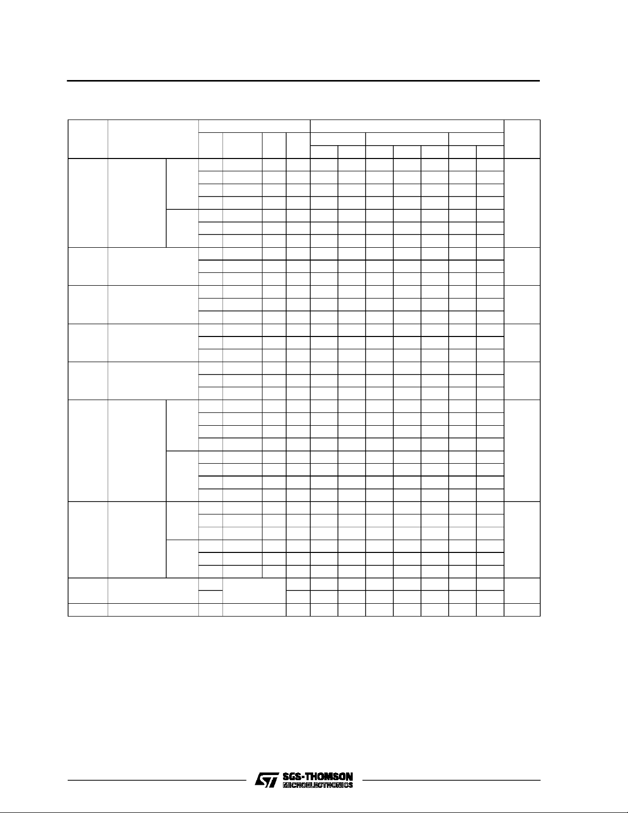
STATI C E LECT RIC AL CHAR ACTER I STI CS (over rec omm ended o pera t ing co nditions )
Test Conditios Value
Symbol Parameter
I
Quiescent
L
Current
HCC
Types
V
(V)
V
I
(V)
|IO|
(µA)
V
(V)
O
T
DD
*25
LOW
Min. Max. Min. Typ. Max. Min. Max.
0/5 5 1 0.02 1 30
0/10 10 2 0.02 2 60
0/15 15 4 0.02 4 120
o
CT
0/20 20 20 0.04 20 600
HCF
Types
0/5 5 4 0.02 4 30
0/10 10 8 0.02 8 60
0/15 15 16 0.02 16 120
OH
Output High
V
Voltage
0/5 < 1 5 4.95 4.95 4.95
0/10 < 1 10 9.95 9.95 9.95
0/15 < 1 15 14.95 14.95 14.95
V
OL
Output Low
Voltage
5/0 < 1 5 0.05 0.05 0.05
10/0 < 1 10 0.05 0.05 0.05
15/0 < 1 15 0.05 0.05 0.05
V
IH
Input High
Voltage
4.5 < 1 5 3.5 3.5 3.5
9<1107 7 7
13.5 < 1 15 11 11 11
V
IL
Input Low
Voltage
0.5 < 1 5 1.5 1.5 1.5
1<110 3 3 3
1.5 < 1 15 4 4 4
I
OH
Output
Drive
Current
HCC
Types
0/5 2.5 5 -2 -1.6 -3.2 -1.15
0/5 4.6 5 -0.64 -0.51 -1 -0.36
0/10 9.5 10 -1.6 -1.3 -2.6 -0.9
0/15 13.5 15 -4.2 -3.4 -6.8 -2.4
0/5 2.5 5 -1.53 -1.36 -3.2 -1.1
HCF
Types
0/5 4.6 5 -0.52 -0.44 -1 -0.36
0/10 9.5 10 -1.3 -1.1 -2.6 -0.9
0/15 13.5 15 -3.6 -3.0 -6.8 -2.4
I
OL
Output
Sink
Current
HCC
Types
HCF
Types
0/5 0.4 5 0.64 0.51 1 0.36
0/10 0.5 10 1.6 1.3 2.6 0.9
0/15 1.5 15 4.2 3.4 6.8 2.4
0/5 0.4 5 0.52 0.44 1 0.36
0/10 0.5 10 1.3 1.1 2.6 0.9
0/15 1.5 15 3.6 3.0 6.8 2.4
I
IH,IIL
C
*T
LOW
*T
HIGH
TheNoiseMargin for both”1” and”0” levelis: 1Vmin.withVDD=5V, 2V min.withVDD=10 V,2.5 Vmin. withVDD=15V
Input Leakage
Current
Input Capacitance Any Input 5 7.5 pF
I
=-55oCforHCCdevice: -40oC for HCF device.
=+125oCforHCC device: +85oC for HCF device.
0/18
0/15 15 ±0.3 ±10
Any Input
18 ±0.1 ±10-5±0.1 ±1
-5
±0.3 ±1
HIGH
Unit
*
µA
V
V
V
V
mA
mA
µA
4/13
 Loading...