

.CASCADABLEIN MULTIPLES OF 4-BITS
.SET TO ”15” INPUT AND ”15” DETECT OUT-
PUT
.QUIESCENT CURRENT SPECIFIED TO 20V
FOR HCC DEVICE
.STANDARDIZED SYMMETRICAL OUTPUT
CHARACTERISTICS
.INPUT CURRENT OF 100nA AT 18V AND
25°C FORHCC DEVICE
.100% TESTEDFOR QUIESCENTCURRENT
.MEETSALLREQUIREMENTSOFJEDECTEN-
TATIVE STANDARD No. 13A, ”STANDARD
SPECIFICATIONS FOR DESCRIPTIONOF ”B”
SERIESCMOS DEVICES”
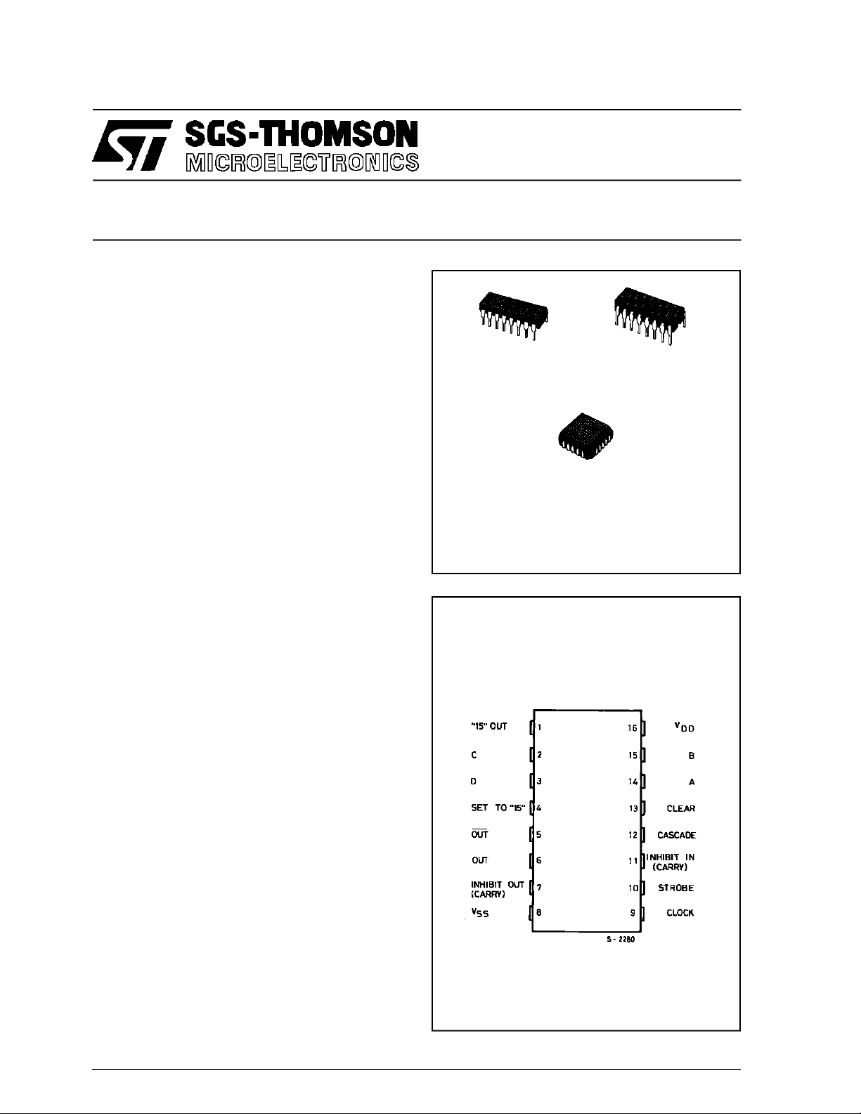
HCC/HCF4089B
BINARY RATE MULTIPLIER
EY
(Plastic Package)
C1
(ChipCarrier)
ORDERCODES :
HCC4089BF HCF4089BEY
(CeramicPackage)
HCF4089BC1
F
DESCRIPTION
TheHCC4089B(extended temperature range) and
HCF4089B (intermediate temperature range) are
monolithic integrated circuit available in 16-lead
dual in-line plastic or ceramic package.
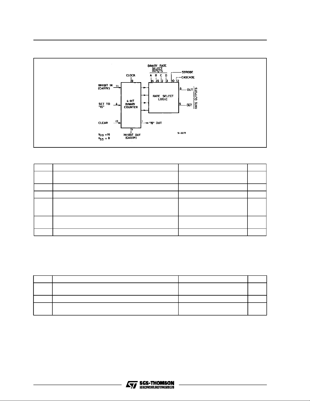
The HCC/HCF4089B is a low-power 4-bit digital
ratemultiplier thatprovides anoutput pulse ratethat
is the clock-input-pulse rate multiplied by1/16times
the binaryinput.For example,when thebinaryinput
numberis 13,therewillbe13outputpulsesforevery
16 input pulses.
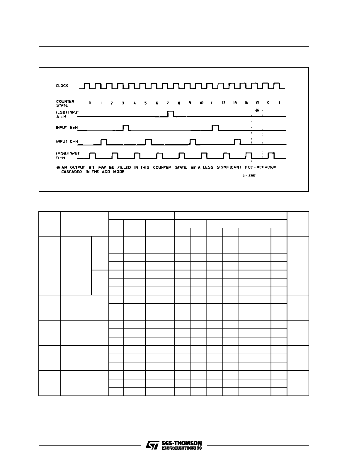
The HCC/HCF4089B has an internal synchronous
4-bit counter which,together with oneof the fourbinary input bits, produces pulse trains as shown in
timing diagram.
If morethanonebinaryinput bit ishigh, theresulting
pulse train is a combination of the above separate
pulse trains. This device may be used to perform
arithmetic operations (add, subtract, divide, raiseto
a power), solvealgebraic anddifferential equations,
generate natural logarithms and trigonometric functions, A/D and D/A conversions, and frequency division.
PIN CON NECT I ONS
June 1989
1/13
HCC/HCF4089B
FUNCTIONAL DIAGRAM
ABSOLUTE MAXIMU M RATINGS
Symbol Parameter Valu e Unit
V
* Supply Voltage :HCC Types
DD
HCF Types
V
Input Voltage – 0.5 to VDD+ 0.5 V
i
I
DC Input Current (any one input) ± 10 mA
I
P
Total Power Dissipation (per package)
tot
Dissipation per Output Transistor
for T
T
Operating Temperature : HCC Types
op
= Full Package-temperature Range
op
HCF Types
T
Stresses above those listed under ”Absolute Maximum Ratings” may cause permanent damage tothe device. This is a stress ratingonly and
functionaloperation of thedeviceatthese orany otherconditionsabove thoseindicatedintheoperationalsectionsofthisspecification isnotimplied.
Exposure to absolute maximum ratingconditionsfor externalperiodsmay affect device reliability.
*
Allvoltage valuesarereferredto VSSpinvoltage.
Storage Temperature – 65 to + 150 °C
stg
– 0.5 to + 20
– 0.5 to + 18
200
100
–55to+125
–40to+85
V
V
mW
mW
°C
°C
RECOMMENDED OPERATING CONDITIONS
Symbol Parameter Value Unit
V
T
2/13
Supply Voltage : HCC Types
DD
HCF Types
V
Input Voltage 0 to V
I
Operating Temperature : HCC Types
op
HCF Types
3to18
3to15
DD
– 55 t o + 125
–40to+85
V
V
V
°C
°C
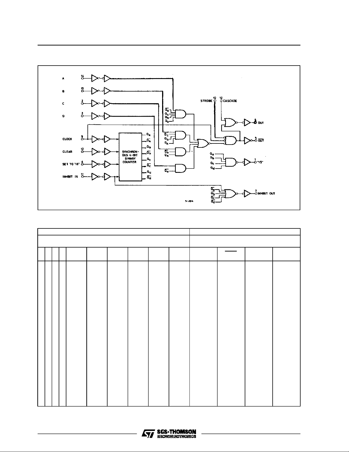
LOGIC DIAGRAM
HCC/HCF4089B
TRUTH TABLE
Number of Pulses o r I nput Logic Level
DCBA CLK
0
0
0
0
0
0
0
0
0
1
0
0
1
0
1
0
0
1
0
0
1
1
0
1
1
1
0
0
1
0
0
1
0
1
1
0
1
1
1
0
1
1
0
1
1
1
1
1
1
X
X
X
X
X
X
X
X
X
16
1
16
0
16
1
16
0
16
1
16
0
16
1
16
0
16
1
16
0
16
1
16
0
16
1
16
0
16
1
16
X
16
X
16
X
16
Inputs Outputs
(0= low;1 = high; X= don’tcare)
INH
IN
STR CAS CLR SET O U T OU T
0
0
0
0
0
0
0
0
0
0
0
0
0
0
0
0
1
0
0
0
0
0
0
0
0
0
0
0
0
0
0
0
0
0
0
0
1
0
0
0
0
0
0
0
0
0
0
0
0
0
0
0
0
0
0
0
1
Numbe r o f Pulses or Output Logic Level
0
0
0
0
0
0
0
0
0
0
0
0
0
0
0
0
0
0
0
0
0
0
0
0
0
0
0
0
0
0
0
0
0
0
0
0
0
0
L
1
2
3
4
5
6
7
8
9
10
11
12
13
14
15
•
L
H
(L= low; H = high)
INH
OUT
H
1
2
3
4
5
6
7
8
9
10
11
12
13
14
15
•
H
*
1
1
1
1
1
1
1
1
1
1
1
1
1
1
1
1
H
1
1
”15”
OUT
1
1
1
1
1
1
1
1
1
1
1
1
1
1
1
1
•
1
1
1
X
X
X
0
X
X
X
X
X
*
Output same as thefirst16 linesof thistruth table (depending on values of A,B,C,D).
16
X
16
X
16
0
0
0
0
0
0
0
0
0
1
1
0
0
0
1
• Depends on internalstateof counter.
16
L
L
16
H
H
H
H
L
L
L
H
3/13
HCC/HCF4089B
TIMING DIAGRAM
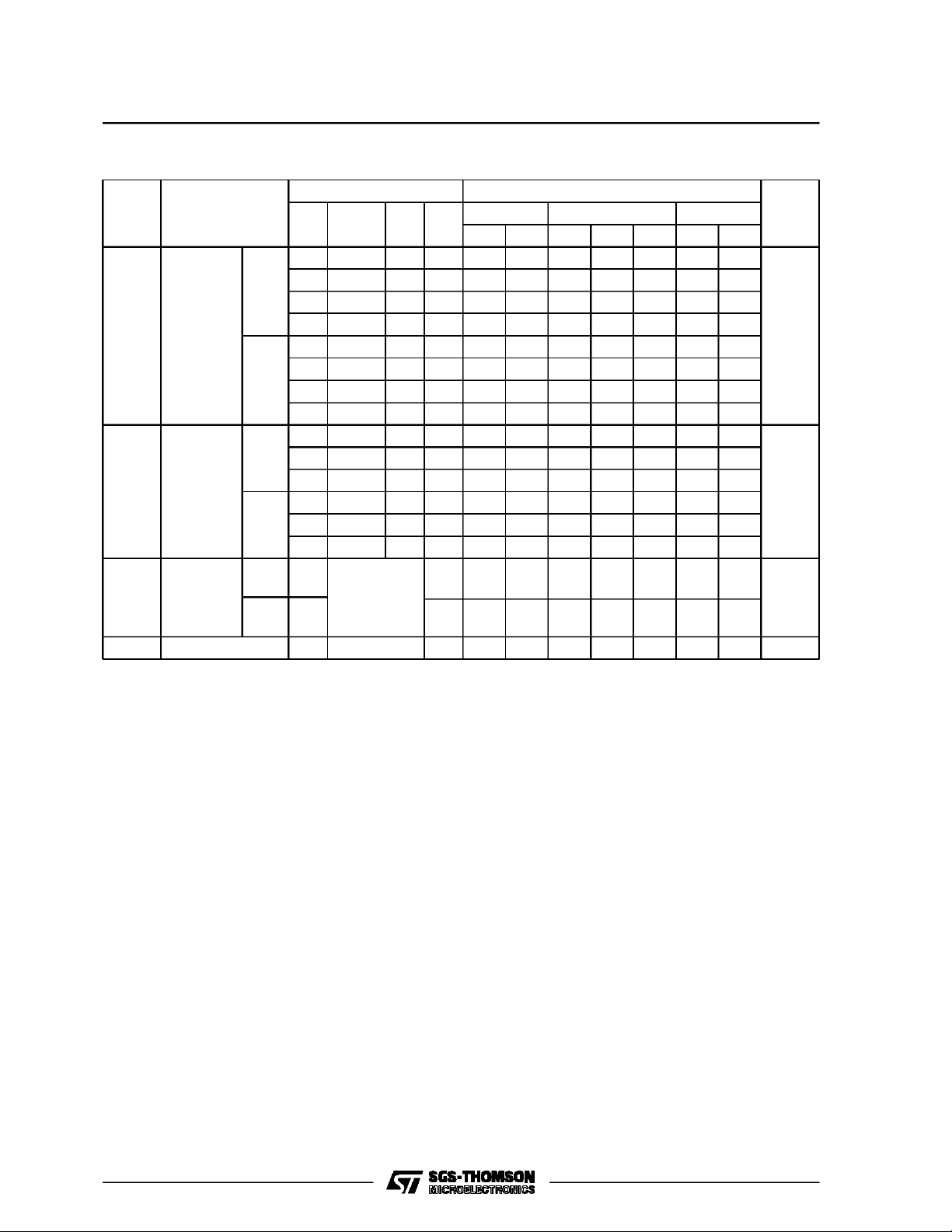
STATIC ELECTRICAL CHARACTERISTICS (over recommended operatingconditions)
Test Conditions Value
Symbol Parameter
I
Quiescent
L
Current
HCC
Types
V
V
I
O
|IO|V
(V) (V) (µA) (V)
0/ 5 5 5 0.04 5 150
0/10 10 10 0.04 10 300
0/15 15 20 0.04 20 600
T
* 25°CT
DD
Low
Min. Max. Min. Ty p. Max. Min. Max.
0/20 20 100 0.08 100 3000
0/ 5 5 20 0.04 20 150
HCF
Types
0/10 10 40 0.04 40 300
0/15 15 80 0.04 80 600
V
OH
Output High
Voltage
0/ 5 < 1 5 4.95 4.95 4.95
0/10 < 1 10 9.95 9.95 9.95
0/15 < 1 15 14.95 14.95 14.95
V
OL
Output Low
Voltage
5/0 < 1 5 0.05 0.05 0.05
10/0 < 1 10 0.05 0.05 0.05
15/0 < 1 15 0.05 0.05 0.05
V
IH
Input High
Voltage
0.5/4.5 < 1 5 3.5 3.5 3.5
1/9 < 1 10 7 7 7
1.5/13.5 < 1 15 11 11 11
V
IL
Input Low
Voltage
4.5/0.5 < 1 5 1.5 1.5 1.5
9/1 < 1 10 3 3 3
13.5/1.5 < 1 15 4 4
*T
=–55°CforHCC device: – 40°C for HCF device.
Low
*T
= +125°C forHCCdevice:+ 85°C for HCF device.
High
TheNoiseMarginfor both ”1” and ”0” levelis:1V min.with VDD=5V, 2V min. withVDD= 10V,2.5Vmin. withVDD= 15V.
High
Unit
*
µA
V
V
V
V
4/13
HCC/HCF4089B
STATIC ELECTRICAL CHARACTERISTICS (continued)
Test Conditions Value
Symbol Parameter
V
V
I
O
|IO|V
(V) (V) (µA) (V)
I
OH
Output
Drive
Current
HCC
Types
0/ 5 2.5 5 – 2 – 1.6 – 3.2 – 1.15
0/ 5 4.6 5 – 0.64 – 0.51 – 1 – 0.36
0/10 9.5 10 – 1.6 – 1.3 – 2.6 – 0.9
0/15 13.5 15 – 4.2 – 3.4 – 6.8 – 2.4
0/ 5 2.5 5 – 1.53 – 1.36 – 3.2 – 1.1
HCF
Types
0/ 5 4.6 5 – 0.52 – 0.44 – 1 – 0.36
0/10 9.5 10 – 1.3 – 1.1 – 2.6 – 0.9
0/15 13.5 15 – 3.6 – 3.0 – 6.8 – 2.4
I
OL
Output
Sink
Current
HCC
Types
0/ 5 0.4 5 0.64 0.51 1 0.36
0/10 0.5 10 1.6 1.3 2.6 0.9
0/15 1.5 15 4.2 3.4 6.8 2.4
0/ 5 0.4 5 0.52 0.44 1 0.36
HCF
Types
0/10 0.5 10 1.3 1.1 2.6 0.9
0/15 1.5 15 3.6 3.0 6.8 2.4
I
IH,IIL
*T
Low
*T
High
TheNoiseMarginfor both ”1” and ”0” levelis:1V min.with VDD=5V, 2V min. withVDD= 10V,2.5Vmin. withVDD= 15V.
Input
Leakage
Current
C
Input Capacitance Any Input 5 7.5 pF
I
=–55°CforHCC device: – 40°C for HCF device.
= +125°C forHCCdevice:+ 85°C for HCF device.
HCC
Types
HCF
Types
0/18
0/15
18 ± 0.1 ±10
Any Input
15 ± 0.3 ±10
T
* 25°CT
DD
Low
Min. Max. Min. Ty p. Max. Min. Max.
–5
± 0.1 ± 1
–5
± 0.3 ± 1
High
Unit
*
mA
mA
µA
5/13

HCC/HCF4089B
DYNAMIC ELECTRICAL CHARACTERISTICS (T
=25°C,CL= 50pF, RL= 200kΩ,
amb
typical temperature coefficient for all VDDvalues is 0.3%/°C, all input rise and fall times = 20ns)
Symbol Parameter
t
PHL,tPL H
Propagation
Clock to out 5 110 220
Delay Time
Clock or Strobe to
out
Clock to Inhibit
High Level to Low
Level
Low Level to High
Level
Clear to out 5 380 760
Clock to ”9” or
”15” out
Cascade to out 5 90 180
Inhibit in to Inhibit
out
Set to out 5 330 660
Test Conditions Value
(V) Min. Typ. M ax.
V
DD
10 55 110
15 45 90
5 150 300
10 75 150
15 60 120
5 360 720
10 160 320
15 110 220
5 250 500
10 100 200
15 75 150
10 175 350
15 130 260
5 300 600
10 125 250
15 90 180
10 45 90
15 35 70
5 160 320
10 75 150
15 55 110
10 150 300
15 110 220
Uni t
ns
ns
ns
ns
ns
ns
ns
ns
ns
6/13

DYNAMIC ELECTRICAL CHARACTERISTICS (continued )
HCC/HCF4089B
Symbol Parameter
t
THL,tTLH
f
CL
t
t
r,tf
t
W
t
se tu p
Transition Time 5 100 200
Maximum Clock Frequency 5 1.2 2.4
Clock Pulse Width 5 330 165
W
Clock Rise or Fall Time 5 15
Set or Clear Pulse Width 5 160 80
Inhibit Input Setup Time, High
Level to Low Level
t
t
t
Inhibit, Input Removal Time 5 240 120
R
Minimum Set Removal Time 5 150 75
R
Clear Removal Time 5 60 30
R
Test Conditions Value
V
(V) Min. Typ. M ax.
DD
10 50 100
15 40 80
10 2.5 5
15 3.5 7
10 170 85
15 100 50
10 15
15 15
10 90 45
15 60 30
5 100 50
10 40 20
15 20 10
10 130 65
15 110 55
10 80 40
15 50 25
10 40 20
15 30 15
Unit
ns
MHz
ns
µs
ns
ns
ns
ns
ns
7/13

HCC/HCF4089B
APPLICATION NOTES
Forwords of more than 4 bits, HCC/HCF4089B devices maybe cascaded in two different modes: anAdd
modeand a Multiply mode.
Two HCC/HCF4089B’s cascadedin the ”Add” mode with apreset number of 189.
Nota :
In theAdd mode some of the gaps left by the more
significant unit at the count of 15 are filledinby the
less significant units. For example, when two units
are cascaded inthe Add mode and programmed to
11 and13, respectively, themoresignificant unit will
have 11output pulsesfor every16 inputpulses and
the other unit will have 13 output pulses for every
256 input pulsesfor a totalof
11 13 189
+=
16 256 256
Two HCC/HCF4089B’scascaded in the Multiply mode for Multiplication of two variables AandB with loop
circuitcontrol.
When the loopstabilies rate R2 = rateR3, thus fclock( . ) = fclock ( . ) therefore N = A.B
8/13
AB 1N
16 16 16 16
.

TEST CIRCUITS
HCC/HCF4089B
QuiescentDeviceCurrent.
Input Leakage Current.
Noise Immunity.
9/13

HCC/HCF4089B
Plastic DIP16 (0.25) MECHANICAL DATA
DIM.
MIN. TYP. MAX. MIN. TYP. MAX.
a1 0.51 0.020
B 0.77 1.65 0.030 0.065
b 0.5 0.020
b1 0.25 0.010
D 20 0.787
E 8.5 0.335
e 2.54 0.100
e3 17.78 0.700
F 7.1 0.280
I 5.1 0.201
L 3.3 0.130
Z 1.27 0.050
mm inch
10/13
P001C

Ceramic DIP16/1 MECHANICAL DATA
HCC/HCF4089B
DIM.
MIN. TYP. MAX. MIN. TYP. MAX.
A 20 0.787
B 7 0.276
D 3.3 0.130
E 0.38 0.015
e3 17.78 0.700
F 2.29 2.79 0.090 0.110
G 0.4 0.55 0.016 0.022
H 1.17 1.52 0.046 0.060
L 0.22 0.31 0.009 0.012
M 0.51 1.27 0.020 0.050
N 10.3 0.406
P 7.8 8.05 0.307 0.317
Q 5.08 0.200
mm inch
P053D
11/13

HCC/HCF4089B
PLCC20 MECHANICAL DATA
DIM.
MIN. TYP. MAX. MIN. TYP. MAX.
A 9.78 10.03 0.385 0.395
B 8.89 9.04 0.350 0.356
D 4.2 4.57 0.165 0.180
d1 2.54 0.100
d2 0.56 0.022
E 7.37 8.38 0.290 0.330
e 1.27 0.050
e3 5.08 0.200
F 0.38 0.015
G 0.101 0.004
M 1.27 0.050
M1 1.14 0.045
mm inch
12/13
P027A

HCC/HCF4089B
Information furnished is believed tobe accurate and reliable. However, SGS-THOMSON Microelectronicsassumes no responsability for the
consequences of use of such information nor for any infringementofpatents orother rights of third parties which may results from its use. No
license isgrantedby implication orotherwiseunder any patentorpatent rights of SGS-THOMSONMicroelectronics.Specificationsmentioned
in this publication are subject to changewithout notice.Thispublication supersedes andreplacesallinformationpreviouslysupplied.
SGS-THOMSON Microelectronicsproductsare notauthorizedforuse ascriticalcomponentsinlife supportdevicesor systemswithout express
written approval of SGS-THOMSON Microelectonics.
1994 SGS-THOMSON Microelectronics - All RightsReserved
Australia - Brazil - France - Germany - Hong Kong - Italy - Japan - Korea - Malaysia - Malta - Morocco - The Netherlands-
Singapore - Spain - Sweden - Switzerland - Taiwan - Thailand - UnitedKingdom - U.S.A
SGS-THOMSON MicroelectronicsGROUPOF COMPANIES
13/13
 Loading...