

4071B - QUAD 2–INPUT OR GATE
4072B - QUAD 4–INPUT OR GATE
4075B - TRIPLE 3–INPUT OR GATE
HCC4071B/72B/75B
HCF4071B/72B/75B
OR GATE
.MEDIUM-SPEED OPERATION t
60ns. (typ.) AT VDD= 10V
PLH
,t
PHL
.QUIESCENT CURRENT SPECIFIED TO 20V
FOR HCC DEVICE
.5V, 10V AND 15V PARAMETRIC RATINGS
.INPUT CURRENT OF 100nA AT 18V AND
25°C FORHCC DEVICE
.100% TESTEDFOR QUIESCENTCURRENT
.MEETSALLREQUIREMENTSOFJEDECTEN-
TATIVE STANDARD No. 13A, ”STANDARD
SPECIFICATIONS FOR DESCRIPTIONOF ”B”
SERIESCMOS DEVICES”
DESCRIPTION
TheHCC4071B/4072B and4075B (extended tem-
peraturerange)andHCF4071B/4072B and 4075B
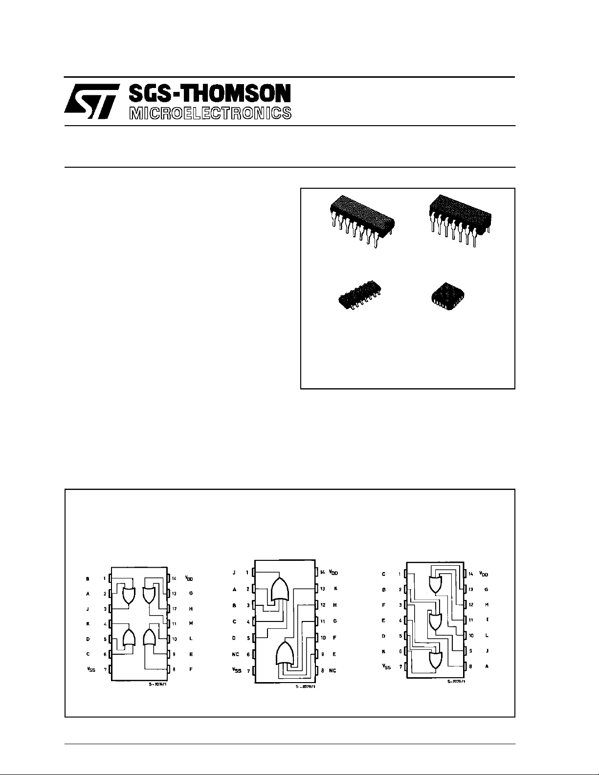
(intermediate temperature range)are monolithic integrated circuits, available in 14-lead dual in-line
plastic or ceramic package and plastic micropackage.
PIN CONNECTIONS
4071B 4072B 4075B
=
EY
(Plastic Package)F(Ceramic Frit SealPackage)
M1
(MicroPackage)
ORDER CODES :
HCC40XXBF HCF40XXBM1
HCF40XXBEY HCF40XXBC1
TheHCC/HCF4071B,4072B and 4075B OR gates
provide the system designer with direct implementation of the positive-logic OR functionand supplement theexisting family of COS/MOSgates.
(PlasticChipCarrier)
C1
June1989
1/11
HCC/H FC4071B/72B/75B
ABSOLUTE MAXI MUM RATI N GS
Symbol Parameter Value Unit
V
* Supply Voltage : HCC Types
DD
HCF Types
V
Input Voltage – 0.5 to VDD+ 0.5 V
i
I
DC Input Current (any one input) ± 10 mA
I
P
Total Power Dissipation (per package)
tot
Dissipation per Output Transistor
for Top = Full Package-temperature Range
T
Operating Temperature : HCC Types
op
HCF Types
T
Stresses above those listed under ”Absolute Maximum Ratings” may cause permanent damage to the device. This is a stress
rating only and functional operation of the device at these or any other conditions above those indicated in the operational sections of this specification is not implied. Exposure to absolute maximum rating conditions for external periods may affect device
reliability.
* Allvoltage values arereferred to VSSpinvoltage.
Storage Temperature – 65 to + 150 °C
stg
RECOMMENDED OPERATING CONDITIONS
Symbol Parameter Value Unit
V
T
Supply Voltage : HCC Types
DD
HCF Types
V
Input Voltage 0 to V
I
Operating Temperature : HCC Types
op
HCF Types
– 0.5 to + 20
– 0.5 to + 18
200
100
– 55 to + 125
–40to+85
3to18
3to15
DD
– 55 to + 125
–40to+85
V
V
mW
mW
°C
°C
V
V
V
°C
°C
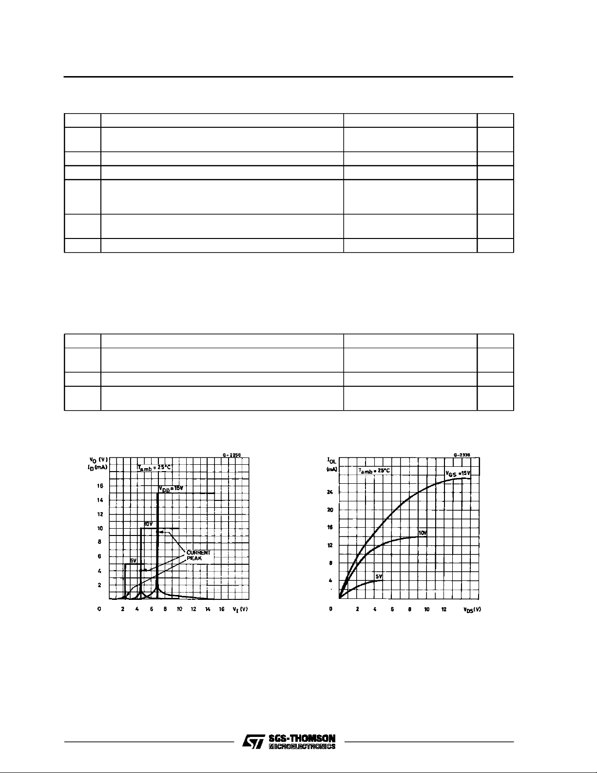
TypicalVoltage and Current Transfer
Characteristics.
TypicalOutput Low (sink) Current Characterisitcs.
2/11
HCC/HCF4071B/72B/75B
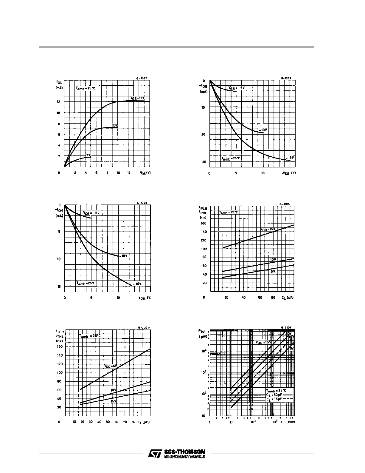
Minimum Output Low (sink) Current Characteristics.
Minimum Output High(source)Current Characterisitcs.
TypicalOutput High (source) Current Characteristics.
TypicalPropagation Delay Time vs. Load Capacitance.
TypicalTransition Time vs. Load Capacitance. TypicalDynamic Power Dissipation vs.Fre-
quency.
3/11
HCC/H FC4071B/72B/75B
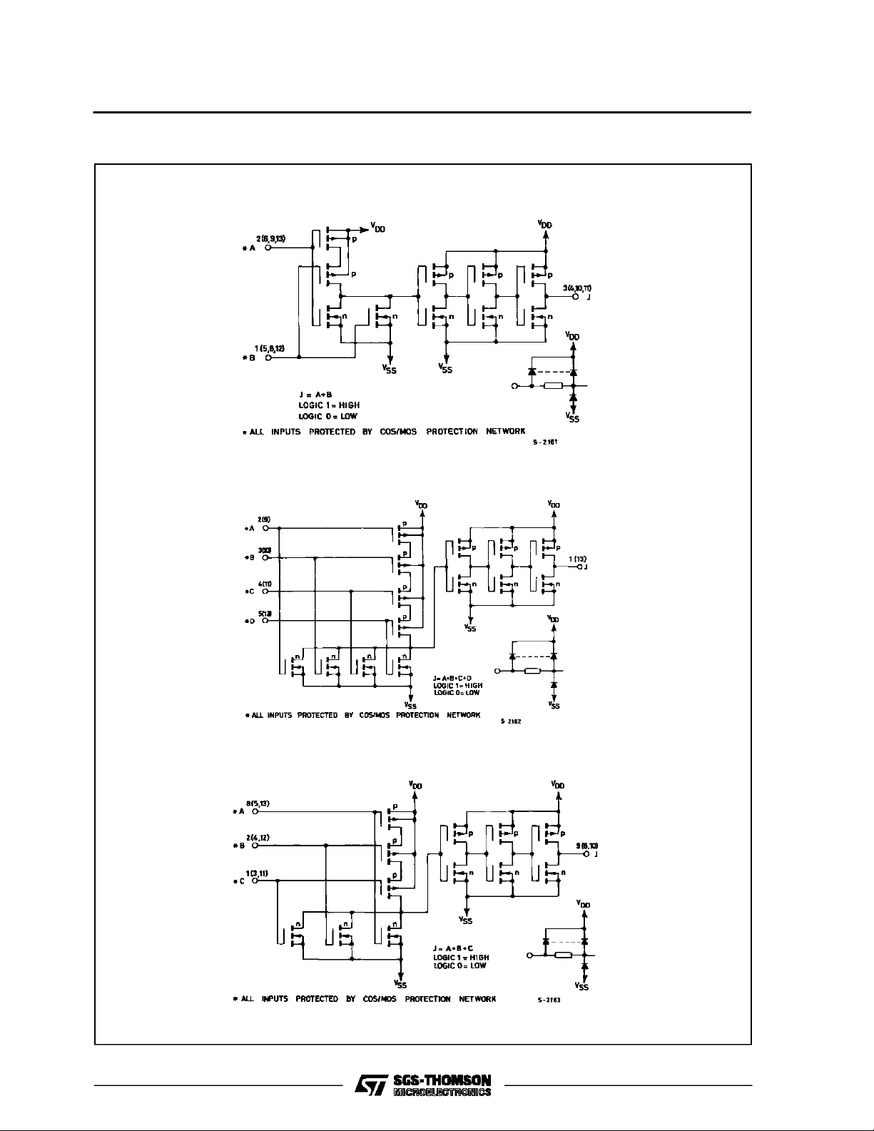
SCHEMATIC DIAGRAMS
4071B – 1 of4 identical OR gates
4072B – 1 of 2 identical OR gates
4075B – 1 of 3 identical OR gates
4/11

HCC/HCF4071B/72B/75B
STATIC ELECTRICAL CHARACTERISTICS (over recommended operating conditions)
Test Conditions Value
Symbol Parameter
(V) (V) (µA) (V)
I
L
Quiescent
Current
HCC
Types
0/ 5 5 0.25 0.01 0.25 7.5
0/10 10 0.5 0.01 0.5 15
0/15 15 1 0.01 1 30
0/20 20 5 0.02 5 150
0/ 5 5 1 0.01 1 7.5
HCF
Types
0/10 10 2 0.01 2 15
0/15 15 4 0.01 4 30
V
OH
Output High
Voltage
0/ 5 < 1 5 4.95 4.95 4.95
0/10 < 1 10 9.95 9.95 9.95
0/15 < 1 15 14.95 14.95 14.95
V
OL
Output Low
Voltage
5/0 < 1 5 0.05 0.05 0.05
10/0 < 1 10 0.05 0.05 0.05
15/0 < 1 15 0.05 0.05 0.05
V
IH
Input High
Voltage
V
IL
Input Low
Voltage
I
OH
Output
Drive
Current
HCC
Types
0/ 5 2.5 5 – 2 – 1.6 – 3.2 – 1.15
0/ 5 4.6 5 – 0.64 – 0.51 – 1 – 0.36
0/10 9.5 10 – 1.6 – 1.3 – 2.6 – 0.9
0/15 13.5 15 – 4.2 – 3.4 – 6.8 – 2.4
0/ 5 2.5 5 – 1.53 – 1.36 – 3.2 – 1.1
HCF
Types
0/ 5 4.6 5 – 0.52 – 0.44 – 1 – 0.36
0/10 9.5 10 – 1.3 – 1.1 – 2.6 – 0.9
0/15 13.5 15 – 3.6 – 3.0 – 6.8 – 2.4
I
OL
Output
Sink
Current
HCC
Types
0/ 5 0.4 5 0.64 0.51 1 0.36
0/10 0.5 10 1.6 1.3 2.6 0.9
0/15 1.5 15 4.2 3.4 6.8 2.4
0/ 5 0.4 5 0.52 0.44 1 0.36
HCF
Types
0/10 0.5 10 1.3 1.1 2.6 0.9
0/15 1.5 15 3.6 3.0 6.8 2.4
I
IH,IIL
*T
*T
TheNoiseMarginfor both ”1” and ”0” levelis:1V min.with VDD=5V,2V min. withVDD= 10V,2.5V min.with VDD= 15V.
Input
Leakage
Current
C
Input Capacitance Any Input 5 7.5 pF
I
=–55°CforHCC device : – 40°C for HCF device.
Low
= + 125°CforHCC device : + 85°CforHCF device.
High
HCC
Types
HCF
Types
0/18
0/15
V
V
I
O
|IO|V
DD
T
* 25°CT
Low
Min. M ax. Min. Typ. Max. Min. Max.
0.5/4.5 < 1 5 3.5 3.5 3.5
1/9 < 1 10 7 7 7
1.5/13.5 < 1 15 11 11 11
4.5/0.5 < 1 5 1.5 1.5 1.5
9/1 < 1 10 3 3 3
13.5/1.5 < 1 15 4 4 4
–5
18 ± 0.1 ±10
± 0.1 ± 1
Any Input
15 ± 0.3 ±10
–5
± 0.3 ± 1
High
Unit
*
µA
V
V
V
V
mA
mA
µA
5/11

HCC/H FC4071B/72B/75B
DYNAMIC ELECTRICAL CHARACTERISTICS (T
=25°C, CL= 50pF, RL= 200kΩ,
amb
typical temperature coefficient for all VDD= 0.3%/°C values , all input rise and fall time = 20ns)
Symbol Parameter
t
PHL
t
PLH
t
THL,tTLH
Propagation Delay Time 5 125 250
Propagation Delay Time 5 175 350
Transition Time 5 100 200
Test Conditions
V
(V) Min. Typ. Max.
DD
10 60 120
15 45 90
70 50 140
15 50 140
10 50 100
15 40 80
Value
TEST CIRCUITS
QuiescentDeviceCurrent. Input Voltage.
Unit
ns
ns
ns
Input Leakage Current.
6/11

HCC/HCF4071B/72B/75B
Plastic DIP14 MECHANICAL DATA
DIM.
MIN. TYP. MAX. MIN. TYP. MAX.
a1 0.51 0.020
B 1.39 1.65 0.055 0.065
b 0.5 0.020
b1 0.25 0.010
D 20 0.787
E 8.5 0.335
e 2.54 0.100
e3 15.24 0.600
F 7.1 0.280
I 5.1 0.201
L 3.3 0.130
Z 1.27 2.54 0.050 0.100
mm inch
P001A
7/11

HCC/H FC4071B/72B/75B
Ceramic DIP14/1 MECHANICAL DATA
DIM.
MIN. TYP. MAX. MIN. TYP. MAX.
A 20 0.787
B 7.0 0.276
D 3.3 0.130
E 0.38 0.015
e3 15.24 0.600
F 2.29 2.79 0.090 0.110
G 0.4 0.55 0.016 0.022
H 1.17 1.52 0.046 0.060
L 0.22 0.31 0.009 0.012
M 1.52 2.54 0.060 0.100
N 10.3 0.406
P 7.8 8.05 0.307 0.317
Q 5.08 0.200
mm inch
8/11
P053C

SO14 MECHANICAL DATA
HCC/HCF4071B/72B/75B
DIM.
MIN. TYP. MAX. MIN. TYP. MAX.
A 1.75 0.068
a1 0.1 0.2 0.003 0.007
a2 1.65 0.064
b 0.35 0.46 0.013 0.018
b1 0.19 0.25 0.007 0.010
C 0.5 0.019
c1 45° (typ.)
D 8.55 8.75 0.336 0.344
E 5.8 6.2 0.228 0.244
e 1.27 0.050
e3 7.62 0.300
F 3.8 4.0 0.149 0.157
G 4.6 5.3 0.181 0.208
L 0.5 1.27 0.019 0.050
M 0.68 0.026
S8°(max.)
mm inch
P013G
9/11

HCC/H FC4071B/72B/75B
PLCC20 MECHANICAL DATA
DIM.
MIN. TYP. MAX. MIN. TYP. MAX.
A 9.78 10.03 0.385 0.395
B 8.89 9.04 0.350 0.356
D 4.2 4.57 0.165 0.180
d1 2.54 0.100
d2 0.56 0.022
E 7.37 8.38 0.290 0.330
e 1.27 0.050
e3 5.08 0.200
F 0.38 0.015
G 0.101 0.004
M 1.27 0.050
M1 1.14 0.045
mm inch
10/11
P027A

HCC/HCF4071B/72B/75B
Information furnished is believed to be accurate and reliable. However, SGS-THOMSON Microelectronics assumes no responsability for the
consequences of use of such information nor for any infringementofpatents orother rights of third parties which may results from its use. No
license isgrantedby implication or otherwiseunder any patent orpatentrights of SGS-THOMSONMicroelectronics.Specificationsmentioned
in this publication are subject to changewithout notice. This publication supersedes andreplaces all information previously supplied.
SGS-THOMSON Microelectronicsproductsare notauthorizedforuseascritical componentsin life supportdevices orsystemswithout express
written approval of SGS-THOMSON Microelectonics.
1994 SGS-THOMSON Microelectronics - All RightsReserved
Australia - Brazil - France - Germany - Hong Kong - Italy - Japan - Korea - Malaysia - Malta - Morocco - The Netherlands -
Singapore - Spain - Sweden - Switzerland - Taiwan - Thailand - UnitedKingdom - U.S.A
SGS-THOMSON MicroelectronicsGROUPOF COMPANIES
11/11
 Loading...