

SGS Thomson Microelectronics HCF4069UBM1, HCF4069UBEY, HCF4069UBC1, HCC4069UBF Datasheet
. MEDIUM-SPEED OPERATION
–t
PHL,tPLH
= 30ns(typ.)AT 10V
.QUIESCENT CURRENT SPECIFIED TO 20V
FOR HCC DEVICE
.STANDARDIZED SYMMETRICAL OUTPUT
CHARACTERISTICS
.5V, 10V,AND 15V PARAMETRIC RATINGS
.INPUT CURRENT OF 100nA AT 18V AND
25°C FORHCC DEVICE
.100% TESTEDFOR QUIESCENTCURRENT
.MEETSALLREQUIREMENTSOFJEDECTEN-
TATIVESTANDARDN°13A,”STANDARDSPECIFICATIONS FOR DESCRIPTION OF ”B”
SERIESCMOS DEVICES”
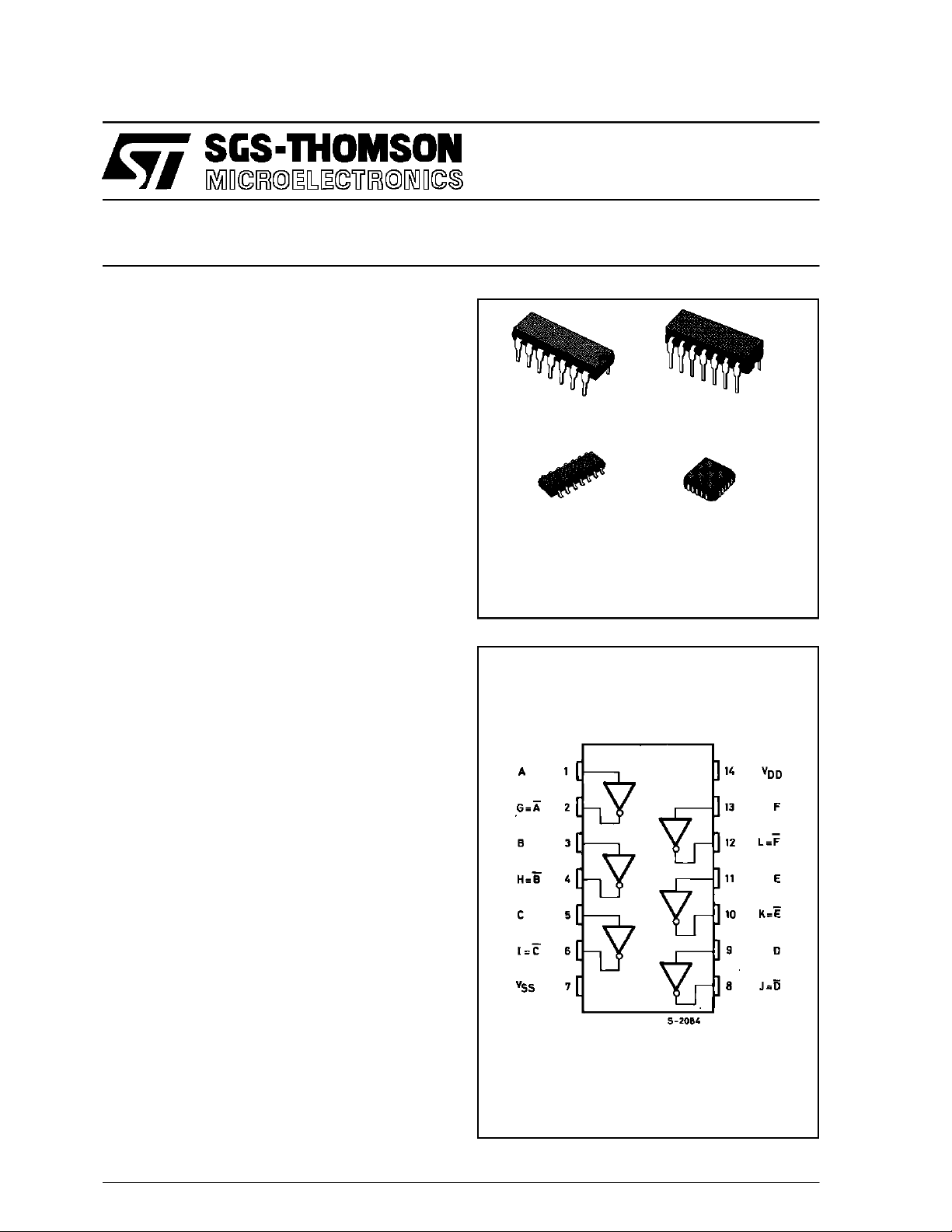
HCC/HCF4069UB
HEX INVERTER
EY
(Plastic Package)F(Ceramic FritSeal Package)
M1
(MicroPackage)
ORDER CODES :
HCC4069UBF HCF4069UBM1
HCF4069UBEY HCF4069UBC1
(PlasticChipCarrier)
C1
DESCRIPT ION
The HCC4069UB (extended temperature range)
andHCF4069UB(intermediatetemperature range)
aremonolithicintegratedcircuit, availablein14-lead
dual in-line plastic or ceramic package and plastic
micro package.
TheHCC/HCF4069UBconsistsofsixCOS/MOSinvertercircuits.Thisdeviceis intended forall generalpurpose inverter applications where the
medium-power TTL-drive and logic-level-conversioncapabilities ofcircuits suchasHCC/HCF4049B
Hex Inverter/Buffers arenot required.
PIN CONNECTIONS
June1989
1/12
HCC/HCF4069UB
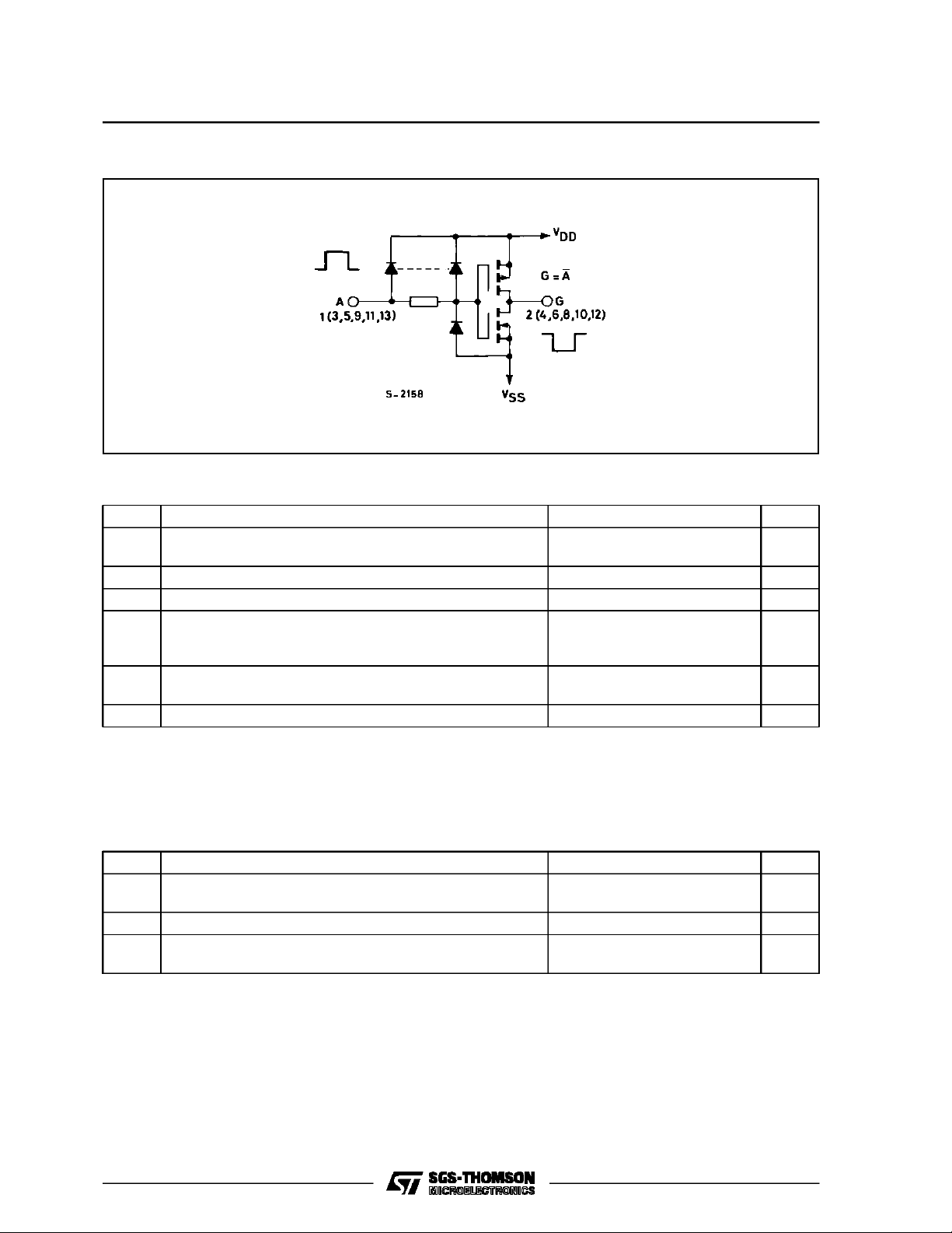
SCHEMATIC DIAGRAM O F ONE OF SIX IDENTICAL IN VERTERS.
ABSOLUTE M AXI MUM RATING S
Symbol Parameter Value Unit
V
* Supply Voltage : HCC Types
DD
HCF Types
V
Input Voltage – 0.5 to VDD+ 0.5 V
i
I
DC Input Current (any one input) ± 10 mA
I
P
Total Power Dissipation (per package)
tot
Dissipation per Output Transistor
for Top = Full Package-temperature Range
T
Operating Temperature : HCC Types
op
HCF Types
T
Stresses above those listed under ”Absolute Maximum Ratings” may cause permanent damage to the device. This is a stress
rating only and functional operation of the device at these or any other conditions above those indicated in the operational sections of this specification is not implied. Exposure to absolute maximum rating conditions for external periods may affect device
reliability.
* All voltage values are referred to VSSpin voltage.
Storage Temperature – 65 to + 150 °C
stg
– 0.5 to + 20
– 0.5 to + 18
200
100
– 55 to + 125
–40to+85
V
V
mW
mW
°C
°C
RECOMMENDED OPERATING CO NDITIONS
Symbol Parameter Value Unit
2/12
V
Supply Voltage : HCC Types
DD
HCF Types
V
Input Voltage 0 to V
I
T
Operating Temperature : HCC Types
op
HCF Types
3to18
3to15
DD
– 55 to + 125
–40to+85
V
V
V
°C
°C
HCC/HCF4069UB
STATIC ELECTRICAL CHARACTERISTICS (over recommended operating conditions)
Test Conditions Value
Symbol Parameter
I
Quiescent
L
Current
HCC
Types
HCF
Types
V
OH
Output High
Voltage
V
OL
Output Low
Voltage
V
IH
Input High
Voltage
IL
Input Low
V
Voltage
I
OH
Output
Drive
Current
HCC
Types
HCF
Types
I
OL
Output
Sink
Current
HCC
Types
HCF
Types
I
IH,IIL
Input
Leakage
Current
HCC
Types
HCF
Types
Input Capacitance Any Input 5 7.5 pF
C
I
*T
=–55°CforHCC device : – 40°CforHCF device.
Low
*T
= + 125°CforHCC device : + 85°CforHCF device.
High
The Noise Margin for both ”1” and ”0” level is : 1V min. with VDD= 5V, 2V min. with VDD= 10V, 2.5V min. with VDD= 15V.
V
V
O
|IO|V
I
(V) (V) (µA) (V)
T
DD
* 25°CT
Low
Min. Max. Min. Ty p. Max. Min. Max .
High
*
0/ 5 5 0.25 0.01 0.25 7.5
0/10 10 0.5 0.01 0.5 15
0/15 15 1 0.01 1 30
0/20 20 5 0.02 5 150
0/ 5 5 1 0.01 1 7.5
0/10 10 2 0.01 2 15
0/15 15 4 0.01 4 30
0/ 5 < 1 5 4.95 4.95 4.95
0/10 < 1 10 9.95 9.95 9.95
0/15 < 1 15 14.95 14.95 14.95
5/0 < 1 5 0.05 0.05 0.05
10/0 < 1 10 0.05 0.05 0.05
15/0 < 1 15 0.05 0.05 0.05
0.5/4.5 < 1 5 4 4 4
1/9 < 1 10 8 8 8
1.5/13.5 < 1 15 12.5 12.5 12.5
4.5/0.5 < 1 5 1 1 1
9/1 < 1 10 2 2 2
13.5/1.5 < 1 15 2.5 2.5 2.5
0/ 5 2.5 5 – 2 – 1.6 – 3.2 – 1.15
0/ 5 4.6 5 – 0.64 – 0.51 – 1 – 0.36
0/10 9.5 10 – 1.6 – 1.3 – 2.6 – 0.9
0/15 13.5 15 – 4.2 – 3.4 – 6.8 – 2.4
0/ 5 2.5 5 – 1.53 – 1.36 – 3.2 – 1.1
0/ 5 4.6 5 – 0.52 – 0.44 – 1 – 0.36
0/10 9.5 10 – 1.3 – 1.1 – 2.6 – 0.9
0/15 13.5 15 – 3.6 – 3.0 – 6.8 – 2.4
0/ 5 0.4 5 0.64 0.51 1 0.36
0/10 0.5 10 1.6 1.3 2.6 0.9
0/15 1.5 15 4.2 3.4 6.8 2.4
0/ 5 0.4 5 0.52 0.44 1 0.36
0/10 0.5 10 1.3 1.1 2.6 0.9
0/15 1.5 15 3.6 3.0 6.8 2.4
0/18
18 ± 0.1 ±10
–5
± 0.1 ± 1
Any Input
0/15
15 ± 0.3 ±10
–5
± 0.3 ± 1
Unit
µA
V
V
V
V
mA
mA
µA
3/12
HCC/HCF4069UB
DYNAMIC ELECTRICAL CHARACTERISTICS (T
=25°C, CL= 50pF, RL= 200kΩ,
amb
typical temperature coefficientfor all VDD= 0.3%/°C values,all input rise and fall time = 20ns)
Symbol Parameter
t
PLH,tPHL
t
TL H,tTHL
Propagation Delay Time 5 55 110
Transition Time 5 100 200
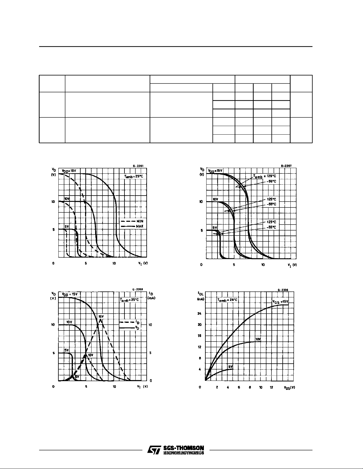
Minimum and Maximum Voltage TransferCharacteristics.
Test Conditions
(V) Min. Typ. Ma x.
V
DD
10 30 60
15 25 50
10 50 100
15 40 80
TypicalVoltage Transfer Characteristics asa
Function of Temperature.
Value
Unit
ns
ns
TypicalCurrent and Voltage Transfer Characteristics.
4/12
Typical OutputLow (sink)Current Characteristics.
 Loading...