

HIGH VOLTAGE FAST-SWITCHING
■ SGS-THOMSONPREFERRED SALESTYPE
■ HIGH VOLTAGECAPABILITY
■ VERYHIGH SWITCHINGSPEED
■ MINIMUMLOT-TO-LOT SPREADFOR
RELIABLEOPERATION
■ LOW BASE-DRIVEREQUIREMENTS
APPLICATIONS:
■ SWITCHMODE POWER SUPPLIES
■ MOTORCONTROL
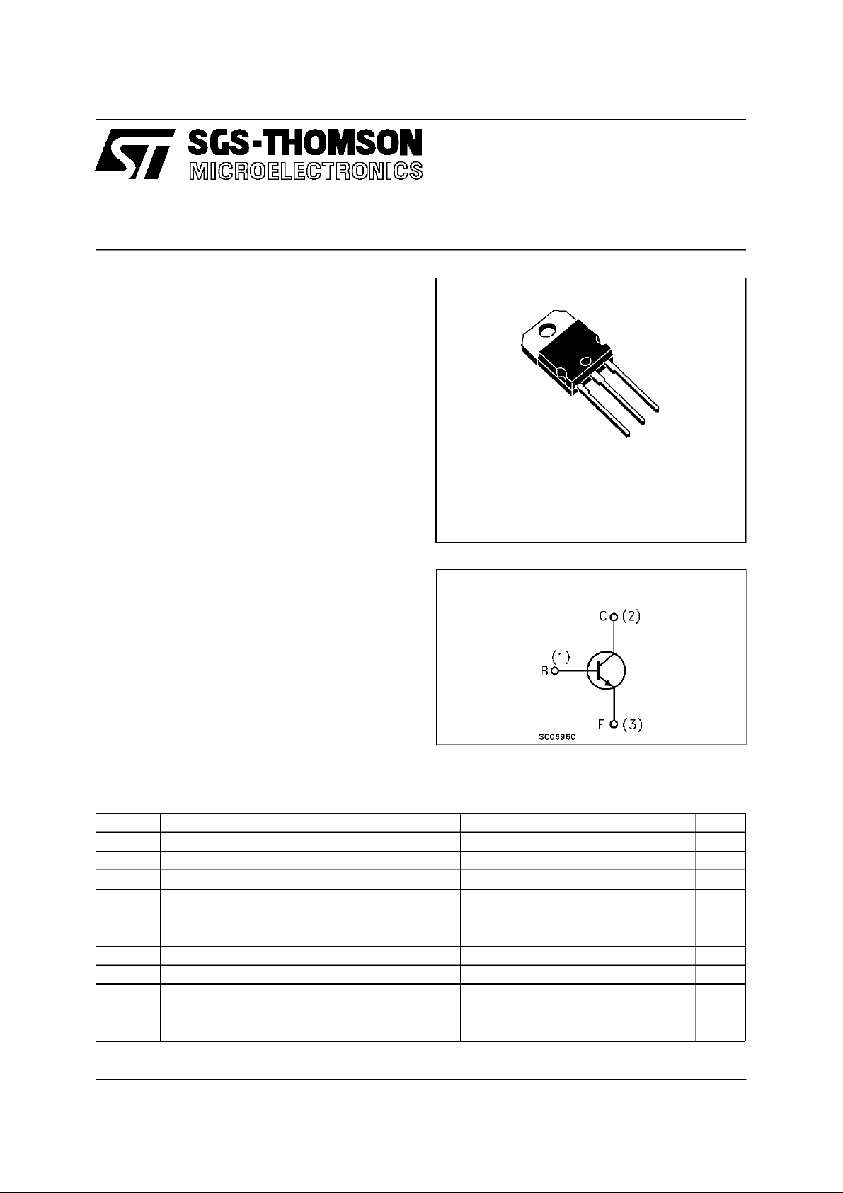
BUF410
NPN POWER TRANSISTOR
3
2
1
DESCRIPTION
The BUF410 is manufactured using High Voltage
TO-218
Multi Epitaxial Planar technology for high
switchingspeeds and high voltagecapacity. They
use a Cellular Emitter structure with planar edge
termination to enhance switching speeds while
maintaininga wide RBSOA.
The BUF series is designed for use in
INTERNAL SCHEMATIC DIAGRAM
high-frequency power supplies and motor control
applications.
ABSOLUTE MAXIMUM RATINGS
Symb o l Parameter Value Uni t
V
V
V
I
I
P
T
Collector-Emitte r Voltage ( VBE= -1. 5 V) 850 V
CEV
Collector-Emitte r Voltage ( IB= 0) 450 V
CEO
Emit t er-Base Volt age ( IC=0) 7 V
EBO
Collector Current 15 A
I
C
Collector P e ak Current (tp<5ms) 30 A
CM
Base Current 3 A
I
B
Base Pe ak C urr ent ( tp<5ms) 4.5 A
BM
Total Dissipation at Tc=25oC 125 W
tot
St orage T emperature -65 to 15 0
stg
Max O per ation Junc t ion T emperature 150
T
j
Max. Op erating J un c tion Temperature 150
T
j
o
C
o
C
o
C
July 1997
1/6

BUF410
THERMAL DATA
R
thj-case
Ther mal Resistance Junc t io n-Cas e M ax 1
o
C/W
ELECTRICAL CHARACTERISTICS (T
=25oC unless otherwise specified)
case
Symbol Parameter Test Cond ition s Min. Typ. Max. Unit
I
CER
I
CEV
I
EBO
V
CEO(sus )
Collector C ut -off
Current (R
=100Ω)
BE
Collector C ut -off
Current (I
B
=0)
Emit ter Cut - o f f C urr ent
(I
=0)
C
∗ Collec tor-Emit ter
V
CE=VCEV
VCE=V
V
V
V
CEVTc
CE=VCEVVBE
CE=VCEVVBE
=5V 1 mA
BE
=100oC
=-1.5V
= -1.5 V Tc=100oC
0.2
1
0.2
1
IC= 200 mA L = 25 mH 450 V
Sust aining V olt ag e
V
V
CE(sat)
EBO
Emit ter B ase Voltage
=0)
(I
C
∗ Collector-Emit t er
Saturation Voltage
V
∗ Base-Emitt er
BE(sat)
Saturation Voltage
di
/dt Rate of rise on-state
c
Collector C ur rent
V
(3µs) Collect or-E mitter
CE
Dynamic Volt age
V
(5µs) Collect or-E mitter
CE
Dynamic Volt age
t
t
St orage Time
s
Fall T ime
t
f
Cross Over Time
c
I
=50mA 7 V
E
IC=5A IB= 0.5 A
=5A IB=0.5A Tc=100oC
I
C
I
=10 A IB=2A
C
=10 A IB=2A Tc=100oC
I
C
IC=5A IB= 0.5 A
=5A IB=0.5A Tc=100oC
I
C
=10 A IB=2A
I
C
=10 A IB=2A Tc=100oC
I
C
0.8
2.8
0.5
2
0.9
1.5
1.1
1.5
VCC=300V RC=0 tp=3µs
=0.75A Tj=25oC
I
B1
=0.75A Tj=100oC
I
B1
=3A Tj=100oC
I
B1
45
100
60 A/µs
VCC=300V RC=60Ω
=0.75A Tj=25oC
I
B1
I
=0.75A Tj=100oC
B1
2.1
8
VCC=300V RC=60Ω
=0.75A Tj=25oC
I
B1
=0.75A Tj=100oC
I
B1
IC=5A VCC=50V
V
=-5V RBB=1.2 Ω
BB
= 400 V IB1=0.5A
V
clamp
1.1
4
0.8
0.05
0.08
L=0.5mH
1.8
0.1
0.18
V
t
s
t
f
t
c
CEW
t
s
t
f
t
c
St orage Time
Fall T ime
Cross Over Time
Maximum Collector
Emit ter V oltage
without Snubber
St orage Time
Fall T ime
Cross Over Time
IC=5A VCC=50V
=-5V RBB=1.2 Ω
V
BB
= 400 V IB1=0.5A
V
clamp
L=0.5mH T
=100oC
j
IC=5A VCC=50V
=-5V RBB=1.2 Ω
V
BB
= 400 V IB1=0.5A
V
clamp
L=0.5mH T
=125oC
j
IC=5A VCC=50V
=0 RBB=0.3Ω
V
BB
= 400 V IB1=0.5A
V
clamp
500 V
1.5
0.04
0.07
L=0.5mH
mA
mA
mA
mA
V
V
V
V
V
V
V
V
A/µs
A/µs
V
V
V
V
µs
µs
µs
µs
µs
µs
µs
µs
µs
2/6

BUF410
ELECTRICAL CHARACTERISTICS (continued)
Symbol Parameter Test Cond ition s Min. Typ. Max. Unit
V
V
t
s
t
f
t
c
CEW
t
s
t
f
t
c
t
s
t
f
t
c
CEW
St orage Time
Fall T ime
Cross Over Time
Maximum Collector
Emit ter V oltage
without Snubber
St orage Time
Fall T ime
Cross Over Time
St orage Time
Fall T ime
Cross Over Time
Maximum Collector
Emit ter V oltage
without Snubber
IC=5A VCC=50V
=0 RBB=0.3Ω
V
BB
= 400 V IB1=0.5A
V
clamp
L=0.5mH T
=100oC
j
IC=5A VCC=50V
=0 RBB=0.3Ω
V
BB
= 400 V IB1=0.5A
V
clamp
L=0.5mH T
=125oC
j
IC=10A VCC=50V
=-5V RBB=1.2 Ω
V
BB
= 400 V IB1=2A
V
clamp
L = 0. 25 m H
IC=10A VCC=50V
=-5V RBB=1.2 Ω
V
BB
= 400 V IB1=2A
V
clamp
L = 0. 25 m H T
I
=15A VCC=50V
CWo f f
=-5V RBB=1.2Ω
V
BB
L = 0. 17 m H I
=125oC
T
j
=100oC
j
=3A
B1
500 V
1.9
0.06
0.12
400 V
3
0.15
0.25
3.2
0.12
0.3
µs
µs
µs
µs
µs
µs
µs
µs
µs
Turn-onSwitching Test Circuit Turn-off SwitchingTest Circuit
1) Fast electronic switch 2) Non-inductive Resistor
1) Fast electronic switch 2) Non-inductive Resistor
3) Fast recovery rectifier
Turn-onSwitchingTest Waveforms.
3/6

BUF410
Turn-offSwitchingTest Waveforms(inductive load). ForwardBiased Safe OperatingAreas.
ReverseBiased Safe Operating Area StorageTime Versus Pulse Time.
4/6

TO-218 (SOT-93) MECHANICAL DATA
BUF410
DIM.
MIN. TYP. MAX. MIN. TYP. MAX.
A 4.7 4.9 0.185 0.193
C 1.17 1.37 0.046 0.054
D 2.5 0.098
E 0.5 0.78 0.019 0.030
F 1.1 1.3 0.043 0.051
G 10.8 11.1 0.425 0.437
H 14.7 15.2 0.578 0.598
L2 – 16.2 – 0.637
L3 18 0.708
L5 3.95 4.15 0.155 0.163
L6 31 1.220
R – 12.2 – 0.480
Ø 4 4.1 0.157 0.161
mm inch
E
A
C
L5
D
L6
L3
L2
H
G
¯
F
R
123
P025A
5/6

BUF410
Informationfurnished is believed to be accurate and reliable.However, SGS-THOMSON Microelectronics assumes no responsability for the
consequencesof use of such information nor for any infringementof patents or other rights of third parties which may results fromits use.No
license is granted byimplicationor otherwiseunder anypatentor patentrights of SGS-THOMSONMicroelectronics.Specificationsmentioned
in thispublication are subject to change without notice. This publicationsupersedesand replaces all informationpreviously supplied.
SGS-THOMSON Microelectronicsproducts are notauthorizedfor use ascriticalcomponentsinlifesupportdevices or systemswithoutexpress
written approvalof SGS-THOMSONMicroelectonics.
1997 SGS-THOMSON Microelectronics - Printed in Italy - All Rights Reserved
Australia- Brazil - Canada- China- France- Germany- Hong Kong - Italy - Japan- Korea -Malaysia - Malta - Morocco - The Netherlands -
Singapore - Spain - Sweden - Switzerland - Taiwan - Thailand - United Kingdom- U.S.A
SGS-THOMSON MicroelectronicsGROUP OF COMPANIES
...
6/6
 Loading...