

Page 1

1
Standard ICs
Segment-type LCD driver
BU9729K
The BU9729K is a driver for segmented liquid crystal displays, which enables connection with a microcomputer
through a serial interface. 4-bit common output and an internal power supply circuit for LCD drive make it possible to
configure a low-cost display system.
1) Serial interface (8-bit length).
2) Display RAM: 72bits, internal (up to 72 segments
can be displayed).
3) Internal power supply circuit for liquid crystal drive.
4) Display duty: 1 / 4.
5) Low-voltage and low-current operation supported.
•
Block diagram
Serial
Interface
Address
Counter
LCD Driver
Bias Circuit
Display Data RAM
(DD RAM)
LCD
Segment
Driver
18bits
LCD
Common
Driver
4bits
COM1
SEG1
COM2
COM3
COM4
SD
Command / Data
Register
Command
Decoder
Timing
Generator
Common
Counter
OSC1
OSC2
SCK
C / D
CS
VLCD
SEG2
SEG18
VC
VDD
VSS
•
Features
•
Applications
Movie projectors, car audio equipment, telephones
Page 2

2
Standard ICs BU9729K
•
Pin assignments
SEG10
SEG11 25
SEG12
SEG13
SEG14
SEG15
SEG16
SEG17
SEG18
OSC1
1234567
Fig.1
8
24 23 22 21 20 19 18 17
OSC2
V
SS
VC
VLCD
VDD
SCK
SD
SEG3
SEG2
SEG1
COM4
COM3
COM2
COM1
C / D
CS
SEG4
SEG5
SEG6
SEG7
SEG8
SEG9
26
27
28
29
30
31
32
16
15
14
13
12
11
10
9
Page 3

3
Standard ICs BU9729K
•
Pin descriptions
I / OPin name Function
OSC1
OSC2
V
SS
VC
VLCD
VDD
SCK
SD
CS
C / D
COM1
~
COM4
SEG1
~
SEG18
I
O
—
—
—
I
I
I
I
O
O
Pin No.
1
2
3
4
5
6
7
8
9
10
11 ~ 14
15 ~ 32
These are the I / O pins for the internal oscillator.
Resistance should be connected between the pins when the internal clock is operating.
When an external clock is operating, input should be done from OSC1, and OSC2 should be left open.
This is the VSS pin.
This is the power supply pin for LCD drive.
The condition V
LCD ⭌ VC ⭌ VSS must be satisfied.
This is the V
DD pin.
This is the shift lock input pin for serial data.
The contents of the SD pin are read one bit at a time at the rising edge of this pin.
This is the serial data input pin.
Display data and commands are input here.
When this is
“0”, display data is not displayed, and when “1”, the data is displayed.
This is the chip select signal input pin.
When this is LOW, SD input can be received.
The SCK counter is incremented at the timing at which CS goes from HIGH to LOW.
This is the signal input which recognizes whether the SD input consists of commands or display data.
When the SCK of the eighth clock rises, this pin judges the input to be display data if the
le
vel is LOW, and a command if the level is HIGH.
These are the common output pins for LCD drive.
They are connected to the commons of the LCD panel.
These are the segment output pins for LCD drive.
They are connected to the segments of the LCD panel.
•
Absolute maximum ratings (Ta = 25°C, VSS = 0V)
Parameter Symbol Limits
Unit
Power supply voltage 1
Power supply voltage 2
Operating temperature
Storage temperature
Input voltage
Output voltage
V
DD
VLCD
Pd
T
opr
Tstg
VIN
VOUT
– 0.3 ~ + 7.0
– 0.3 ~ + 7.0
∗
1
400
∗
2
– 20 ~ + 75
– 55 ~ + 125
– 0.3 ~ V
DD + 0.3
– 0.3 ~ V
DD + 0.3
V
V
mW
°C
°C
V
V
∗
1 The condition VLCD ⭌ VC ⭌ VSS must be satisfied.
∗
2 Reduced by – 4.0mW for each increase in Ta of 1°C over 25°C.
Power dissipation
Page 4

4
Standard ICs BU9729K
•
Recommended operating conditions (Ta = 25°C, VSS = 0V)
Parameter Symbol UnitMax.Typ.Min.
Power supply voltage 1
Power supply voltage 2
Oscillation frequency
V
DD
V
LCD
f
OSC
V
V
kHz
Conditions
2.5
2.5
—
5.5
5.5
—
—
—
36
—
The condition V
LCD
⭌ VC ⭌ VSS must be satisfied.
Rf
=
470k
Ω
•
Electrical characteristics
DC characteristics (unless otherwise noted, V
DD = 2.5V to 5.5V, VSS = 0V, Ta = 25°C)
Parameter
Symbol Min. Typ. Max. Unit Conditions
LCD driver on-resistance
∗
1
Input high level current 2
Input low level current
Input capacitance
Current consumption
Input high level voltage
Input low level voltage
V
IH1
V
IL1
R
ON
I
IL2
I
IH
C
I
I
DD
0.8
×
VDD
0
—
—
–
2
—
—
—
—
—
—
—
—
—
—
5
0.05
8
40
100
V
DD
0.2 ×
V
DD
30
2
—
—
1
25
80
250
kΩ
µA
µA
pF
µA
µA
µA
µA
V
V
∆V
ON
= 0.1V
V
IN
= 0
V
IN
= V
DD
While quiescent
∗
2
When “ALL OFF” is displayed
For display operations
∗
3
For access operations
∗
4
Applicable pin
OSC1, SD, SCK, C / D, CS
SEG1
~
32, COM1
~
4
OSC1, SD, SCK, C / D, CS
OSC1, SD, SCK, C / D ,CS
SD,SCK, C / D, CS
V
DD
∗
1 The internal power supply impedance is not included in the LCD driver on-resistance.
∗
2 All input is fixed at either VDD or VSS.
∗
3 Except for Rf = 470kΩ and OSC1, all input is fixed at VDD or VSS.
∗
4 Rf = 470kΩ, fSCK = 200kHz.
—
——
—
AC characteristics (unless otherwise noted, VDD = 2.5V to 5.5V, VSS = 0V, Ta = 25°C)
t
SU2
t
H2
t
SU3
t
H3
t
CCH
t
SCH
100
100
100
100
100
100
—
—
—
—
—
—
—
—
—
—
—
—
ns
ns
ns
ns
ns
ns
8th rise of SCK used as reference
CS rise used as reference
8th fall of SCK used as reference
∗
5 Should satisfy either one of these conditions.
Parameter
Symbol Min. Typ. Max. Unit Conditions
SCK rise time
SCK fall time
SCK cycle time
Command wait time
SCK pulse width HIGH
SCK pulse width LOW
Data setup time
Data hold time
CS pulse width HIGH
CS pulse width LOW
CS setup time
CS hold time
C / D setup time
C / D hold time
C / D-CS time
∗
5
C / D-SCK time
∗
5
t
TLH
t
THL
t
CYC
t
WAIT
t
WH1
t
WL1
t
SU1
t
H1
t
WH2
t
WL2
—
—
800
800
300
300
100
100
300
6400
—
—
—
—
—
—
—
—
—
—
100
100
—
—
—
—
—
—
—
—
ns
ns
ns
ns
ns
ns
ns
ns
ns
ns
—
—
—
—
—
—
—
—
—
—
—
—
—
Page 5
5
Standard ICs BU9729K
•
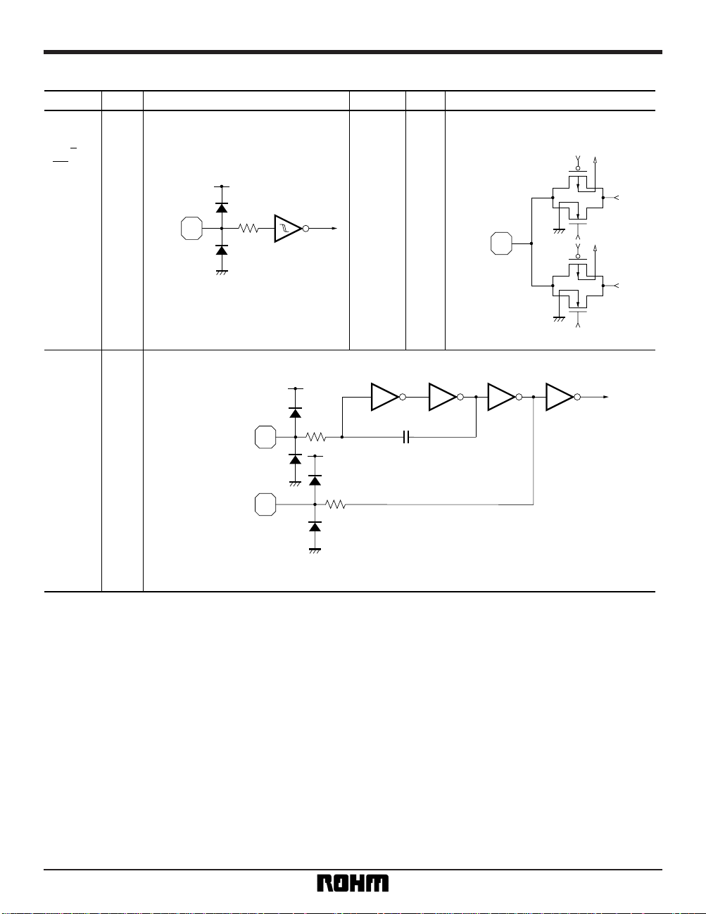
Input / output circuits
Pin name I / O Equivalent circuit Pin name
COM1
~
COM4
GND
V
DD
IN
I / O Equivalent circuit
OSC1
OSC2
SD
SCK
C / D
CS
I
O
I SEG1
~
SEG18
O
GND
V
DD
OSC1
OSC2
VLCD
OUT
GND
VLCD
Page 6
6
Standard ICs BU9729K
•
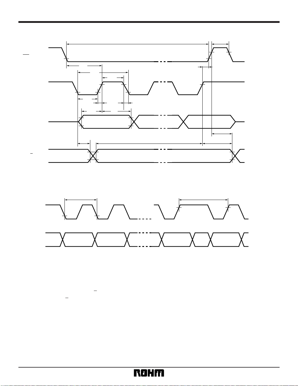
Timing charts
C / D
CS
SCK
t
WL2 tWH2
SD
SCK
D
7
SD
tH2
D6
D0
D7
tSU2
tWH1
tWL1
tSCH
tCYC
tSU3 tH3
tCCH
tSU1 tH1
tTLH1 tTHL
tCYC
tWA / T
Fig. 2 Interface timing
Fig. 3 Command cycle
•
Data format
Serial data is transmitted using four-line clock synchronous transmission. Serial data with a length of eight bits is
input synchronized to SCK. If C / D is HIGH at the rise of the 8 × nth clock of SCK, the serial data is recognized as a
command, and if C / D is LOW, the serial data is recognized as display data.
Serial data is input sequentially, starting from the MSB.
Page 7
7
Standard ICs BU9729K
•
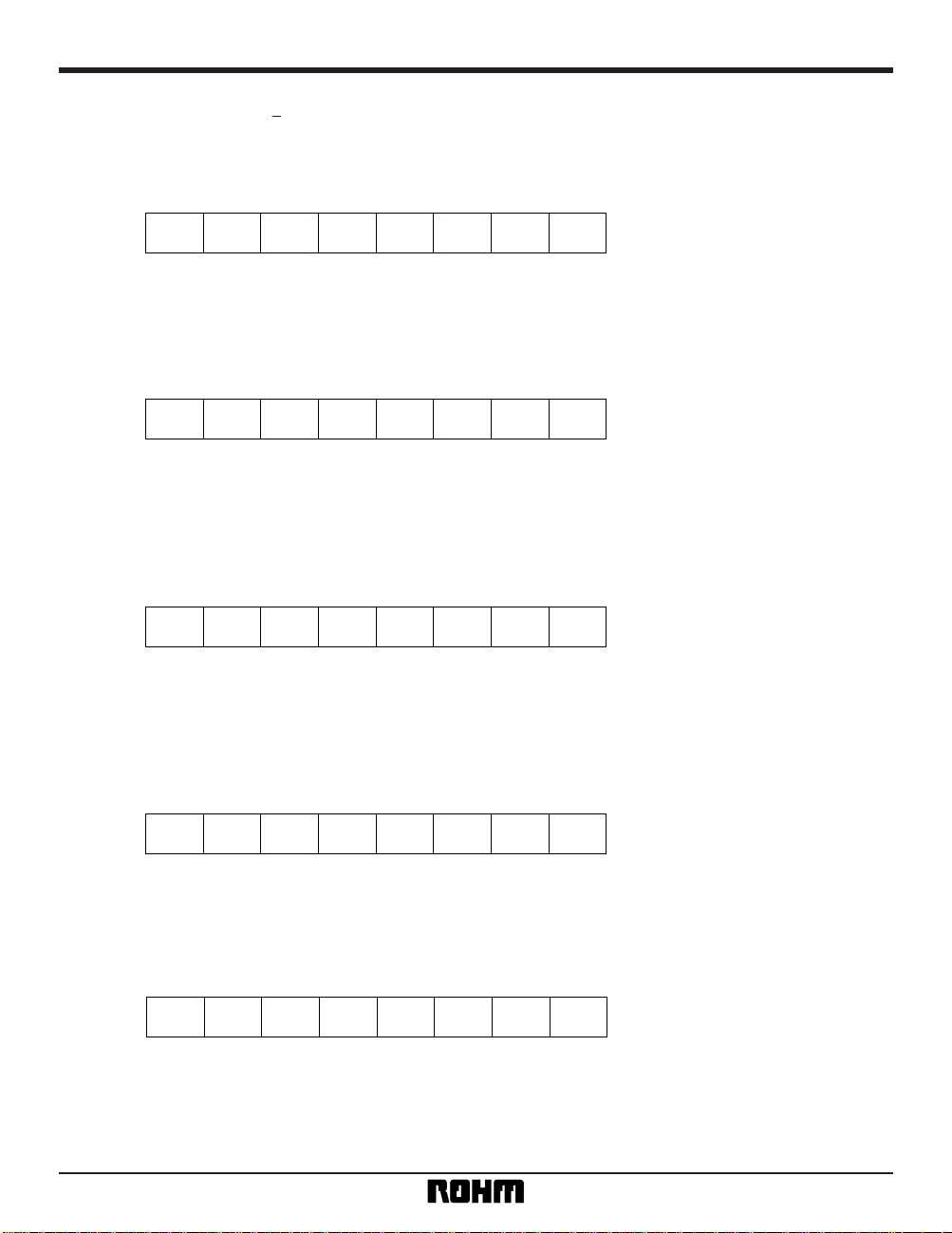
Detailed explanation of commands
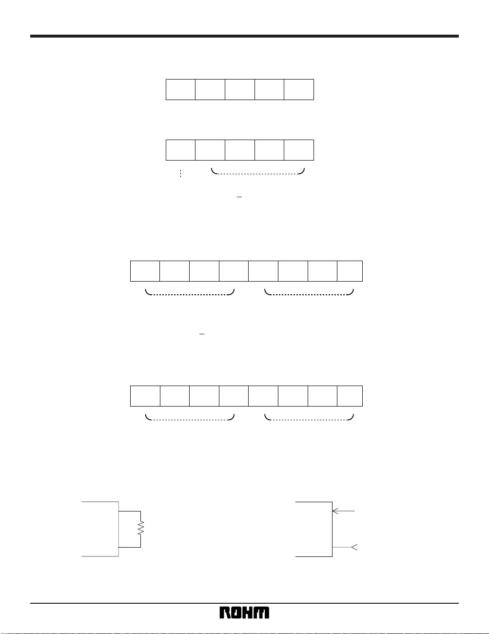
The following commands (C / D is HIGH at the 8 × nth clock of SCK) are available for the BU9729K.
(1) Address Set
0 00AAAAA
LSBMSB
Address data displayed in binary format as AAAAA is set for the address counter.
The address is incremented by two each time input of the display data (8 bits of data) is completed.
(2) Display On
0 01
LSB
∗
: Don't Care
MSB
∗∗∗∗∗
All displays light, regardless of the contents of the display data RAM (DDRAM). At this point, the contents of the
DDRAM do not change.
(3) Display Off
0 10
LSB
∗
: Don't Care
MSB
∗∗∗∗∗
All displays go out, regardless of the contents of the DDRAM.
At this point, the contents of the DDRAM do not change.
(4) Display Start
0 11
LSB
∗
: Don't Care
MSB
∗
∗∗∗∗
The display begins, in accordance with the contents of the DDRAM.
(5) Display Data RAM (DDRAM) Write
1 00 DDDD
LSB
∗
: Don't Care
MSB
∗
The binary 4-bit data DDDD is written to the DDRAM.
The address is that specified by the Address Set command. After this command is executed, the address is automatically incremented by + 1.
Page 8
8
Standard ICs BU9729K
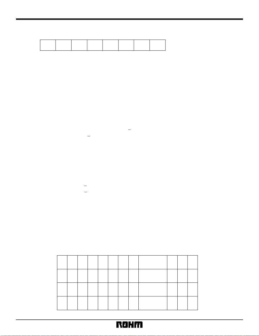
(6) Reset
1 10
∗
LSB
∗
: Don't Care
MSB
∗∗∗∗
This command should be executed after the power supply has been turned on and before any other command is
executed. This command causes the BU9729K to initialize the following:
Display Off
Address Counter Reset
•
Description of functions
(1) Register
The BU9729K has an 8-bit command / data register. Serial data is read in 8-clock units of SCK.
If the data read into the register is displayed data (C / D is LOW at the eighth clock of SCK), it is written to the
DDRAM. If it is command data (C / D is HIGH at the eighth clock of SCK), it is output to the command decoder to
control the BU9729K.
(2) Address counter
The address counter indicates DDRAM addresses. When the Address Set command is written to a command or data
register, the address data is sent automatically to the address counter.
After data has been written to the DDRAM, the address counter increments automatically by either + 1 or + 2. The
amount by which the counter increments is determined automatically, based on the following status.
DDRAM 8-bit writing (C / D is LOW at the eighth clock of SCK) → + 2
DDRAM 4-bit writing (C / D is HIGH at the eighth clock of SCK) → + 1
When the address counter has counted to the address 11H, it becomes 00H the next time it is incremented.
(3) Display data RAM (DDRAM)
The display data RAM (DDRAM) is used to store display data. It has a capacity of 18 addresses × 4 bits.
The relationship between the DDRAM and the display position is shown below.
DD RAM address
00
11100F01 02 03 04 05 06 07 ·········
1
2
3
0
COM2
COM3
COM4
COM1
Page 9
9
Standard ICs BU9729K
DDRAM addresses set for the address counter are in hexadecimal format, and are displayed as shown below.
AC4 AC3 AC2 AC1 AC0
LSBMSB
(Example) When the DDRAM address is "11" (display position: SEG18)
1
1
0001
LSBMSB
1
Display data input to the command / data register (C / D = LOW) is divided into the first four bits and the last four
bits, with the specified DDRAM address being written to the first four, and the specified address + 1 being written to
the last four. The four bits of display data are written sequentially to the bits of the DDRAM, starting from the MSB on
both sides.
Specified address
(bit3 bit0)
Specified address + 1
(bit3 bit0)
D7 D6 D5 D4 D3 D2 D1 D0
LSBMSB
When a DDRAM Write command is input (C / D = HIGH), the four bits of display data in the DDRAM Write command
are written to the specified DDRAM address. The four bits are written sequentially, starting from the MSB, to the bits
of the DDRAM, starting with the MSB of the DDRAM.
DDRAM Write command Display data
(bit3 bit0)
1 00
∗
D3 D2 D1 D0
LSBMSB
(4) Timing generator
Connecting Rf between OSC1 and OSC2 causes oscillation of the internal oscillator circuit and generates a display
timing signal. Operation can also be initiated by inputting an external clock.
OSC1
OSC2
Rf
(Rf can be used
to change the
oscillation
frequency.)
Fig. 4 Rf oscillator circuit
OSC1
OSC2
EXIT CLOCK INPUT
Fig. 5 External clock input
OPEN
Page 10
10
Standard ICs BU9729K
(5) LCD driver power supply
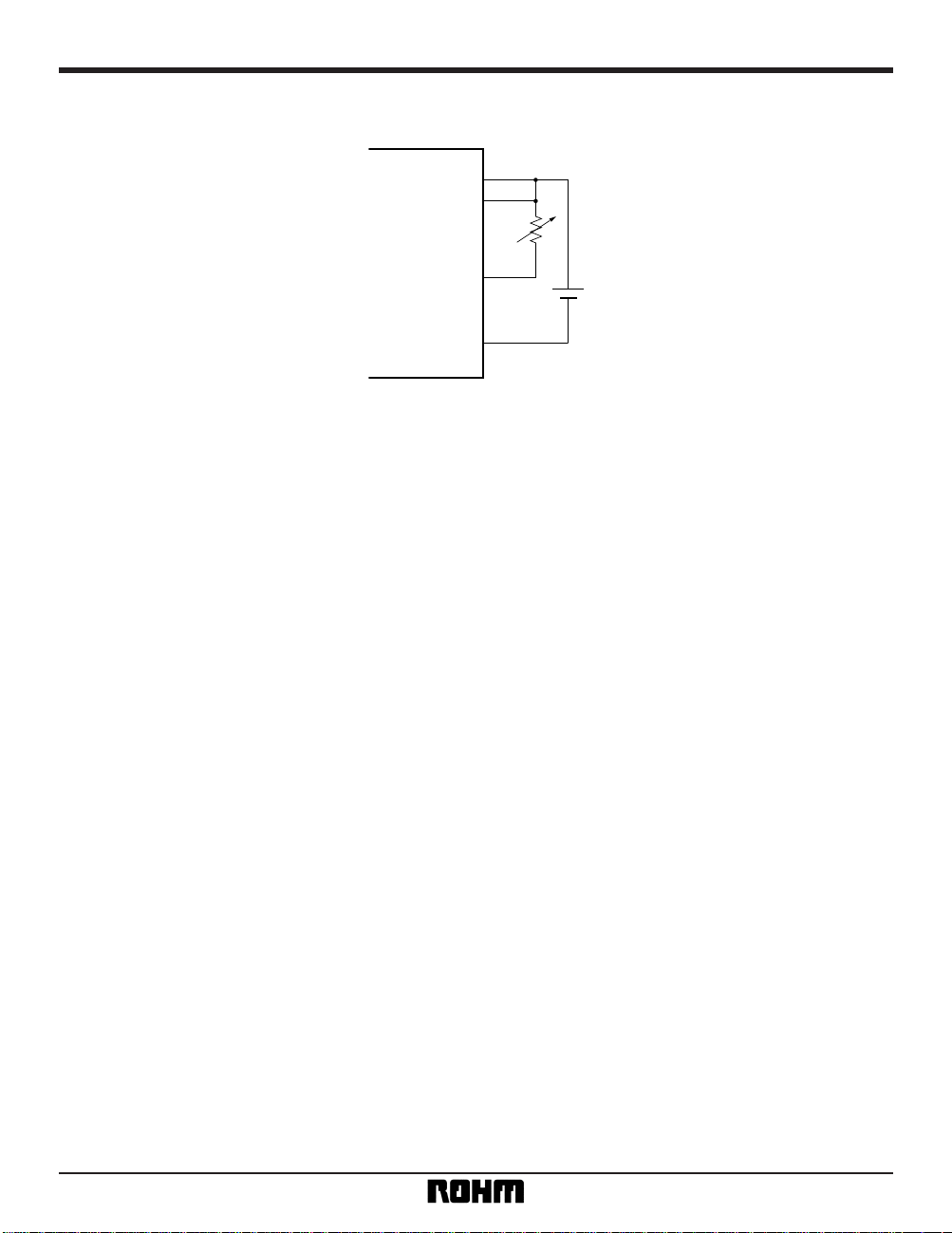
The LCD driver power supply is generated by the BU9729K. V
1 = 2 · VC / 3, V2 = VC / 3 is generated internally.
VDD
VLCD
VC
VSS
Fig. 6 Example of power supply connection
(6) LCD drive circuit
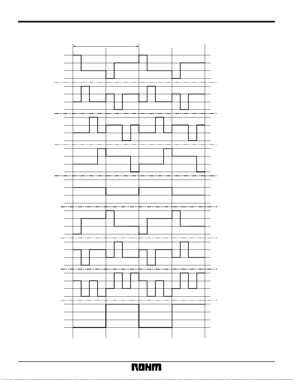
The LCD drive circuit is configured of 4 common drivers and 18 segment drivers. When oscillation begins, any effective common output automatically outputs a selective waveform, while the others output non-selective waveforms.
Segment output automatically outputs drive waveforms, based on the display data and common counter. The common and segment output waveforms are shown in the following examples.
Page 11
11
Standard ICs BU9729K
•
LCD drive waveforms
COM1
V
C
V1
V2
VSS
Frame interval
COM2
V
C
V1
V2
VSS
COM3
V
C
V1
V2
VSS
COM4
V
C
V1
V2
VSS
VC
V1
V2
VSS
VC
V1
V2
VSS
SEG1
SEG18
~
VC
V1
V2
VSS
VC
V1
V2
VSS
VC
V1
V2
VSS
COM1 COM2 COM3 COM4
0 0 0 0
(No SEGn corresponding
from COM1 to COM4 are
displayed.)
1 0 0 0
(Only SEGn corresponding
to COM1 are displayed.)
0 1 0 0
(Only SEGn corresponding
to COM2 are displayed.)
0 1 0 1
(Only SEGn corresponding
to COM2 and COM4 are
displayed.)
1 1 1 1
(All SEGn corresponding
from COM1 to COM4 are
displayed.)
Fig. 7
Page 12
12
Standard ICs BU9729K
•
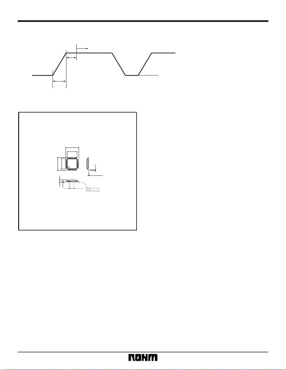
External dimensions (Units: mm)
QFP32
0.15
0.4
±
0.1
24
17
16
9
8
1
25
32
7.0
±
0.2
9.0
± 0.3
7.0
±
0.2
9.0
± 0.3
0.4
0.05
1.45
±
0.1
0.15
± 0.1
0.8
0 < tON < 10ms
V
DD ⭌ 2.5V
V
DD < 0.3V
t
WAIT < 1ms
Instruction receipt possible
V
DD has to satisfy the following conditions.
 Loading...