

Page 1
1
Standard ICs
Picture cell driver for STN (LCD driver)
for low voltage power supplies
BU9718KV
The BU9718KV is a driver IC designed for the character-type STN liquid crystal panels which are ideal for applications such as portable devices. The number of display segments includes 32 output segments and 3 common outputs, enabling drive of up to 96 segments. A compact 48-pin QFP package with a pitch of 0.5 mm is used, enabling
compact size for the set as a whole.
•
Features
1) Operates on 3V power supply.
2) Low current dissipation. (0.1µA in low power mode
(actual value))
3) Compact package. (molded section is 7.0 mm
ⵧ
)
4) Up to 32 segment output pins and 3 common output
pins are provided, enabling a total display of up to
96 segments.
5) 1 / 3 duty display.
6) Either 1 / 2 or 1 / 3 bias can be selected for power supplyfor LCD display.
•
Applications
Portable terminals (POS, ECR, PDA, and others),
movie projectors, cameras, telephones (cordless hand-
held telephone units), and others Low-voltage power
supply sets
•
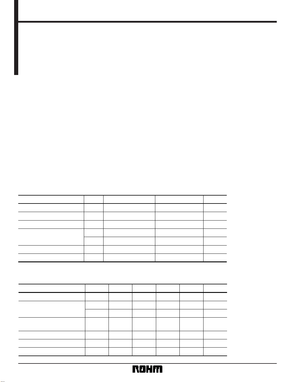
Absolute maximum ratings (Ta = 25°C, VSS = 0V)
Parameter
Power supply voltage
∗
1
Input voltage
∗
1
Output voltage
∗
1
Output current
V
DD
VIN
VOUT
ISO
– 0.3 ~ + 7.0
– 0.3 ~ V
DD + 0.3
– 0.3 ~ V
DD + 0.3
300
V
Symbol
V
DD
OSC, CS, CK, DI, RES
OSC
S
1 ~ S32
Pin Limits Unit
V
V
µA
ICO 3COM1 ~ COM3 mA
Power dissipation Pd 400
∗
2
—mW
Storage temperature Tstg – 55 ~ + 125— °C
∗
1 Max. voltage that can be applied with a VSS pin
∗
2 Reduced by 4.0mW for each increase in Ta 1°C over 25°C.
•
Recommended operating conditions (Ta = 25°C, VSS = 0V)
Parameter
Power supply voltage
∗
VDD V
Symbol
VDD
Pin
2.7
Min.
—
Typ.
3.5
Input voltage
∗
Oscillation freq., with
external input
V
DD1 VVDD1 0 2 / 3 VDD VDD
VDD2 VVDD2 0 1 / 3 VDD VDD
fOSC kHzOSC — 38 100
External resistance R kΩOSC — 47 —
External capacitance C pFOSC — 1000 —
Operating temperature Topr °C— – 40 — 85
Max. Unit
∗
Indicates the max. voltage that can be applied with a VSS pin.
Page 2
2
Standard ICs BU9718KV
•
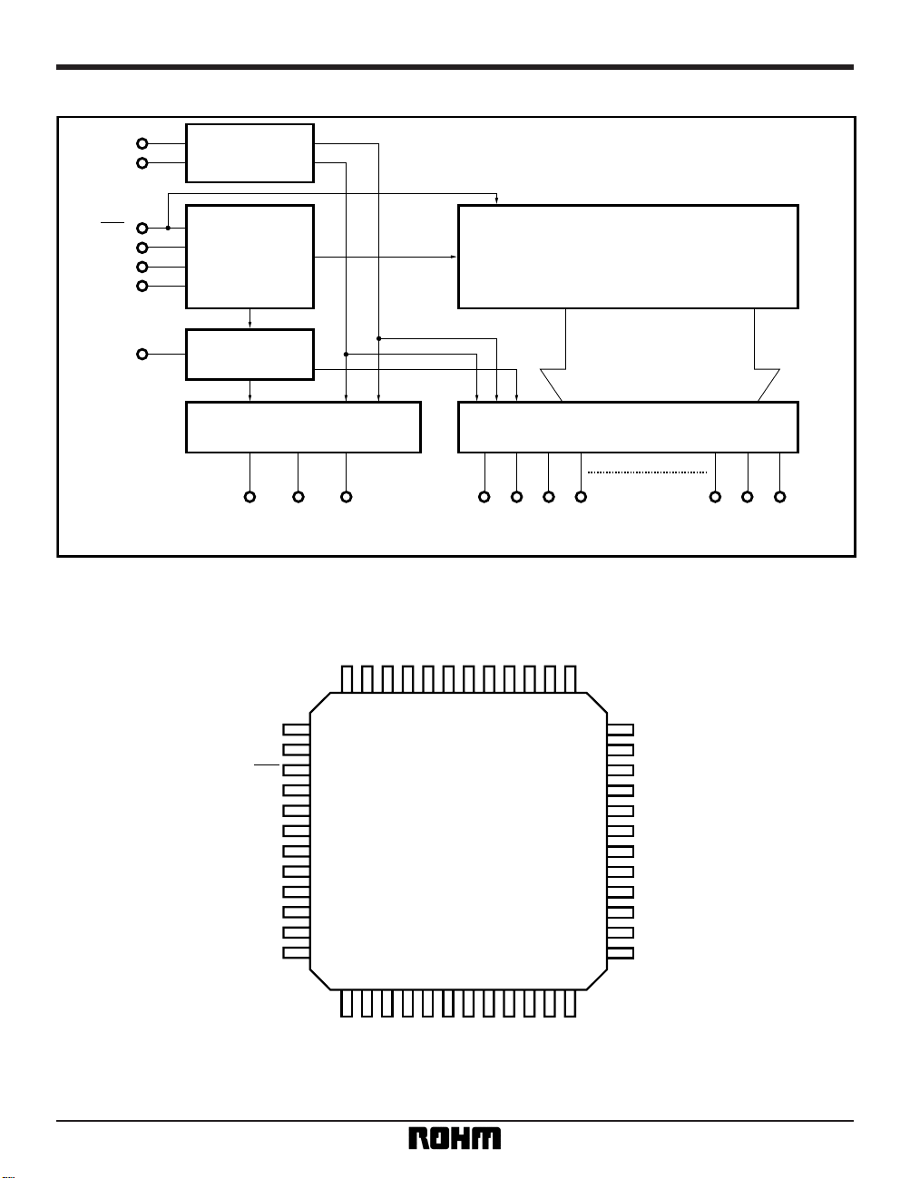
Block diagram
Segment Driver
Data Latch
CTRL Logic
OSC
Common Driver
V
DD1
VDD2
RES
DI
CS
CK
OSC
COM1
COM2
COM3
S1
S2
S3
S4
S30
S31
S32
LCD Power
•
Pin assignments
VQFP48
36 25
121
37
48
24
13
COM1
S32
S31
S30
S29
S28
S27
S26
S25
S24
S23
N.C.
S
1
S2
S3
S4
S5
S6S7S8
S9
S10
S11
N.C.
COM2
COM3
RES
V
DD
VDD1
VDD2
VSS
OSC
CS
CK
DI
N.C.
N.C.
S
22
S21
S20
S19
S18
S17
S16
S15
S14
S13
S12
Page 3
3
Standard ICs BU9718KV
•
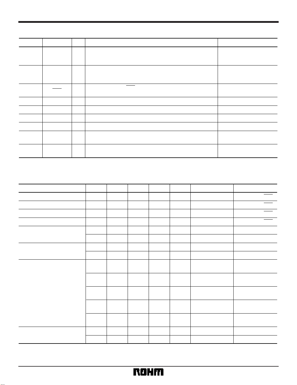
Pin descriptions
Pin No.
1—11
13—23
26—35
Pin name
S
23—S32
S12—S22
S1—S11
Segment data output pin; outputs LCD drive voltage that
matches COM
1 - COM3 compatible data
I / O
O
Function Processing when not in use
44 OSC — Oscillation pin (for common, segment alternation waves) VSS
45 CS I Chip segment input; when CS = H, data can be transferred VSS
46 CK I Synchronous clock input for serial data transfer VSS
47 DI I Serial data input VSS
OPEN
36
37
38 COM
3
COM2
COM1
Common drive output; frame freq. fC = (fOSC / 384) HzO
V
SS
39
I
VDD
RES
Reset input; when RES = L, resets internal data
(include. control data)
41
—
OPEN
V
DD1
Internal standard voltage for liquid-crystal drive; when using
1 / 2 bias mode, connects to V
DD2
42
—
OPEN
V
DD2
Internal standard voltage for liquid-crystal drive; when using
1 / 2 bias mode, connects to V
DD1
•
Electrical characteristics (unless otherwise noted, Ta = 25°C, VDD = 2.7V to 3.5V, VSS = 0V)
Parameter Symbol Min. Typ. Max. Unit Conditions Pin
Input high level voltage VIH 0.8 VDD —VDD V — CS, CK, DI, RES
CS, CK, DI, RES
CS, CK, DI, RES
CS, CK, DI, RES
Input low level voltage VIL 0 — 0.2 VDD V—
Input high level current IIH 0 — 6.0 µAVI = VDD
Input low level current IIL 0 — 6.0 µAVI = VSS
Output high level voltage
V
SOH —VDD – 1.0 — V IO = – 20µAS1 ~ S32
VCOH —VDD – 1.0 — V IO = – 100µA COM1 ~ COM3
Output low level voltage
Output medium level voltage
V
SOL — 1.0 — V IO = 20µAS1 ~ S32
VCOL — 1.0 — V IO = 100µA COM1 ~ COM3
Power supply current
I
Q — 0.1 30 µA Low-power mode —
IDD — 100 300 µAfOSC = 38kHz —
V
CM1 —
1 / 2 V
DD
± 1.0
— V 1 / 2bias COM
1 ~ COM3
VSM1 —
2 / 3 V
DD
± 1.0
— V 1 / 3bias S
1 ~ S32
VCM2 —
2 / 3 V
DD
± 1.0
— V 1 / 3bias COM
1 ~ COM3
VSM2 —
1 / 3 V
DD
± 1.0
— V 1 / 3bias S
1 ~ S32
VCM3 —
1 / 3 V
DD
± 1.0
— V 1 / 3bias COM
1 ~ COM3
Page 4

4
Standard ICs BU9718KV
•
AC characteristics (unless otherwise noted, Ta = 25°C, VDD = 2.7V to 3.5V, VSS = 0V)
Parameter Symbol Min. Typ. Max. Unit Conditions Pin
Guaranteed oscillation range
Operating frequency
Data set-up time
Data hold time
CS set-up time
CS hold time
CK "H" level pulse width
CK "L" level pulse width
Rise time
Fall time
f
OSC 10 38 80 kHz C = 1000pF R = 47kΩ
External input
OSC
fOSC — — 100 kHz OSC
tDS 200 — — ns CK, DI
tDH 200 — — ns CK, DI
tCS 200 — — ns CS, CK
tCH 200 — — ns CS, CK
tCKH 200 — — ns CK
tCKL 200 — — ns CK
tr — — 100 ns CS, CK, DI
tf — —
—
—
—
—
—
—
—
—100 ns CS, CK, DI
AC timing waveform
(1) When CK is stopped at “L”
(2) When CK is stopped at “H”
0.8VDD
0.8VDD
CS
CK
DI
0.8V
DD
0.8VDD
0.2VDD
0.5VDD 0.5VDD
0.2VDD
tCS
tDS tDH tr tf
t
CKH tCKL tCH
CS
CK
DI
0.2V
DD
0.8VDD
0.2VDD
0.5VDD 0.5VDD
0.2VDD
tCS
tDS tDH tr tf
t
CKH tCKL tCH
Fig.1
Fig.2
Page 5

5
Standard ICs BU9718KV
Timing charts
(1) When CK is stopped at “L”
CS
CK
DI
D1 D2
Display data Control code
D3
D95 0 0 0 0 0 BM LC OE
Fig.3
When CS is HIGH, data can be transferred. Data is sent to the shift register at the rising edge of CK. After all of the
DI data has been transferred, CS should be set to LOW. The voltage corresponding to the display data transferred at
the falling edge of CS is output.
(2) When CK is stopped at “H”
CS
CK
DI
D1 D2
Display data Control code
D3
D96 0 0 0 0 0 BM LC OE
Fig.4
Control code table
Output enable control
Normal operation
No display; all display data = 0 (internal oscillation circuit is operating)
OE
0
1
Low-power mode control
Normal operation
Low-power mode = internal oscillation circuit has stopped; segment and common output = 0
LC
0
1
Bias mode control
1 / 3 bias
1 / 2 bias
BM
0
1
Page 6

6
Standard ICs BU9718KV
Correspondence between display data input and segments
S1 D1
D2
D3
S2
D4
D5
D6
S3
D7 D8
D9
S4
D10
D11
D12
S5
D13
D14
D15
S6
D16 D17
D18
S7 D19
D20 D21
S8 D22
D23
D24
S9
D25
D26
D27
S10
D28
D29
D30
S11
D31
D32
D33
S12
D34
D35
D36
S13
D37
D38
D39
S14
D40
D41 D42
S15
D43
D44
D45
S16
D46
D47 D48
Segment COM3 COM2 COM1 Segment COM3 COM2 COM1
S17 D49 D50 D51
S18 D52 D53 D54
S19 D55 D56 D57
S20 D58 D59 D60
S21 D61 D62 D63
S22 D64 D65 D66
S23 D67 D68 D69
S24 D70 D71 D72
S25 D73 D74 D75
S26 D76 D77 D78
S27 D79 D80 D81
S28 D82 D83 D84
S29 D85 D86 D87
S30 D88 D89 D90
S31 D91 D92 D93
S32 D94 D95 D96
Page 7

7
Standard ICs BU9718KV
•
Output waveforms
VDD
fO = fOSC / 384 fO = fOSC / 384
V
DD1, VDD2
VSS
VDD
VDD1
VDD2
VSS
VDD
VDD1
VDD2
VSS
VDD
VDD1
VDD2
VSS
VDD
VDD1
VDD2
VSS
VDD
VDD1
VDD2
VSS
VDD
VDD1
VDD2
VSS
VDD
VDD1
VDD2
VSS
VDD
VDD1
VDD2
VSS
VDD
VDD1
VDD2
VSS
VDD
VDD1
VDD2
VSS
VDD
VDD1
VDD2
VSS
VDD
VDD1, VDD2
VSS
VDD
VDD1, VDD2
VSS
VDD
VDD1, VDD2
VSS
VDD
VDD1, VDD2
VSS
VDD
VDD1, VDD2
VSS
VDD
VDD1, VDD2
VSS
VDD
VDD1, VDD2
VSS
VDD
VDD1, VDD2
VSS
VDD
VDD1, VDD2
VSS
VDD
VDD1, VDD2
VSS
1 / 2 bias 1 / 3 duty waveform 1 / 3 bias 1 / 3 duty waveform
COM
1
COM2
COM3
LCD driver output, when all LCD segments for
COM
1, 2 and 3 are out
LCD driver output, when all the LCD segments
for COM
1, 2 and 3 are lit up
LCD driver output, when the LCD segments for
COM
1 and 2 are lit up
LCD driver output, when the LCD segments for
COM
1 and 3 are lit up
LCD driver output, when the LCD segments for
COM
2 and 3 are lit up
LCD driver output, when only the LCD segment
for COM
1 is lit up
LCD driver output, when only the LCD segment
for COM
2 is lit up
LCD driver output, when only the LCD segment for
COM
3 is lit up
Fig.5 Fig.6
Page 8

8
Standard ICs BU9718KV
•
Application example 1
COM1VDDVDD
VDD1
VDD2
VSS
RES
BU9718KV
1 / 2 bias mode
1 / 3 bias mode
96
Segment
LCD
Controller
C ⭌ 0.047µF
CS
CK
DI
OSC
47kΩ
GND
1000pF
COM
2
COM3
S1
S2
S3
S4
S6
S5
S32
VDD
BU9718KV
96
Segment
LCD
Controller
C ⭌ 0.047µF
47kΩ
GND
1000pF
COM1VDD
VDD1
VDD2
VSS
RES
CS
CK
DI
OSC
COM
2
COM3
S1
S2
S3
S4
S6
S5
S32
Fig.7
Fig.8
Page 9

9
Standard ICs BU9718KV
•
Application example 2
VDD
∗
1)
∗
2)
V
DD
R
R
R
R
R
BU9718KV
1 / 2 bias mode
1 / 3 bias mode
96
Segment
LCD
Controller
C ⭌ 0.047µF
47kΩ
GND
1000pF
BU9718KV
96
Segment
LCD
Controller
C ⭌ 0.047µF
47kΩ
GND
1000pF
COM1VDD
VDD1
VDD2
VSS
RES
CS
CK
DI
OSC
COM
2
COM3
S1
S2
S3
S4
S6
S5
S32
COM1VDD
VDD1
VDD2
VSS
RES
CS
CK
DI
OSC
COM
2
COM3
S1
S2
S3
S4
S6
S5
S32
Fig.9
Fig.10
Note: The resistance values and capacitance for ∗1 and ∗2 should be set to match the LCD panel, and should be checked using test operation.
Page 10

10
Standard ICs BU9718KV
•
External dimensions (Units: mm)
0.5
0.125 ± 0.1
0.10
0.2
±
0.1
9.0 ± 0.3
7.0
±
0.2
9.0 ± 0.3
7.0
±
0.2
48
37
1
12
13
24
2536
0.5
1.425
±
0.1
0.10
VQFP48
Make sure of the following when resetting when the power is on.
• When using the external reset terminal, make RST = “L” at 1 ms or more with V
DD at 2.7V or more.
• When not using the external reset terminal,V
DD has to satisfy the following conditions.
0 < tON < 10ms
V
DD ⭌ 2.7V
V
DD < 0.3V
t
WAIT ⭌ 1ms
Instruction receipt possible
 Loading...