

BD243B/BD243C
BD244B/BD244C
COMPLEMENTARY SILICON POWER TRANSISTORS
■ STMicroelectronicsPREFERRED
SALESTYPES
DESCRIPTION
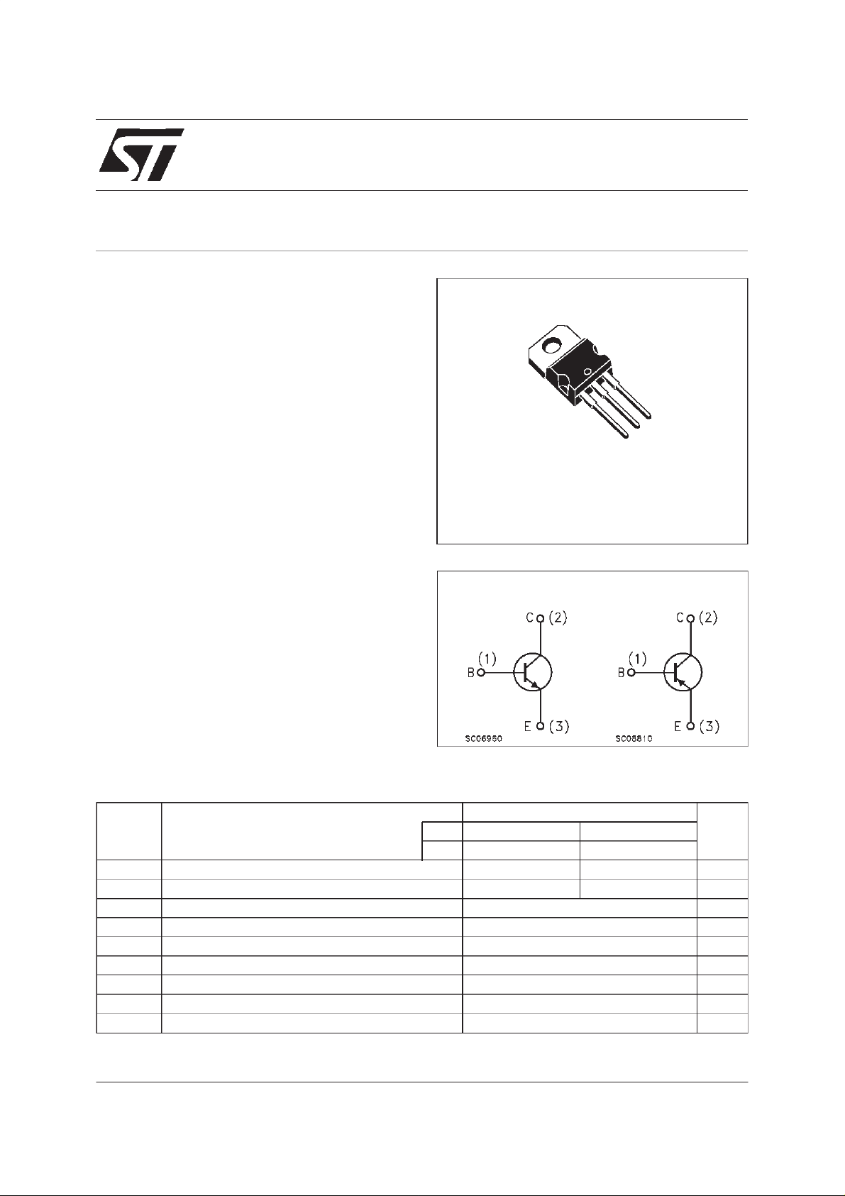
The BD243B and BD243C are silicon
Epitaxial-BaseNPN transistors mounted in Jedec
TO-220plastic package.
They are inteded for use in medium power linear
and switching applications.
The complementaryPNP types are BD244B and
BD244C respectively.
TO-220
3
2
1
INTERNAL SCHEMATIC DIAGRAM
ABSOLUTE MAXIMUM RATINGS
Symbol Parameter Value Unit
NPN BD243 B BD243 C
PNP BD244 B BD244 C
V
V
V
I
P
T
For PNP types voltage and current values are negative.
Collector-Base Voltage (IE=0) 80 100 V
CBO
Collector-Emitter Voltage (IB=0) 80 100 V
CEO
Emitter-Base Voltage (IC=0) 5 V
EBO
Collector Current 6 A
I
C
Collector Peak Current 10 A
CM
Base Current 2 A
I
B
Tot al Dissipation at Tc≤ 25oC
tot
Sto rage T em pe rature -65 to 150
stg
Max. Oper at in g Junctio n T emper at u re 150
T
j
65 W
o
C
o
C
September 1999
1/4
BD243B / BD243C / BD244B/ BD244C
THERMAL DATA
R
thj-case
R
thj-amb
Ther mal Resist ance Junctio n-c a s e Ma x
Ther mal Resist ance Junctio n-ambient Max
1.92
62.5
o
C/W
o
C/W
ELECTRICAL CHARACTERISTICS (T
=25oC unlessotherwise specified)
case
Symbol Parameter Test Condition s Min. Typ. M ax. Unit
I
CES
I
CEO
I
EBO
V
CEO(sus)
V
CE(sat)
Collec t or Cut -off
Current (V
BE
=0)
Collec t or Cut -off
Current (I
B
=0)
Emitt er Cut-of f Current
(I
=0)
C
∗ Co llec t or -Emit t er
Sust aining Voltage
=0)
(I
B
∗ Collec t or -Emit t er
V
=ratedV
CE
V
=60V 0.7 mA
CE
=5V 1 mA
V
EB
I
=30mA
C
for BD243B/ B D244B
for BD243C/ B D244C
CEO
80
100
0.4 mA
IC=6A IB=1A 1.5 V
Saturation Voltage
∗ Base-Emi tter Voltage IC=6A VCE=4V 2 V
V
BE
h
∗ DC Current Ga in IC=0.3A VCE=4V
FE
h
Small Signa l Cu rr en t
fe
Gain
∗
Pulsed: Pulse duration= 300µs, duty cycle ≤ 2%
For PNPtypes voltage and current values are negative.
=3A VCE=4V
I
C
IC=0.5A VCE=10V f=1MHz
=0.5A VCE=10V f=1KHz320
I
C
30
15
V
V
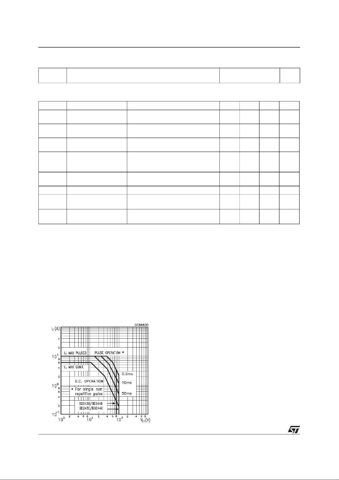
Safe Operating Area
2/4

BD243B/ BD243C/ BD244B / BD244C
TO-220 MECHANICAL DATA
DIM.
MIN. TYP. MAX. MIN. TYP. MAX.
A 4.40 4.60 0.173 0.181
C 1.23 1.32 0.048 0.051
D 2.40 2.72 0.094 0.107
D1 1.27 0.050
E 0.49 0.70 0.019 0.027
F 0.61 0.88 0.024 0.034
F1 1.14 1.70 0.044 0.067
F2 1.14 1.70 0.044 0.067
G 4.95 5.15 0.194 0.203
G1 2.4 2.7 0.094 0.106
H2 10.0 10.40 0.393 0.409
L2 16.4 0.645
L4 13.0 14.0 0.511 0.551
L5 2.65 2.95 0.104 0.116
L6 15.25 15.75 0.600 0.620
L7 6.2 6.6 0.244 0.260
L9 3.5 3.93 0.137 0.154
DIA. 3.75 3.85 0.147 0.151
mm inch
P011C
3/4

BD243B / BD243C / BD244B/ BD244C
Information furnished isbelieved to beaccurate and reliable. However, STMicroelectronics assumes noresponsibility for the consequences
of use of such information nor for any infringement of patents or other rights of third parties which may result from its use. No license is
granted by implication orotherwise underany patent or patentrights of STMicroelectronics. Specification mentioned inthis publication are
subject tochange without notice.This publication supersedes andreplaces allinformation previously supplied. STMicroelectronics products
are not authorized for use as critical components in life support devices or systems without express written approval of STMicroelectronics.
The ST logo is a trademark of STMicroelectronics
1999 STMicroelectronics – Printedin Italy– AllRights Reserved
STMicroelectronicsGROUP OF COMPANIES
Australia - Brazil -China - Finland - France - Germany- HongKong - India- Italy- Japan -Malaysia - Malta - Morocco -
Singapore- Spain - Sweden - Switzerland -United Kingdom -U.S.A.
http://www.st.com
.
4/4
 Loading...