

BAS70J / BAS70W
BAS70-04W /BAS70-05W / BAS70-06W
SMALL SIGNAL SCHOTTKY DIODE
FEATURES AND BENEFITS
n VERY SMALL CONDUCTIONLOSSES
n NEGLIGIBLE SWITCHING LOSSES
n LOW FORWARD VOLTAGE DROP
n SURFACE MOUNT DEVICE
DESCRIPTION
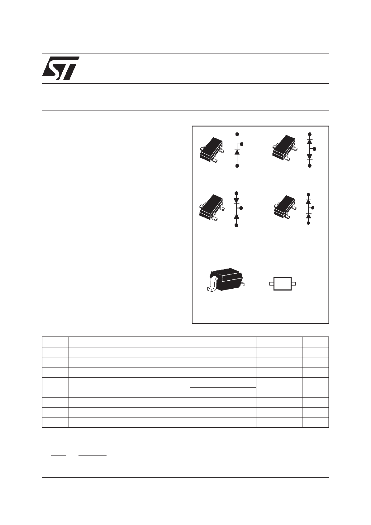
Schottky barrier diodes encapsulated either in
SOT-323 orSOD-323 small SMD packages.
Single and double diodes with different pining are
available.
K
A
BAS70W
K
A1
BAS70-05W
NC
A2
NC
K
A
A2
K
A1
SOT-323
A
K1
BAS70-06W
A2
K1
A1
BAS70-04W
K2
K2
K2
A
K1
K2
A2
K1
A1
76
A
K
BAS70J
SOD-323
ABSOLUTE RATINGS (limiting values)
Symbol Parameter Value Unit
V
I
RRM
FSM
P
T
Repetitive peakreverse voltage 70 V
I
Continuous forward current 70 mA
F
Surge non repetitive forward current tp = 10 ms 1 A
Power dissipation (note 1)
tot
Tamb = 25°C
Maximum storage temperature range - 65 to +150 °C
stg
SOD-323 230 mW
SOT-323
Tj Maximum operating junction temperature * 150 °C
T
Note 1: for doublediodes, Ptot is the total dissipation of both diodes.
dPtot
*:
Maximum temperature for soldering during 10s 260 °C
L
<
dTj Rth j a
thermal runaway condition for a diode on its own heatsink
−1()
May 2000 - Ed: 4B
1/5
BAS70J / BAS70W / BAS70-04W / BAS70-05W / BAS70-06W
THERMAL RESISTANCE
Symbol Parameters Value Unit
R
th (j-a)
Junction to ambient (*) SOD-323 550 °C/W
SOT-323 °C/W
(*) Mounted on epoxy board, with recommended pad layout.
STATIC ELECTRICAL CHARACTERISTICS (per diode)
Symbol Test Conditions Min. Typ. Max. Unit
V
BR
V
F
IR** Tj = 25°CV
Pulse test: * tp = 380µs, δ <2%
Tj = 25°CI
*Tj=25°CI
** tp = 5 ms, δ <2%
=10µA70V
R
= 1mA 410 mV
F
= 50V 100 nA
R
DYNAMIC CHARACTERISTICS
Symbol Test Conditions Min. Typ. Max. Unit
CTj=25°CV
=0V
R
2pF
F = 1MHz
τ*Tj=25°CI
Krakauer Method
* Effective carrier lifetime.
= 5mA
F
100 ps
2/5
BAS70J / BAS70W / BAS70-04W /BAS70-05W / BAS70-06W
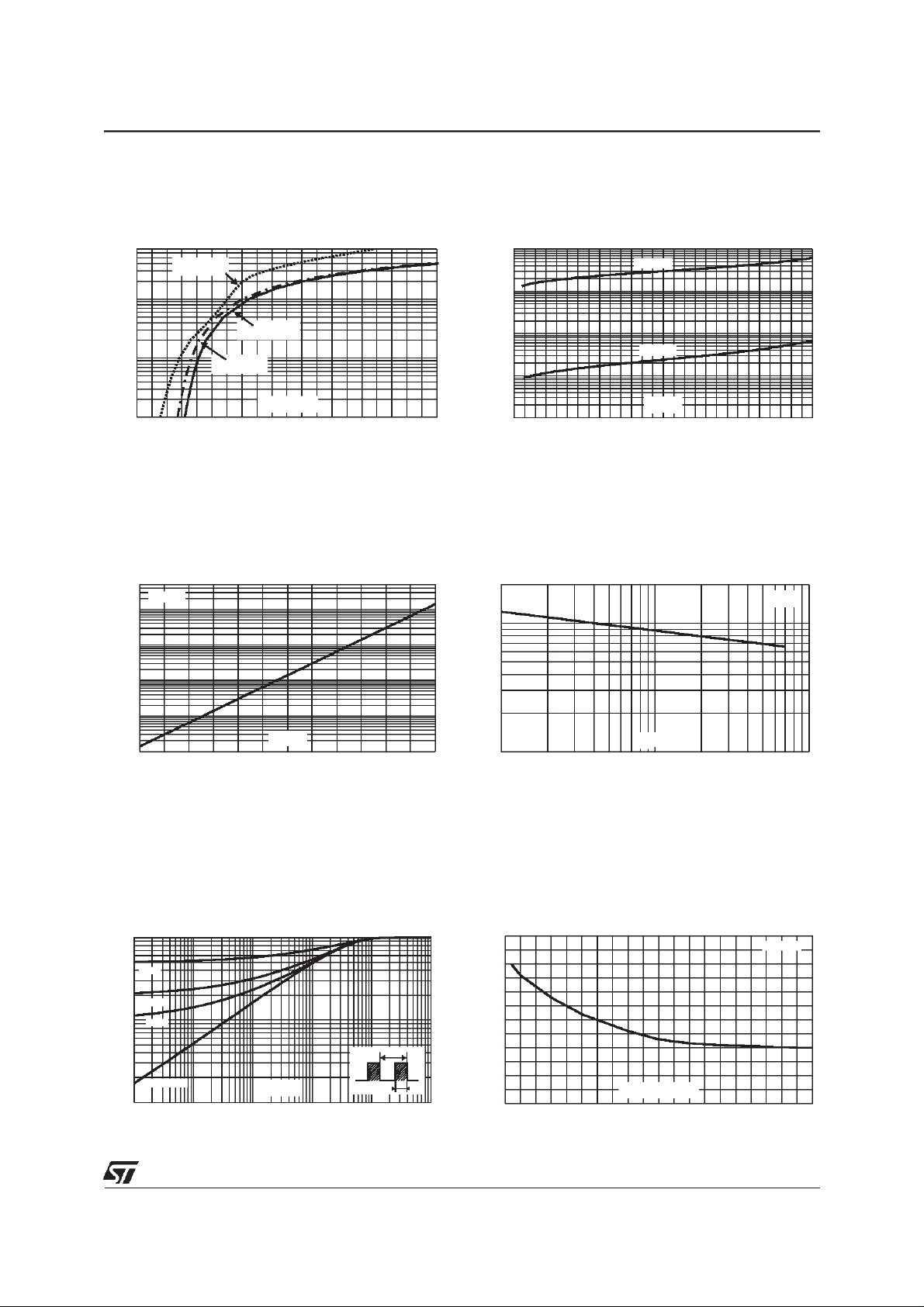
Fig. 1: Forward voltage drop versus forward
current.
IFM(A)
7E-2
Tj=100°C
Typicalvalues
1E-2
Tj=25°C
Maximum values
1E-3
Tj=25°C
Typicalvalues
VFM(V)
1E-4
0.0 0.2 0.4 0.6 0.8 1.0 1.2 1.4 1.6 1.8 2.0
Fig. 3: Reverse leakage current versus junction
temperature (typicalvalues).
IR(µA)
5E+2
1E+2
1E+1
VR=70V
Fig. 2: Reverse leakage current versus reverse
voltage applied (typical values).
IR(µA)
1E+1
Tj=100°C
1E+0
1E-1
Tj=25°C
1E-2
VR(V)
1E-3
0 5 10 15 20 25 30 35 40 45 50 55 60 65 70
Fig. 4: Junction capacitance versus reverse
voltage applied (typical values).
C(pF)
2.0
1.0
F=1MHz
Tj=25°C
1E+0
1E-1
Tj(°C)
1E-2
0 25 50 75 100 125 150
Fig. 5: Relative variation of thermal impedance
junction to ambient versus pulse duration (epoxy
FR4 with recommended pad layout,
S(Cu)=35µm).
Zth(j-a)/Rth(j-a)
1.00
δ = 0.5
δ = 0.2
0.10
δ = 0.1
T
Single pulse
0.01
1E-3 1E-2 1E-1 1E+0 1E+1 1E+2
tp(s)
δ
=tp/T
tp
0.1
1 10 100
VR(V)
Fig. 6: Thermal resistance junction to ambient
versus copper s ur f ace under each lead ( Epoxy
printed circuit board FR4, copper thick ness :
35µm).
Rth(j-a) (°C/W)
600
550
500
450
400
350
S(Cu) (mm )
300
0 5 10 15 20 25 30 35 40 45 50
P=0.2W
3/5
BAS70J / BAS70W / BAS70-04W / BAS70-05W / BAS70-06W
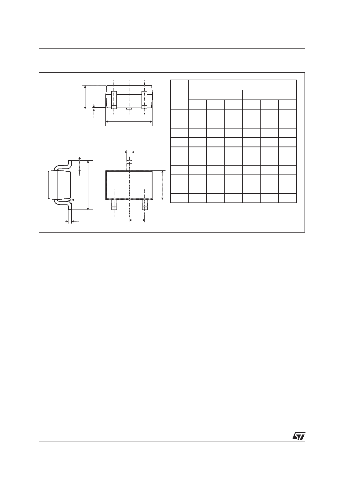
PACKAGE MECHANICAL DATA
SOT-323
A
A1
D
REF.
A 0.8 1.1 0.031 0.043
A1 0.0 0.1 0.0 0.004
b 0.25 0.4 0.010 0.016
c 0.1 0.26 0.004 0.010
b
L
D 1.8 2.0 2.2 0.071 0.079 0.086
E 1.15 1.25 1.35 0.045 0.049 0.053
e 0.65 0.026
H
θ
H 1.8 2.1 2.4 0.071 0.083 0.094
E
L 0.1 0.2 0.3 0.004 0.008 0.012
θ 030°030°
Millimeters Inches
Min. Typ. Max. Min. Typ. Max.
DIMENSIONS
c
e
4/5

PACKAGE MECHANICAL DATA
SOD-323
BAS70J / BAS70W / BAS70-04W /BAS70-05W / BAS70-06W
H
b
A1
REF.
Millimeters Inches
DIMENSIONS
Min. Max. Min. Max.
E
A 1.17 0.046
A1 0 0.1 0 0.004
D
A
b 0.25 0.44 0.01 0.017
c 0.1 0.25 0.004 0.01
c
Q1
D 1.52 1.8 0.06 0.071
E 1.11 1.45 0.044 0.057
H 2.3 2.7 0.09 0.106
L
L 0.1 0.46 0.004 0.02
Q1 0.1 0.41 0.004 0.016
Ordering type Marking Package Weight Base qty Delivery mode
BAS70W D28 SOT-323 0.006g 3000 Tape & reel
BAS70-04W D31 SOT-323 0.006g 3000 Tape & reel
BAS70-05W D30 SOT-323 0.006g 3000 Tape & reel
BAS70-06W D29 SOT-323 0.006g 3000 Tape & reel
BAS70J 76 SOD-323 0.005g 3000 Tape & reel
n Epoxy meets UL94,V0
Information furnished is believed to be accurate and reliable. However, STMicroelectronicsassumes noresponsibilityforthe consequences of
use of such information nor for any infringement of patents or other rights of third partieswhich mayresultfromits use.Nolicense is granted by
implication or otherwise under any patent or patent rights of STMicroelectronics. Specifications mentioned in this publication are subject to
change withoutnotice. This publication supersedes and replaces all information previouslysupplied.
STMicroelectronics products are not authorized for use as critical components in life support devices or systems without express written approval of STMicroelectronics.
The ST logo is a registered trademark of STMicroelectronics
2000 STMicroelectronics - Printed in Italy - All rights reserved.
STMicroelectronics GROUP OF COMPANIES
Australia - Brazil - China - Finland - France - Germany - Hong Kong - India - Italy - Japan - Malaysia
Malta - Morocco - Singapore - Spain - Sweden - Switzerland - United Kingdom - U.S.A.
http://www.st.com
5/5
 Loading...