

1/4
BAS70-07S / BAS70-08S
®
December 2001 - Ed: 2A
RF DETECTION DIODE
■
LOW DIODE CAPACITANCE
■
LOW SERIES INDUCTANCE AND RESISTANCE
■
SURFACE MOUNT PACKAGE
FEATURES AND BENEFITS
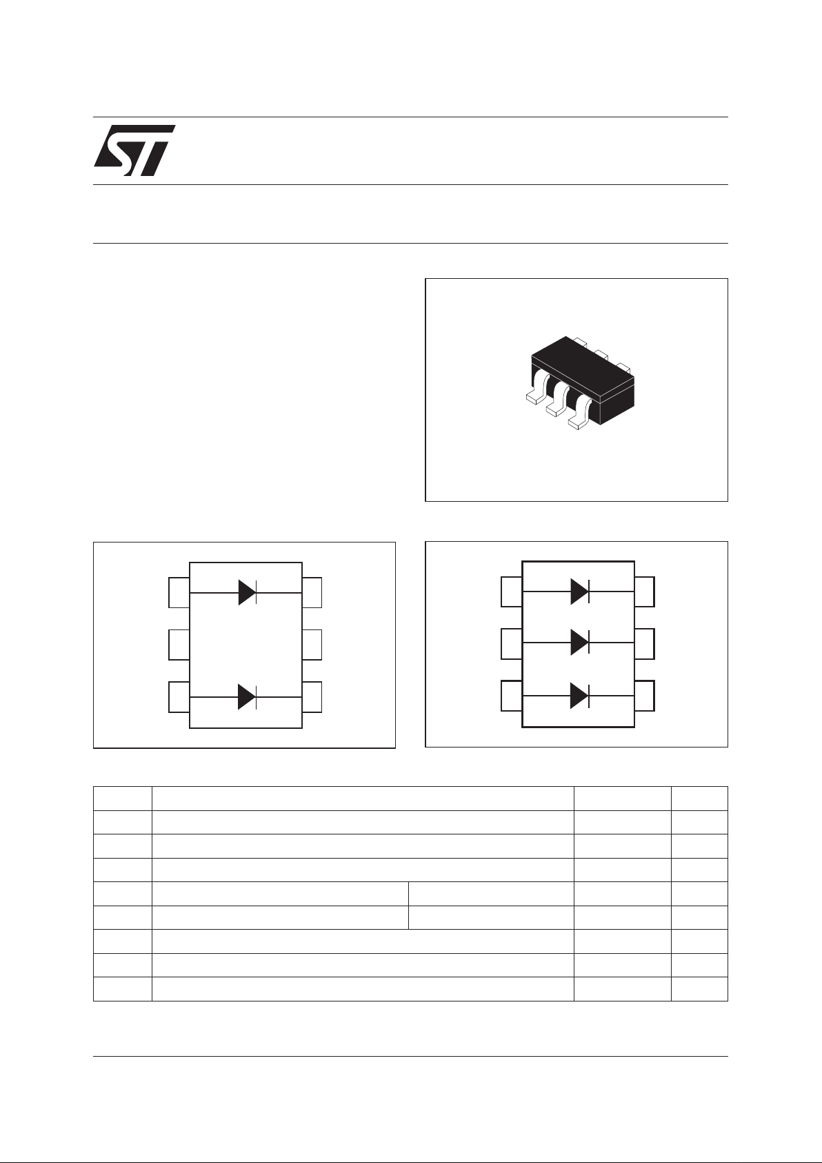
Dual and Triple Schottky diode in SOT323-6L
package. This diode is intented to be used in RF
application for signal detection and temperature
compensation.
DESCRIPTION
SOT323-6L
Symbol Parameter Value Unit
V
R
Continuous reverse voltage 70 V
I
F
Continuous forward current 70 mA
I
FRM
Repetitive peak forward current 70 mA
I
FSM
Surge non repetitive forward current tp= 10 ms sinusoidal 1 A
P Power Dissipation Ta = 55°C 250 mW
T
stg
Storage temperature range - 65 to +150 °C
Tj Maximum junction temperature 150 °C
TL Maximumtemperature for soldering 260 °C
ABSOLUTE RATINGS (limiting values)
1
2
3
6
5
4
BAS70-07S SCHEMATIC DIAGRAM
1
2
3
6
5
4
BAS70-08S SCHEMATIC DIAGRAM
BAS70-07S / BAS70-08S
2/4
Symbol Parameter Tests Conditions Min. Typ. Max. Unit
V
F
Forward voltage drop IF= 1 mA 0.41 V
I
F
= 10 mA 0.75 V
I
F
=15mA 1 V
I
R
Reverse leakage current VR=70V 10 µA
V
BR
Breakdown voltage IR=10µA 70 V
STATIC ELECTRICAL CHARACTERISTICS (Tj = 25°C otherwise specified)
Symbol Parameter Tests Conditions Min. Typ. Max. Unit
C Junction capacitance V
R
=0V F=1MHz 2 pF
R
F
Differential forward
resistance
IF= 10 mA F = 100 MHz 30 Ohm
L
s
Series inductance 1.5 nH
ELECTRICAL CHARACTERISTICS
Symbol Parameter Value Unit
R
th (j-a)
Junction to ambient on printed circuit board FR4
with recommended pad layout
500 °C/W
THERMAL RESISTANCE

BAS70-07S / BAS70-08S
3/4
1.E-01
1.E+00
1.E+01
1.E+02
0.0 0.2 0.4 0.6 0.8 1.0 1.2
VFM(V)
Tj=150°CTj=150°C
Tj=125°CTj=125°C
Tj=85°CTj=85°C
Tj=25°CTj=25°C
Tj=-40°CTj=-40°C
IFM(mA)
Fig. 1: Forward voltage drop versus forward
current (typical values).
1.E-03
1.E-02
1.E-01
1.E+00
1.E+01
1.E+02
0 10203040506070
IR(µA)
VR(V)
Tj = 150°C
Tj = 25°C
Tj = 85°C
Fig. 2: Reverse leakage current versus reverse
voltage applied (typical values).
10
100
1000
0.1 1.0 10.0
Rf( )Ω
IF(mA)
F = 10kHz
Tj = 25°C
Fig. 3: Differential forward resistance versus
forward current (typical values).
0.0
0.1
0.2
0.3
0.4
0.5
0.6
0.7
0.8
0.9
1.0
1.1
1.2
1.3
1.4
1.5
0 10203040506070
C(pF)
VR(V)
F = 1MHz
Vosc = 30mV
Tj = 25°C
RMS
Fig. 4: Junction capacitance versus reverse
voltage applied (typical values).
10.0
100.0
1000.0
1.E-02 1.E-01 1.E+00 1.E+01 1.E+02
Zth(j-a)(°C/W)
tp(s)
Fig. 5: Variation of thermal impedance junction to
ambient versus pulse duration (printed circuit
board, epoxy FR4).
300
350
400
450
500
550
600
0 5 10 15 20 25 30 35 40 45 50
Rth(j-a)
S(mm²)
Fig. 6: Thermal resistance junction to ambient
versus copper surface under each lead (printed
circuit board, epoxy FR4).

BAS70-07S / BAS70-08S
4/4
Informationfurnished is believed to be accurateand reliable. However, STMicroelectronics assumes noresponsibility for the consequences of
useof such information nor for anyinfringement of patents or other rights of third parties which may result from its use. No license is grantedby
implication or otherwise under any patent or patent rights of STMicroelectronics. Specifications mentioned in this publication are subject to
change without notice. This publication supersedes and replaces all information previously supplied.
STMicroelectronics products are not authorized for use as critical components in life support devices or systems without express written approval of STMicroelectronics.
The ST logo is a registered trademark of STMicroelectronics
© 2001 STMicroelectronics - Printed in Italy - All rights reserved.
STMicroelectronics GROUP OF COMPANIES
Australia - Brazil - Canada - China - Finland - France - Germany
Hong Kong - India - Israel - Italy - Japan - Malaysia - Malta - Morocco - Singapore
Spain - Sweden - Switzerland - United Kingdom - United States.
http://www.st.com
PACKAGE MECHANICAL DATA
SOT323-6L
A2
A
A1
E
b
HE
D
ee
Q1
c
0.3mm
1mm
1mm
0.35mm
2.9mm
FOOTPRINT DIMENSIONS (millimeters)
Type Marking Package Weight Base qty Delivery mode
BAS70-07S D32
SOT323-6L 0.006g 3000 Tape & reel
BAS70-08S D33
■
Epoxy meets UL94, V0
MARKING
REF.
DIMENSIONS
Millimeters Inches
Min. Max. Min. Max.
A 0.8 1.1 0.031 0.043
A1 0 0.1 0 0.004
A2 0.8 1 0.031 0.039
b 0.15 0.3 0.006 0.012
c 0.1 0.18 0.004 0.007
D 1.8 2.2 0.071 0.086
E 1.15 1.35 0.045 0.053
e 0.65Typ. 0.025 Typ.
HE 1.8 2.4 0.071 0.094
Q1 0.1 0.4 0.004 0.016
 Loading...