

Service manual
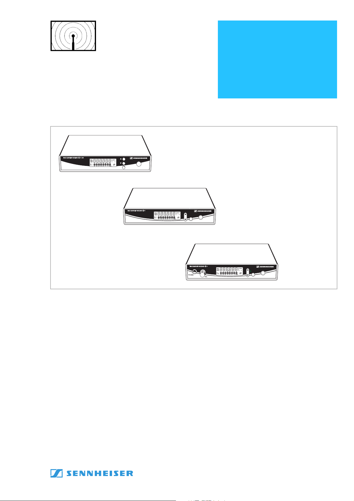
EM 100 G2
EM 300 G2
EM 500 G2
SA 040818
SET
POWER
300
EM 100 G2
ON
SET
EM 300 G2
500
SET
Short Description
The three stationary receivers EM 100 G2, EM 300 G2 and EM 500 G2
,True Diversity’ receivers and are equipped with the HDX noise reduction
are
system. Each receiver has a switching bandwidth of 36MHz in the UHF band.
ON
EM 500 G2
Features
• 1440 UHF frequencies available for interference-free reception.
• Direct channel selection via presets.
• Scan function for finding free receive channels.
• Low battery warning on transmitter and receiver.
• Squelch pilot tone for interference-free operation.
• Sound check mode for checking transmission conditions
(only EM 500 G2).
Subject to alterations
Sennheiser electronic GmbH & Co. KG • 30900 Wedemark
Phone: +49 (5130) 600 0 • Fax: +49 (5130) 600 300 1/32

Safety requirements
Observe safety regulations.
Observe ESD instructions while handling electrostatically endangered components.
Only skilled persons are allowed to alter and repair. For repairs and exchanges only
approved components according to the current spare parts list are allowed.
It is forbidden to alter the product unauthorised.
If not observed the adaptor is legally liable for possible results of damage.
repairs/exchanges The following instructions for overhaul and testing must be followed. In case of
unusual problems please contact your Sennheiser distributor.
EM 500 G2, EM 300 G2, EM 100 G2
2/32 08/2004

Table of contents
1 Controls and indicators .................................................................................4
2 Technical data................................................................................................. 5
2.1 General.................................................................................................................... 5
2.2 RF part..................................................................................................................... 5
2.3 AF part .................................................................................................................... 6
3 Description ...................................................................................................... 7
3.1 Mainboard .............................................................................................................. 7
3.2 RF module............................................................................................................... 8
3.3 Display module...................................................................................................... 9
3.4 Monitor module (only EM 500 G2).................................................................... 9
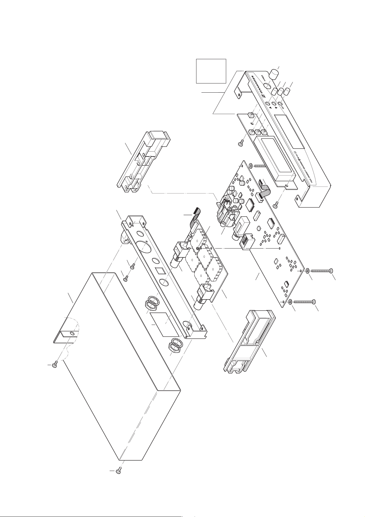
4 Exploded view...............................................................................................10
4.1 Exploded view: EM 100 G2................................................................................ 10
4.2 Exploded view: EM 300 G2, EM 500 G2 .......................................................... 11
5 Test and alignment instructions................................................................ 13
5.1 Measuring and test equipment .......................................................................13
5.2 Measuring set-up................................................................................................13
5.3 Test table..............................................................................................................14
5.4 Reading out/changing unit data via the “DATA“ service interface .........17
6 Circuit diagrams ...........................................................................................19
Block diagram ...................................................................................................................19
Mainboard, circuit diagram, part 1/3...........................................................................20
Mainboard, circuit diagram, part 2/3...........................................................................21
Mainboard, circuit diagram, part 3/3...........................................................................22
RF board, circuit diagram, part 1/3..............................................................................23
RF board, circuit diagram, part 2/3..............................................................................24
RF board, circuit diagram, part 3/3..............................................................................25
Monitoring module MOD.A020, circuit diagram........................................................26
Interconnector assignmet ..............................................................................................27
Mainboard, component side ..........................................................................................28
Mainboard, solder side....................................................................................................29
RF board, component side..............................................................................................30
RF board, solder side .......................................................................................................31
Monitoring module: MOD.A020, component side .....................................................32
Monitoring module: MOD.A020, solder side...............................................................32
EM 500 G2, EM 300 G2, EM 100 G2
3/32 08/2004
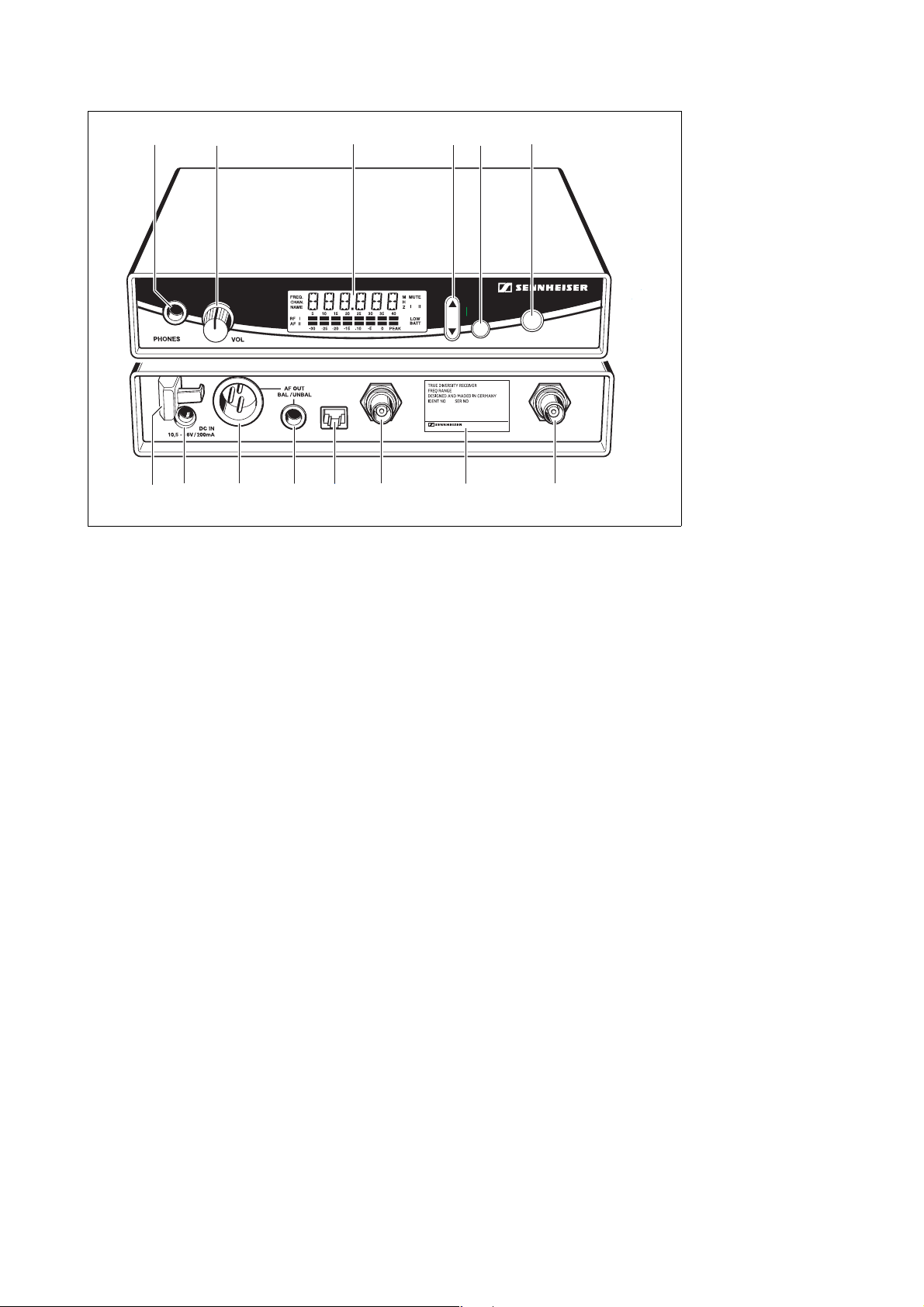
1 Controls and indicators
Front
쐃 Headphone output, ¼
(only EM 500 G2)
SET
DATA
쐅쐈 쐉 씈 씉
"
(6.3mm) jack socket (PHONES)
ON
쐇 Headphone volume control (VOL)
(only EM 500 G2)
쐋 Display
쐏 Button /
(two separate buttons on EM 100 G2)
쐄 Button SET
쐂 Button ON / POWER
Back panel
쐆 Cable grip for mains unit connector cable
쐊 DC socket for power supply unit connection (DC IN)
쐎 XLR socket for AF output (AF OUT BAL)
쐅 Audio output jack socket (AF OUT UNBAL)
쐈 RJ45 socket as service interface (DATA)
쐉 BNC socket as antenna input 2 (ANT II)
씈 Type plate
씉 BNC socket, antenna input 1 (ANT I)
EM 100 G2, EM 300 G2, EM 500 G2
08/2004 4/32

2 Technical data
2.1 General
Nominal output ______________________ +12V
Operating voltage ____________________ +10.5 ... +16V
Current consumption at nominal voltage ___ typ. 200mA
Quiescent current consumption (standby) __ typ. 50mA
Temperature range ___________________ -10°C ... +55°C
Dimensions (in mm)___________________ 212 x 145 x 38
Weight: ____________________________ approx. 1200g
Approval ___________________________ D801 488L RF
Max. audio output level (balanced/unbalanced)
3-pin XLR socket_________________ +19dBu
1/4 " (6.3 mm) jack socket_________ +13dBu
Headphone output (only EM 500 G2)
THD (at nominal deviation, 1 kHz)
Control range (only EM 500 G2) _________ 40dB
_____¼
__________ ≤ 0.9%
DC
"
(6.3 mm) jack socket, stereo
2.2 RF part
Receiver principle _____________________ true diversity
Frequency ranges_____________________ 518 – 554MHz
626 – 662MHz
740 – 776MHz
786 – 822MHz
830 – 866MHz
Switching bandwidth __________________ 36MHz
Receive frequencies ___________________ 1440
Channel separation ___________________ > 400kHz
Channel grid_________________________ 25kHz
1. Oscillator frequency _________________ f
1. Intermediate frequency ______________ 241MHz
2. Oscillator frequency _________________ 230.3MHz
2. Intermediate frequency ______________ 10.7MHz
Modulation__________________________ wideband FM
Nominal/peak deviation________________ ±24kHz / ±48kHz
Frequency stability
Adjacent channel selection
EM 100 G2 _____________________
EM 300 G2
EM 500 G2
Intermodulation attenuation
EM 100 G2 _____________________
EM 300 G2
EM 500 G2
________________________ ≤ ±15ppm
__________________________ ≥ 68dB
__________________________ ≥ 70dB
__________________________ ≥ 68dB
__________________________ ≥ 70dB
= fe + 241MHz
Osc
≥ 65dB
≥ 65dB
EM 100 G2, EM 300 G2, EM 500 G2
5 08/2004

Blocking
EM 100 G2, EM 300 G2
EM 500 G2
Squelch _____________________________off, low: 5dBµV,
Squelch pilot tone _____________________adjustable
S/N = 52 dBA (unweighted with HDX) _____< 2.5µV (typ. 1.4µV)
S/N = 80 dB (unweighted with HDX) _______< 10µV (typ. 6µV)
S/N max (peak deviation with HDX) _______> 120dB(A) (typ. 124dB(A)
Antenna inputs ______________________RF input: 2 BNC sockets, 50
_________________________ ≥ 75dB
______________ ≥ 70dB
mid: 15dBµV
high: 25dBµV
2.3 AF part
Compander system ____________________HDX
S/N (AF OUT)
EM 100 G2
EM 300 G2
EM 500 G2
AF output voltage (nominal deviation)
Unbalanced _____________________1.25V = +4dBu
Balanced _______________________2.45V = +10dBu
AF output voltage (peak deviation)
Unbalanced 3.4V = +13dBu
Balanced 6.8V = +19dBu
AF frequency response _________________50Hz ... 18kHz; -3dB
Monitor output level/load _______________> 100mW/32
AF outputs ______________________¼" (6.3mm) jack socket
Pilot tone
Pilot tone frequency ______________32.768kHz
Pilot tone deviation _______________
_____________________ ≥ 110dB(A)
_____________________ ≥ 112dB(A)
_____________________ ≥ 115dB(A)
Ω (only EM 500 G2)
Unbalanced
XLR-3M, balanced
≥ 1.5kHz
Ω
EM 100 G2, EM 300 G2, EM 500 G2
08/2004 6/32

3 Description
The receiver has a modular structure and comprises the following boards:
• Mainboard
• Display module
• RF module
• Monitor module (only EM 500 G2)
The display, RF and monitor modules are each connected to the mainboard via a
15-pin ribbon connection. The following sections explain the principal functions.
3.1 Mainboard
The mainboard is a single-sided PCB assembly. It is manually screwed to the side
walls, the front and the back panel wall and the RF module. The mainboard
performs the following functions:
• Conditioning of power supply
• Conditioning of AF signals
• Provision of power supply to additional modules
• Control of own functions and the RF and monitor module via the
microprocessor
3.1.1 Processing the diversity signal
The signal from the RF module with the highest field strength is switched by the
U50 or U51 diversity switches and reaches four signal conditioning blocks that are
connected in parallel.
3.1.2 U52 squelch switch with AF conditioning
If the squelch threshold you set is exceeded, U1 uses U52 to switch the AF signal
and activates the AF high pass filter with U75-1, the AF low pass filter with U75-2
and U76-1, the HDX expander with U100 and the AF stages U101-1, U101-2 and
U76-2.
With EM 500 G2 the AF stages U101-1 and U101-2 are used via analog switch U300
as LOW-CUT filters with a threshold frequency of 200Hz and with U301 as
HI-BOOST filters with an increase of approx. 5dB at 10kHz. Control is via U1,
Q300-1 and Q300-2.
The peak detector is connected to the level indicator behind U76-1 with U100 operational amplifiers (U100-2 and U100-1) whose output signal DEV_L is available to
microprocessor U1 for evaluation.
The two AF signals AF_0 (U76-2) and AF_180 (U101-2) both reach a divider
resistance chain at the inputs of analog switches U175 and U176, via which eight
AF signal switching stages are set by the user. The structure is strictly balanced and
is laid behind the active stages to guarantee full signal to noise ratio even if the
AF signal is weakened by approx. 40dB. From the two outputs, the AF signal then
reaches across various components to protect from ESD parasitic signals and
phantom voltage at AF sockets P175 and J175.
EM 100 G2, EM 300 G2, EM 500 G2
7 08/2004

3.1.3 Evaluation of the TX battery signal
The battery telegram sent by the transmitter reaches the U60-2 trigger stage, at
whose output appropriate square wave signals are available for evaluation by U1,
via the 4Hz low pass filter with U60-1.
3.1.4 Evaluation of the pilot signal
The 32.768kHz pilot signal sent by the transmitter is filtered from the signal mix
by the active crystal filter with Q95, Y95 and U95-1, rectified via the D95 diode and
made available for evaluation by U1 via trigger stage U96-1.
3.1.5 Functions of microprocessor U1
The receiver is controlled by the 8-bit U1 microprocessor, which contains in its flash
memory the control program and uses a sub-area as an EEPROM for saving data
even in the event of power failure. The microprocessor uses a 4MHz crystal to
generate both its own internal 8MHz cycle and the reference frequency for the
RF module PLL. It processes the signals already described in line with the program
specifications and the user specifications that can be set on an individual basis via
a menu.
3.1.6 Service interface (RJ45 socket)
The service interface “DATA“ with RS485 protocol, located on the back panel of the
unit, fulfills an important function. The RJ45 socket allows the relevant EEPROM parameters on the RF module and the simulated EEPROM to be read out and modified
in the microprocessor. This interface also enables a software update as part of the
hardware options. For example, the RJ45 socket enables you to read unit data and
write-in after replacing a board. The necessary service software is
available for download free of charge on our Internet homepage:
www.sennheiser.com > Service & Distributors > Service Documentation >
Download
3.2 RF module
The RF module is a single-sided PCB assembly that is fixed to the back panel via the
BNC input sockets and to the mainboard via a sheet metal brace. The RF module
performs RF conditioning until demodulation of the IF signal. The module is connected to the mainboard via a 15-pin ribbon connection; the following functions are
performed by the plug-in connection:
• Incoming power supply of 5V DC from the mainboard.
• Incoming system cycle (4MHz) from mainboard microprocessor.
• 2 x outgoing AF voltage to mainboard
• 2 x RSSI voltage to mainboard.
• Communication between the mainboard microprocessor and
the EEPROM or the PLL for the RF module.
EM 100 G2, EM 300 G2, EM 500 G2
08/2004 8/32

3.2.1 RF module shielded compartments
The shielded compartments on the RF module perform the following functions:
• The two compartments between the BNC sockets contain the second mixer,
the 10.7MHz limiting amplifier and the FM demodulator.
• The compartment directly behind the BNC socket contains RF conditioning
up to an including the SAW filter for the first IF.
• The middle compartment performs frequency conditioning for the first
oscillator with VCO, buffer and PLL for both diversity channels.
The input filters are assembled outside the shielded compartments to ensure that
parasitic LO frequency currents cannot be coupled directly to the RF input. The input filters are relatively complex owing to the integrated IF and LO cases,
but nevertheless do not require alignment.
3.2.2 Alignment of the RF module
The only components still to be adjusted are
• C540 for alignment of VCO voltage at center frequency,
• C330 for setting the LO2 crystal oscillator,
• The L310 and L410 discriminator coils, and
• The two level adjusters for the AF outputs.
For communication with the processor on the mainboard, the RF module contains
the U700 EEPROM, in which the relevant frequency range data, the RSSI table and
other status data are stored. Communication is processed via the same bus used by
the microprocessor to communicate with the PLL U500 (frequency setting).
3.3 Display module
The display module for the status displays is connected to the mainboard via a
15-pin ribbon connection.
3.4 Monitor module (only EM 500 G2)
The monitor module (MOD.A020) is a single-sided PCB assembly and is connected
to the mainboard via a 15-pin plug-in connector. The monitor module PCB has a jack
socket for connecting headphones, and an appropriate volume control. The monitor
module also has a complete U1 and U2 amplifier for each AF phase; the volume can
be adjusted via R1.
The monitor module is primarily intended for stereo operation, but in phase configuration is possible for mono operation. If you want to minimize the volume differences in mono operation between the left and right channel (this may occur as a
result of the tolerances of R1), you must close the M1 solder bridge.
You must not close the M1 solder bridge if you are using the monitor
module in stereo mode.
EM 100 G2, EM 300 G2, EM 500 G2
9 08/2004
4 Exploded view
4.1 Exploded view: EM 100 G2
003
007
*
*
006
incl.:
Pos. 006
017
018
013
017
018
018
018
002
001
020
020
008
013
016
016
012
019
011
009
003
005
005
004
004
002
EM 100 G2, EM 300 G2, EM 500 G2
08/2004 10/32
 Loading...