

Page 1
1. OUTLINE OF CIRCUIT DESCRIPTION
1-1. CA1 and A PART OF CA2 CIRCUIT
DESCRIPTIONS
Around CCD block
1. IC Configuration
CA1 board
IC901 (ICX411AQ) CCD imager
CA2 board
IC931 H driver, CDS, AGC and A/D converter
IC934 (CXD3400N) V driver
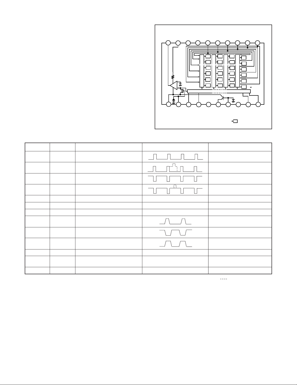
2. IC901 (CCD imager)
[Structure]
Interline type CCD image sensor
Image size Diagonal 8.293 mm (1/1.8 type)
Pixels in total 2384 (H) x 1734 (V)
Recording pixels 2288 (H) x 1712 (V)
10
11
1B
OUT
V
DD
V
9
12
GND
RG
Ø
TEST
8
13
2
Ø
H
Ø
V
TEST
7
6
Ye
G
Ye
G
Ye
Vertical register
G
Horizontal register
15
14
1
Ø
GND
H
Fig. 1-2. CCD Block Diagram
1A
Ø
Ø
V
V
4
5
Cy
Ye
Mg
G
Cy
Ye
Mg
G
Cy
Ye
Mg
G
17
16
SUB
SUB
C
Ø
(Note) : Photo sensor
3
18
Ø
V
L
V
Cy
Mg
Cy
Mg
Cy
Mg
19
2
3A
Ø
V
1
Ø
H
3B
2
1
(Note)
20
4
Ø
V
2
Ø
H
Pin No.
1
2, 3
4
5, 6
9, 15
10
11
12
13, 20
14, 19
16
17
18
Symbol
4
Vø
Vø
3A, Vø3B
Vø2
Vø1A, Vø1B
GND
OUT
V
VDD
øRG
Hø2
Hø
1
øSUB
CSUB
VL
Pin Description
Vertical register transfer clock
Vertical register transfer clock
Vertical register transfer clock
Vertical register transfer clock
GND
Signal output
Circuit power
Reset gate clock
Horizontal register transfer clock
Horizontal register transfer clock
Substrate clock
Substrate bias
Protection transistor bias
Table 1-1. CCD Pin Description
Waveform
GND
DC
DC
DC
DC
Voltage
-7.5 V, 0 V
-7.5 V, 0 V, 15 V
-7.5 V, 0 V
-7.5 V, 0 V, 15 V
0 V
Aprox. 10 V
15 V
12.5 V, 16 V
0 V, 5 V
0 V, 5 V
Approx. 8 V
Approx. 8 V
(Different from every CCD)
When sensor read-out
– 2 –
Page 2
3. IC934 (V Driver) and IC931 (H Driver)
An H driver and V driver are necessary in order to generate
the clocks (vertical transfer clock, horizontal transfer clock
and electronic shutter clock) which driver the CCD. IC934 is
V driver. In addition the XV1-XV4 signals which are output
from IC102 are the vertical transfer clocks, and the XSG signal which is output from IC102 is superimposed onto XV1
and XV3 at IC934 in order to generate a ternary pulse. In
addition, the XSUB signal which is output from IC102 is used
as the sweep pulse for the electronic shutter. A H driver is
inside IC931, and H1, H2 and RG clock are generated at
IC931.
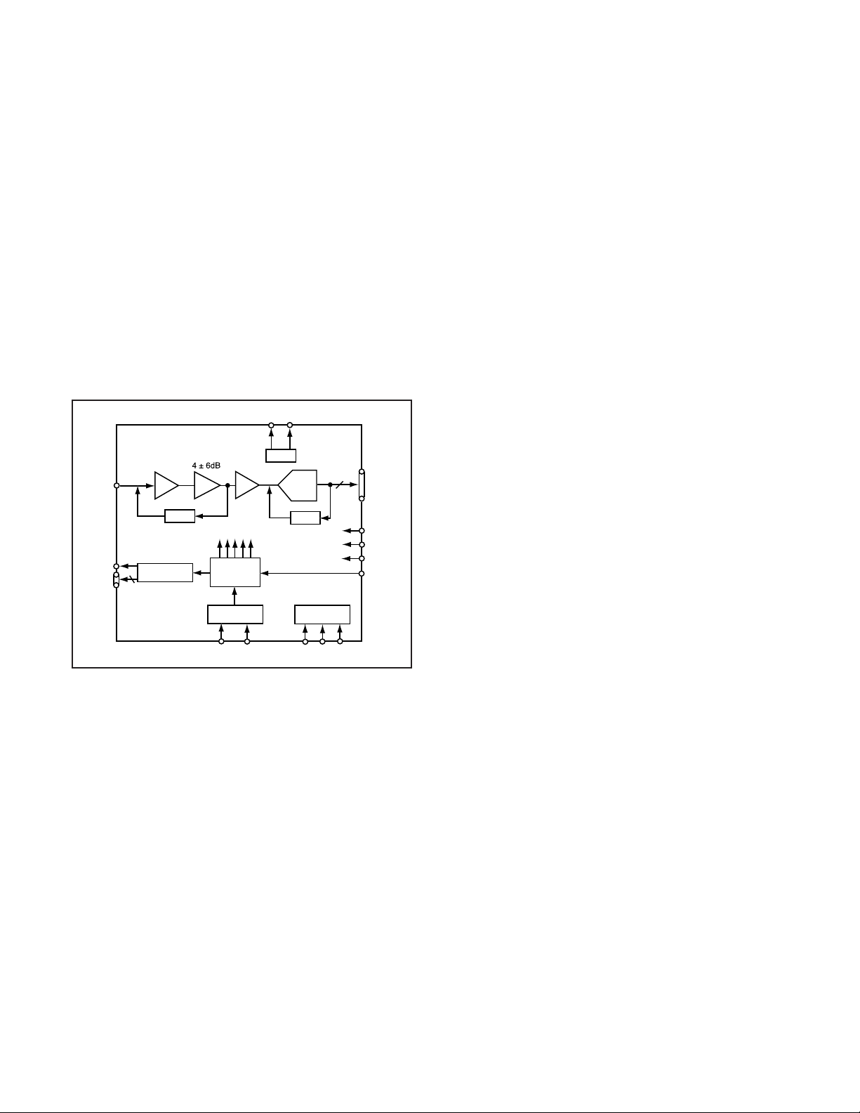
4. IC931 (CDS, AGC Circuit and A/D Converter)
The video signal which is output from the CCD is input to Pin
(29) of IC931. There are inside the sampling hold block, AGC
block and A/D converter block.
The setting of sampling phase and AGC amplifier is carried
out by serial data at Pin (37) of IC911. The video signal is
carried out A/D converter, and is output by 12-bit.
VRB
VRT
VREF
CCDIN
CDS
PxGA
2~36 dB
VGA
ADC
12
DOUT
RG
H1-H4
HORIZONTAL
4
DRIVERS
CLAMP
INTERNAL
CLOCKS
PRECISION
TIMING
CORE
SYNC
GENERATOR
VD
HD
Fig. 1-2. IC931 Block Diagram
CLAMP
INTERNAL
REGISTERS
SL
SCK
CLPOB
CLPDM
PBLK
CLI
SDATA
– 3 –
Page 3

1-2. CA2 CIRCUIT DESCRIPTION
1. Circuit Description
1-1. Digital clamp
The optical black section of the CCD extracts averaged values from the subsequent data to make the black level of the
CCD output data uniform for each line. The optical black section of the CCD averaged value for each line is taken as the
sum of the value for the previous line multiplied by the coefficient k and the value for the current line multiplied by the
coefficient 1-k.
1-2. Signal processor
1. γ correction circuit
This circuit performs (gamma) correction in order to maintain
a linear relationship between the light input to the camera
and the light output from the picture screen.
2. Color generation circuit
This circuit converts the CCD data into RGB signals.
3. Matrix circuit
This circuit generates the Y signals, R-Y signals and B-Y signals from the RGB signals.
4. Horizontal and vertical aperture circuit
This circuit is used gemerate the aperture signal.
1-3. AE/AWB and AF computing circuit
The AE/AWB carries out computation based on a 64-segment
screen, and the AF carries out computations based on a 6segment screen.
1-4. SDRAM controller
This circuit outputs address, RAS, CAS and AS data for controlling the SDRAM. It also refreshes the SDRAM.
1-5. Communication control
1. SIO
This is the interface for the 8-bit microprocessor.
2. PIO/PWM/SIO for LCD
8-bit parallel input and output makes it possible to switch between individual input/output and PWM input/output.
1-6. TG/SG
Timing generated for 4 million pixel CCD control.
1-7. Digital encorder
It generates chroma signal from color difference signal.
2. Outline of Operation
When the shutter opens, the reset signals (ASIC and CPU)
and the serial signals (“take a picture” commands) from the
8-bit microprocessor are input and operation starts.
When the TG/SG drives the CCD, picture data passes through
the A/D and CDS, and is then input to the ASIC as 12-bit
data. The AF, AE, AWB, shutter, and AGC value are computed from this data, and three exposures are made to obtain
the optimum picture. The data which has already been stored
in the SDRAM is read by the CPU and color generation is
carried out. Each pixel is interpolated from the surrounding
data as being either Ye, Cy, Mg or B primary color data to
produce R, G and B data. At this time, correction of the lens
distortion which is a characteristic of wide-angle lenses is
carried out. After AWB and γ processing are carried out, a
matrix is generated and aperture correction is carried out for
the Y signal, and the data is then compressed by JPEG and
is then written to card memory (smart media).
When the data is to be output to an external device, it is taken
data from the memory and output via the USART. When played
back on the LCD and monitor, data is transferred from memery
to the SDRAM, and the image is then elongated so that it is
displayed over the SDRAM display area.
3. LCD Block
During monitoring, YUV conversion is carried out for the 12bit CCD data which is input from the A/D conversion block to
the ASIC and is then transferred to the DRAM so that the
CCD data can be displayed on the LCD.
The data which has accumulated in the DRAM is passed
through the NTSC encoder , and after D/A conversion is carried out to change the data into a Y/U/V signal, the data is
sent to the LCD panel and displayed.
If the shutter button is pressed in this condition, the 12-bit
data which is output from the A/D conversion block of the
CCD is sent to the DRAM (DMA transfer), and after processor, it is displayed on the LCD as a freeze-frame image.
During playback, the JPEG image data which has accumulated in the flash memory is converted to YUV signals, and
then in the same way as during monitoring, it is passed through
the NTSC endoder, and after D/A conversion is carried out to
change the data into a Y/U/V signal, the data is sent to the
LCD panel and displayed.
The three analog signals (Y/U/V signals) from the ASIC are
converted into RGB signals by the LCD driver, and these RGB
signals and the control signal which is output by the LCD driver
are used to drive the LCD panel. The RGB signals are 1H
transposed so that no DC component is present in the LCD
element, and the two horizontal shift register clocks drive the
horizontal shift registers inside the LCD panel so that the 1H
transposed RGB signals are applied to the LCD panel. Because the LCD closes more as the difference in potential between the COM (common polar voltage: fixed at DC) and the
R, G and B signals becomes greater, the display becomes
darker; if the difference in potential is smaller, the element
opens and the LCD become brighter.
– 4 –
Page 4

1-3. PW1 POWER CIRCUIT and LENS DRIVE
BLOCK DESCRIPTION
1. Outline
This is the main power circuit, and is comprised of the following blocks.
Switching power controller (IC501)
Analog system power output (Q5001, T5001)
Digital 1.8 V power output (Q5009, L5008)
Digital 3.3 V power output (Q5010, L5009)
Digital 3.3 V step-up power output (Q5011, L5010)
LED backlight power output (Q5012, L5011)
5 V and LCD system power output (Q5015, L5012)
2. Switching Controller
This is the basic circuit which is necessary for controlling the
power supply for a PWM-type switching regulator, and is provided with six built-in channels, only CH1 (analog system
power output), CH2 (digital 1.85 V system power output), CH3
(digital 3.35 V system power output), CH4 (digital 3.35 V stepup power output), CH5 (LED back light power output) and
CH6 (5 V and LCD system power output) are used. Feedback
from 15.0 V (A) (CH1), 1.8 V (D) (CH2), 3.3 V (D) (CH3), 4.7
V (L) (CH4), LED backlight output (CH5) and 5 V (CH6) power
supply outputs are received, and the PWM duty is varied so
that each one is maintained at the correct voltage setting level.
7. LED Backlight Power Output
A constant current flows to the backlight LEDs. Feedback for
the voltage of R5098 is provided to the power controller (Pin
(2) of IC501) so that PWM control can be carried out.
8. 5 V and LCD System Power Output
5 V is output. Feedback for the 5 V is provided to the swiching
controller (Pin (4) of IC501) so that PWM control can be carried out. And also this CH6 pulse is carried out voltage doubler so that 9.9 V (L) for LCD is output.
9. Lens drive block
9-1. Iris drive
When the drive signals (IRIS_A, IRIS_/A, IRIS_B and IRIS_/
B) which are output from the ASIC expansion port (IC105), the
stepping motor is driven by the driver (IC951), and are then
used to drive the iris steps.
9-2. Focus drive
When the drive signals (FIN_A, FIN_-A, FIN_B and FIN_-B)
which are output from the ASIC expansion port (IC106), the
focus stepping motor is driven by the driver (IC951). Detection
of the standard focusing positions is carried out by means of
the photointerruptor (FOCUS PI) inside the lens block.
2-1. Short-circuit Protection
If output is short-circuited for the length of time determined
by the condenser which is connected to Pin (37) of IC501, all
output is turned off. The control signal (P ON) are recontrolled
to restore output.
3. Analog System Power Output
15.0 V (A) and -7.5 V (A) are output. Feedback for the 15.0 V
(A) is provided to the switching controller (Pin (40) of IC501)
so that PWM control can be carried out.
4. Digital 1.8 V Power Output
1.8 V (D) is output. Feedback for the 1.8 V (D) is provided to
the switching controller (Pins (43) of IC501) so that PWM
control can be carried out.
5. Digital 3.3 V Power Output
3.3 V (D) is output. Feedback for the 3.3 V (D) is provided to
the swiching controller (Pin (45) of IC501) so that PWM control can be carried out.
6. Digital 3.3 V Step-up Power Output
4.7 V is output. Feedback for the 4.7 V is provided to the
swiching controller (Pin (47) of IC501) so that PWM control
can be carried out.
9-3. Iris drive
The zoom DC motor drive signals (ZIN_A and ZIN_-A) which
are output from the ASIC are used to drive by the motor driver
(IC951). Detection of the zoom positions is carried out by means
of photointerruptor (ZOOM PI) inside the lens block.
9-4. Shutter drive
It is driven regular current with the motor driver IC (IC951) by
the shutter drive signals (SHUT_A and SHUT_/A) which are
output from the ASIC expansion port (IC106).
– 5 –
 Loading...