

Page 1

Part No. SKP20378 C3MSW/MWW
COLOUR TELEVISION
EE
EE
CC
CC8888----
AA
AA
SERVICE
REF.NO.
Model
Number:
CHASSIS
SERIES
VMC-7314P-00
VMC-7314E-00
VMC-7314P
VMC-7314E
The service Precaution:
The area enclosed by this line
( ) is directly connected with
AC mains voltage. When servicing the
area, connect an isolating transformer
between TV receiver and AC line to
eliminate hazard of electric shock.
Product safety notice:
Product safety should be considered
when a component replacement is
made in any area of a receiver.
Components indicated by a mark /!\ in
this circuit diagram show components
whose values have special significance to product safety. It is particularly recommended that only parts
specified on the part service manual
be used for components replacement
pointed out by the mark.
Circuit diagram notes :
1. All resistance values are in ohms,
K=1,000, M=1,000,000.
2. All resistance rated wattages are 1/6W
unless otherwise noted.
3. Excepting electrolytic capacitors, all
capacitance values of less than 1 are
expressed in µF and more than 1 are pF.
4. All capacitance rated voltages are 50V
unless otherwise noted.
5. All inductance values are in µH.
6. Voltage readings taken a digital voltmeter
are from point indicated chassis ground.
Voltage readings taken by using a colour
bar signal are with all controls at normal
position. Some voltages may vary with
signal strength.
7. Waveforms were taken with colour bar
and controls adjusted for normal picture.
Waveforms were taken by using a wide
band oscilloscope and a low capacity
probe.
DY1
X
L901
L81B28400
W901
1AV4W10
B00CWA
C501
35EM470
D501
ERA15-02
:EM01Z
J
L501
35EM220
C502
J30B
0250N
KDY-6
KDY-5
J30B
0250N
J30B
0250N
KDY-3
KDY-1
J30B
0250N
25KZ
0.1GQF
C807
KK4700
GQ
C816
KK4700
GQ
C818
L2B95
R6KN
L803
KK2200
GQ
C822
1/16GJ
15KC
R842
R838
1/16GJ
5.6KC
C817
CJ22
CGQ
CJ22
CGQ
C819
1/16GJ
5.6KC
R839
D826
MTZJ3.6B
:RD3.6EB2
R863
1/16GJ
15KC
R861
1/16GJ
330C
R862
1/16GJ
8.2KC
R815
1/16GJ100C
R831
10K
R845
1/16GJ220C
R844
1/16GJ220C
R843
1/16GJ220C
D831
1SS133
1/16GJ
2.7KC
R846
X801
EX0046
XC
L805
L2B9
5R6KN
C832
10EM47
C831
25KZ
0.1GQF
C834
CJ27
CGQ
C833
CJ27
CGQ
R808
1/16GJ
100C
R803
X
1/16G
J39KC
R880
1/16G
J10KC
R873
R872
1/16GJ
10KC
R875
1/16GJ470C
1/16GJ470C
R874
R832
10K
Q804
AH
AH
Q805
R840
1K
1/16GJ
10KC
R855
R856
1/16GJ
4.7KC
C814
KK3300GQ
+9V
R854
1/16GJ
4.7KC
R852
1/16GJ
27KC
22K
R853
L
( )L/L’
V OUT
IC501-1
1AA2HEF0
111--
MUTE
LED2
POWER
IGNOA
KEY IN
RC IN 8PIN(SC1)
PROTECT
SCL
SDA
FB-OUT
B-OUT
G-OUT
R-OUT
V-SYNC
H-SYNC
VDDA
PXFM
RESET
MCFM
TXCF
AVDD2TEST0
CVBS2
CVBS1
OSCOUT
OSCIN
VDDM
C810
16KK0.22
BA
R512A
1SJ220
R881
1K
1
PRO
TECT
1/16GJ
10KC
R1910
X
SW1904
1/16GJ6.8KC
R1904
1/16GJ
4.7KC
R1903
S10B1130N
SW1903
1/16GJ
8.2KC
R1902
1/16GJ
15KC
R1901
S10B1130N
SW1902
S10B1130N
SW1901
U20B20900
A1901
IC501
1
2
3
4
5
6
7
LA7832
C503
CJ39
CGQ
IC803
X24C04P:
24LC04B/P
1
2
3
45
6
7
8
C801
KZ0.01
GQF
L801
L2B95R6KN
R1907
820
Q1902
AH
L551
J
C835
KK4700GQ
R501
1/16GJ
1.8KC
KCP
J10AN050N
R1917
1/16GJ
390C
D1901
DLXRB0001653C
C1900
6.3EM100S
1
43
2
PC123F2
D615
24V
35EM470T
C643
25EM
1000
(T:DT)
C644
16EM1000
C645
12V
DJ82K
R635
1/16GJ
4.7KC
R636
RD6.8EB1
:MTZJ6.8A
D641
DJ
150K
R637
R625
2SJ39
Q613
2SD1710
YB
R624
2SJ68
R628
1/2CK
5.6MXG
R629
1/2CK
5.6MXG
C621
400KM1000XH:
400KM1000XS
C617
FK0.022
(BE:D)
Q612
2SC3807
RYA
C615
FJ0.012
(BE:D)
R626
DG
2.7K
R619
DJ220
C614
FK0.039
(BE:D)
R622
DJ15K
R621
1/2DJ
120K
R620
1/2DJ
120K
R615
DJ22K
D617
ES1:
ES1Z:
ED0448
D616
1S1553:
1S2076A
R617
2.2K
C606
1000KK1000
(CBB:HB)
Q611
QT0379(A:B):
2SA608(ECNP:
FCNP:GCNP:NFNPAN)
R611
5.6K
C601
250GM0.1XBC:
250HM0.1XD:
250MK0.1VA
ES(1:1Z):
D633
RU3M
D634
1000KK470
(NH:CRD)
C631
RD8.2EB1
:MTZJ8.2A
D619
D618
D614
400EM
100(XF:XS)
C607
5.6K
R623
RM11C:
ERC05-10B
D606D604
D603 D605
D649
1S1555:
ED0274
R638
1/2DJ
27K
R639
12K
R651
DJ10K
Q651
2SB985(S:T):
2SA1707(S:T)
R652
DJ3.9K
Q686
AJ
R689
1/16GJ22KC
R688
1/16GJ
10KC
Q685
AH
D685
RD6.8EB1
:MTZJ6.8A
C685
EM1
R687
1/16GJ
560KC
R686
DJ220K
115V
Q682
AH
C691
10EM100
5V
Q631
AH
J
L610
2400010
Q613H3
2400010
Q613H2
2400010
Q613H1
2400010
Q613H4
2400010
Q613H5
2400010
Q613H6
5WK3.9
(K:V)
R602
R3D6222NJ:
R30132XM<B-2.2K;2K>
VR641
R643
J
DJ10K
R642
2400030
T611H11
2400030
T611H8
2400030
T611H2
2400010
C607H2
2400010
C607H1
1S1555:
ED0274
D683
D631
EU2A
D635
EU2(:Z):
ED0277
L631
J
J
L633
L635
J
J
L634
T611H5
2400030
F601-A2
J20B00100:
J3EZ0333-
F601-A1
2400030
T611H17
L51B3840N
T611
5
8
2
3
11
12
13
14
15
16
17
SW601
S10B5230N
SW601-H1
2400010
2400010
SW601-H4
SW601-H2
2400010
2400010
SW601-H3
KAC-2
J30B0250N
J30B0250N
KAC-1
J30B0250N
KE-1
KE-2
J30B0250N
10EM1000
C663
+9V
C662
10EM220
DJ1.2K
R663
D669
1SS133
R661
DJ10K
Z20103---
L607
L608
Z20103---
BA178M09T:
UPC78M09AHF
321
IC661
2SB764E
Q661
L615
Z21B0040N
1SS133
D644
1SS133
D643
C641
160EM100X
F35B0840N
L601
2400030
L601H1
L601H2
2400030 2400030
L601H3
L601H4
2400030
2400010
R602H3
R602H2
2400010
2000KK
680(NH:
CRD)
C616
1SJ56
R666
Q613H
1AA2HE
A0110--
D603/.../D606
1
2
1
2
D614/D616/D618
+5V
C673
10EM100
1SS133
D671
10EM220
C672
IC671
123
BA178M05T:
UPC78M05AHF
IC801
1
2
3
4
5
6
7
8
9
10
11
12
13
14
15
16
17
18
19
20
21
22
23
24
QXXAVB759
25
26
27
28 29
30
31
32
33
34
35
36
37
38
39
40
41
42
43
44
45
46
47
48
49
50
51
52
53
54
55
56
C812
25KZ0.1
GQF
C811
16EM10
STATUS
ACK
AVDD3
SCL
SDA
Q802
AJ
IFAGC
RFAGC
C828
1/16GZ0C
PS601A
DHXAAEV0060:
JS601
J
C827
EM1
JS691
J
R672
2SJ15
F601
4A250VT
CSL
JS810
1/16GZ0C
R601
1/2DJ
220K
Q666
QT0378B
R667
560
C666
16EM47
D666
MTZJ5.6B
:RD5.6EB2
250GM0.1XBC:
250HM0.1XD:
250MK0.1VA
C602
C682
16EM33
R681
1/16GJ47KC
R645
1/2DJ4.7
R1900
1/16GJ56KC
R834
1/16GJ100C
R833
1/16GJ100C
R849
1/16GJ
2.7KC
R848
1/16GJ
2.7KC
R847
1/16GJ
2.7KC
R857
1/16GJ
33KC
R684
1/16GJ
10KC
R683
1/16GJ
33KC
Q681
AH
C433
16EM47
R696
1/16GJ
22KC
R697
1/16GJ10KC
C505
500KK
820A
C504
KZ0.01
GQF
C671
16EM33
D1902
MTZJ5.6B:
RD5.6EB2
KSR
J30B0250N
C605
1000KK1000
(CBB:HB)
C624
400KK470
(XH:XS)
C618
*
R841
1/16GJ
1.2KC
R860
X
R858
X
W901
W901
VMC-7314E-00 1AV0W10B00100
VMC-7314P-00 1AV0W10B00CWA
Page 2
R-OUT
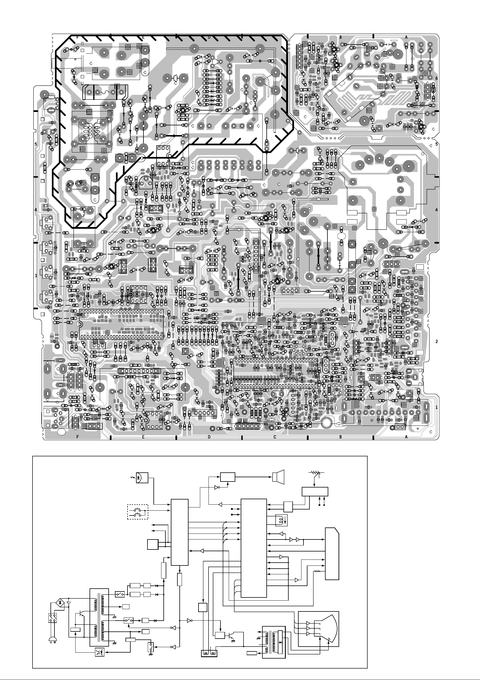
BLOCK DIAGRAM FOR EC8 CHASSIS
R715
Q711
Q711A
E
G-OUT
R711
Q721
Q721A
E
CL070
C721
R716
7
6
5
5
4
3
HIGH-VOLTAGE
K701-L
R703
C732
R732
R436
R452
D431
K7M
T451-3
R454
T451-2
T451-1
C421
R142
R140
CL040
C421H3
C421H2
R442
CL046
R152
J215
J216
R126
R122
X141
L205
C147
C134
L141
C136
C133
C106
J217
C425
X121
D1001
J212
T131
C132
CL039
AJ1
L442H1
KDY
KDY-1
JS442
CL042
C425A
KDY-3
C453
J301
KDY-5
D447
C1011
R449
KDY-6
Q445
R103
J201
J202
Q1006
JS1011
Q1011
J203
J211
KF
JS1002
J206
R1021
JS1101
R1001
C1001
1
C104
J208
J209
C112
CL047
TP-A
J104
L101
L102
D101
C511
CL043
J210
R127
R120
Q120
J213
R157
BT
IF
R100
R435A
R431
Q151
C148
JW10
1
5
R430A
J130
K7A
CL087
C641
J305
C201
CL080
C753
CL083
R752
R751
R744
PB701A
R713
D754
C711
CL081
R712
C752
R723
R722
J705
Q751
R721
R731
J701
R753
C741
JS741
J703
D752
CL079
C451
K7AA
D753
C751
D751
R742
D742
D741
R741
CL082
Q741
R453
R450
R435
R438
Q432H3
E
J501
J401
C431A
C431B
C431
R461
R455
B
C421H4
Q432H2
Q432H1
C441H3
C441H2
L432
C441
C421H1
C441H1
R513
R138
Q133
R135
R132
R137
Q131
L123
R128
L122
R129
L171
50
C124
J107
C153
R205
C152
C143
R145
JS113
C145
R147
Q142
X101
C131
C673
J214
Q132
JS131
R136
R133
C130
R134
R130
JS117
JS116
Q122
C129
L121
J218
C121
C120
Q121
J220
JS121
56
CL019
C122
C125
R121
R124
C127
R123
C137
L124
C135
1
C146
C126
C142
C141
C140
R139
R143
JS112
Q141
R149
R141
J110
PB101A
CL022
Q666
F601-A1
L601H3
L601H4
KL-2
C827
C818
J127
R022
Q012
C601A
C666
D666
C001
C003
CL024
L601
E
R832
SW601-H4
SW601-H3
C605
KL
R863
IC801
CL001
KAC-2
2
KAC
CL023
KAC-1
1
CL002
DANGER
LIVE
C607
C607H1
MAINS
D604
C604
C603Z
C606
D606
C605Z
2
R686
C608
C645
R681
C604Z
C606Z
R602A
R602H1
D605
R687
JS601
R602
JS602
1
C685
R602H3 R602H2
KL-1
R688
Q685
D685
VR641
R636
J408
D636
IC631
R663
D683
JS652
R661
C682
Q682
R667
R666
R691
C662
IC691
1
4
IC803
L801
R881
R873
CL007
J312
R880
R872
JS801
C801
CL008
8
C832
5
20
C835
C819
R831
9
C002
C004
C831
R843
R844
R845
40
R852
C811
R840
R011
C015
R013
R001
C807
R846
R828
C810
C829
C828
R839
C822
J830
R864
C812
R007
C012
R009
C013
C014
IC001
C016
J122
1
8
C006
Q611
C603
R623
R617
R620
D603
L615
C672
Q631
R631
C624
6
1
R639
JS654
D641
J407
C632
R633
R632
Q632
R638
C433
R672A
R672
IC671
4
D615
3
R689
JS653
Q686
J406
R635
Q661
E E
IC661
C671
L805
J311
L803
J309
28
C817
R838
C816
R842
29
C824
R874
J246
J241
J239
J238
J237
TP-C
C826
J240
C017
IC002
R004
1
D021
C011
Q021
C021
R021
D002
R008
C005
4
R002
C007
5
JW4
CL056
R146
R003
C008
J115
D635
JS651
D671
J119
C615
Q613H6
C613
C607H2
C614
R611
T611H2
T611H17
L635
D634
L634
C634
C635
D644
D643
R637
J404
R684
J306
CL029
D669
J310
J307
J308
D255
R875
J244
R1032
J243
J255
J242
R1031
R853
R254
J236
J234
C018
IC002H1
C663
J121
CL057
1
CL055
J118
C512
D1011
J235
J233
KCP
JW5
Q612
E
R615
R626
R622
D614
R619
D617
D618
D619
D616
R621
T611H5
5
L633
C633
D633
C644
R683
J402
J403
Q681
C501
R255
J254
R1030
D1012
R847
C513
R508
R506
R507
R505
CL044
D831
R235
R849
R236
R848
R237
R834
R833
CL059
D1013
CL058
CL045
JW6
5
R1028
R509A
R509
Q501
R504
R512
R1027
R217
R855
R854
R813
R216
C830
R857
C220
J114
C243
J117
J116
C246
CL049
J120
C618
C643
Q805
J232
28
C814
C813
L631
R248
R246
C241
R624
L501
C514
R856
C219
29
C242
KAA
R624Z
R625Z
D631
C502
C503
C504
R512A
J227
J229
C217
C218
C240
R245
J113
JS171
CL052
JW7
CL050 CL051
1
C617
R625
T611H8
T611H11
T611
C631A
C631
R652
C506
J304
J226
Q804
J230
J228
R214
R215
C216
R212
C244
R244
C247
L240
KA
C507
J231
Q613H5
L610
Q613H1
Q613
Q613H2
C616Z
C616
C616Y
Q613H3
Q613H4
C621
R628
R629
C438
R438A
R643
R642
Q651
R651
D501
C505
R501
R697
R502
IC501
J303
J224
J223
Q806
R206
R204
R859
C211
C213
J225
R213
C214
R243
C237
R241
R239
19
R242
R238
C232
R240
JS173
JS172
JW8
L241
L242
CL048
J128
J129
JW9
5
C434
Q435
D463
E
Q430
R433
R432
R434
L551
R430
Q431
C432
R696
D649
J221
J222
R203
JS151
R211
L202
C210
C212
R202
40
C209
C236
C235
IC201
C233
J302
R446
R437
R443
E
JW3
Q434
SW501
C128
R153
JS132
C251
L154
Q153
C151
Q201
R151
R154
J219
L201
C206
C208
C154
R201
C204
C202
C207
C203
C215
C205
C230
R234
C231
C234
R230
10
R158
X231
X132
C238
C144
JS111
J112
JW11
J108
J109
J106
L607
SW601
F601-A2
CL026
CL061
C601
SW601-H2
SW601-H1
F601
CL025
L601AH3
PB
L608
KSR
A1901
L601AH2
L601H2
J411
D1901
R1917
Q1902
D1902
C1900
R1907
L601H1
PS601A
L601AH1
CL028
L601AH4
CL027
L601A
C602
C602A
R601
2
CL030
KE-1 KE-2
KE
1
PS601
JS691
R1900
RL691
K1921
SW1902
SW1904
J252
R816
K1101
SW1901
J409
SW1903
J319
JWRR
L1923
C692
D691
R1901
Q691
R692
R645A
R1902
D646
R645B
R645
JS645
C693
R693
R646
J316
Q810
JS810
R1903
J317
J318
J251
R815
J249
J250
Q801
R858
R830
R806
R803
J320
1
CL004
56
J253
C837
L1106
C1107
R1106
J248
KH
KJ
1
1
R1922
R1921
C1921
R1111
J126
L1921
CL031
KX
1
JS1901
D692
R012
C1024
D645
Q802
R1904
C836
J410
J314
C691
J313
R861
CL060
D826
R862
10
R1910
R808
C833
C834
CL003
49
CL005CL006
X801
R822
R826
D1024
IC002H2
C1926
C1922
J123
CL053
J124
KSP
CL076 CL077
6
CAUTION
AT FOCUS PIN
C761
T451-4
CL038
CL041
L442
D482
C1015
R1008
R1010
R1025
KY
1
C103
C108
A101
G2
7
L442A
L442H2
R447
R1029
11
K7EM
T451
D445
Q1001
C1021
C110
8
T451-5
C1017
Q1007
Q1012
PB
C731
K7D1
CL075
8
K7D
9
9
CL073
10
CL072
C703
CL074
K701-M
CL086
R717
R725
CL088
L703
L702
R705
R704
R701
R702
C710
R714A
R724A
CL078
R714
R724
+B
CL084
1
L702A
K7B
L701
3
CL085
CL071
B-OUT
R704A
Q701
C701
Q701A
E
T451-7
T451-6
T451-11A
T451-10
C481
D481
R491
L1012
KEMC
3
KB
JS1001
CL010
JW2
CL
CL035
R451A
R448
CL014
C1016
R1015
CL016
C1012
R1013
J257
5
C1014
CL054
CL034
CL033
CL015
R1012
CL013
R1019
CL018
10
R1018
R1017
CL032
15
K1001
20
CL012
L1003
CL009
R1003
R1004
D1002
K1002
C1022
KEM
CL020
J101
C051
C100
CL021
AGC
C107
PB1
R451
TP-B
CL036
1
CL037
R482
D442
R481
C1013
C445
D446
Q1010
L1013
JWR
R1014
J204
R1011
D1010
R1009
D1008
L1010
D1007
R1016
R1007
R1005
CL017
D1003
R1006
KG
Q1008
C1010
CL011
R1002
R1026
1
Q1003
Q1002
J256
R1024
L1021
R1022
L1022
J102
C102
C101
J103
MB
DTA
C109
R102
R101
JW1
A1901
RC RECEIVER
KEY SW
SDA
SCL
IC803
MEMORY
D603-D606
SW901
AC
CONVERTER
C607
Q613
Q611
5
8
2
3
T611
16
17
11
15
13
12
D615
Q661
12V
Q651
Q631
IC671
IC601
Reg.
5V
9V
24V
115V
IC801
CPU
<ST92195B4B1>
RC-IN
1
8
KEY-IN
SDA
19
20
SCL
11
54
PROTECT
D671
D669
D649
Q682
Q685
Q686
MUTE
45
BLK
18
R
17
G
16
B
15
Q806
34
33
POWER
IC501
V-OUTPUT
<LA7832>
Q681
V-OUT
4
2
AUDIO-OUT
<TDA7231A>
Q012
Q142
V-FB
H-OUT
Q431
Q430
D.Y
IC001
2
4
3
SP902
IC201
IF/VIDEO/CHROMA/DFF
<TB1254N>
SCL
SDA
R
G
B
R/G/B-OUT
Q431
H-OUTPUT
4
34
35
15
16
17
18
26
25
32
20
21
22
6
7
50
51
56
54
48
46
41
43
39
38
49
53
T451 FLYBACK
CRT
HEATER
200V
IF-IN
SIF-IN
DET-OUT
TV-IN
EXT-IN
Q201
C-IN
Y-IN
SYNC-IN
SPEAKER
X132
L171
Pix
Q120
Q121
MONITOR
OUT
FOCUS/SCREEN
Q151
Q133
Q701
Q711
Q721
A101
TUNER
IF
TV-OUT
AUDIO-OUT
AUDIO-IN
BLK/R/G/B-IN
B
R
G
AERIAL
SCL
SDA
K1001
SCART
PICTURE
TUBE
H.V
Page 3
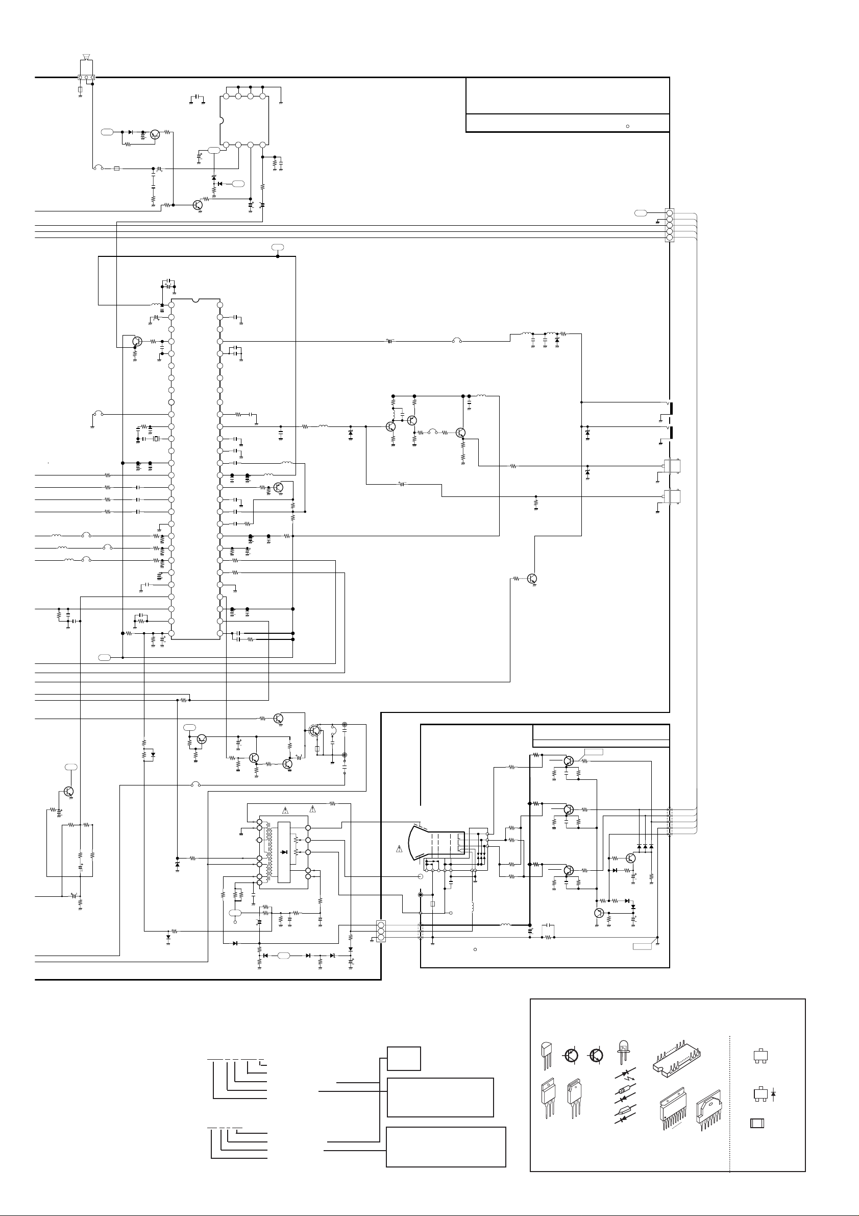
8. This circuit diagram covers a basic or representative chassis only. There may be
some components or partial circuit differences between the actual chassis and
the circuit diagram.
9. ■ Diode 1S1555 may be replaced with
1S2473, 1S2076 or DS472 unless otherwise noted.
■ Transistor 2SC536(Q,R,S),
2SC1740(Q,R,S), 2SC945A(Q,R,P) or
2SC1815(G,O,Y) unless otherwise
noted.
■ Transistor 2SA608(E,F) may be
replaced with 2SA933(Q,R),
2SA564(QA,RA), or 2SA1015(O,Y)
unless otherwise noted.
Expression of capacitance and resistance in circuit diagram.
Capacitance (Example)
1000 C M 2000 D
Characteristic
Capacitance value (220pF)
Tolerance (±20%)
Kind(Ceramic)
Rated voltage (1,000V)
Resistance (Example)
1/2 N J 1.2
Resistance value (1.2Ω)
Tolerance (±5%)
Kind (M.carbon)
Rated wattage(1/2W)
D : Carbon
N : Metallized carbon
S : Oxide metallized
W : Wire wounding
C : Solid
T, A, U, D : Electrolytic
C, K, B : Ceramic
F : Mylar film
M, N : Polypropylene
Z : Metallized paper
J= ± 5%
K= ± 10%
M= ± 20%
Terminal guide
C : Collector
B : Base
E : Emitter
A : Anode
K : Kathode
Chip Components
SP901
A10B12500
Q901
A33LPE02X01
<EKRANAS>
270
R212
1/16GJ1KC
R211
KZ0.01GQF
C205
KZ0.01
GQF
C204
+5V
1/16GJ100C
R234
1/16GF
5.6KC
R245
EM1
C1001
2SJ56
R430
1/16GZ
0C
R461
1/16GJ
390C
R437
MTZJ8.2A
D446
2400010
T451-11A
T451
L40B12200
1
2
3
4
5
6
710
11
T451-2
2400030
2400010
T451-7
2400010
T451-10
T451-5
2400010
T451-1
2400030
Q432H3
2400010
2400010
2400010
L432
J
D482
1SS133
:1SS176
R482
6.8K
R481
DJ150K
D481
EU1
R447
4.7K
PRO
TECT
D445
1SS133
:1SS176
R448
1/2DJ
330
D442
1SS133
C445
EM10
C421
1500MH
7500XK
115V
R436
DJ10K
D431
RD9.1EB1
:RD9.1EB2
:MTZJ9.1A
:MTZJ9.1B
R452
J
C451
100EM
2.2X
DJ680K
R454
1K
R453
BU808
DFI
Q432A
EM47CD
C434
AH
Q431
200MJ
0.39UCQ
C441
IC201
1
2
3
4
5
6
7
8
9
10
11
12
13
14
15
16
17
18
19
20
21
22
23
24
TB1254N
25
26
27
28 29
30
31
32
33
34
35
36
37
38
39
40
41
42
43
44
45
46
47
48
49
50
51
52
53
54
55
56
16EM10
C140
L124
J
C135
KZ0.01
GQF
X231
V10B2960N
C232
CC10CGQ
R230
1/16GJ
33KC
R246
1/16GJ
27KC
C220
16KZ1FA
R216
1/16GJ
10KC
C219
KK5600GQ
1/16GJ
100C
R215
R214
1/16GJ
100C
25KZ0.1GQF
C209
16KK0.22
BA
C203
1/16GJ
150C
R201
R217
1/16GJ
10KC
C206
KZ0.01GQF
1/16GJ100C
R237
R236
1/16GJ100C
1/16GJ100C
R235
25KZ0.1GQF
C237
C236
25KZ0.1GQF
25KZ0.1GQF
C235
R238
1/16GJ
100C
L241
L2B9100KN
1/16GJ
100C
R240
R242
1/16GJ
100C
L2B9100KN
L240
L242
L2B9100KN
R248
1/16GJ
56KC
C242
FK0.047
(BE:D)
C122
25KZ
0.1GQF
C241
63GJ0.47V:
HJ0.47
C231
KK2200
GQ
C217
16EM
470CD
C218
KZ0.01GQF
R213
1/16GJ
220KC
C216
EM1
C213
16EM10
C214
KZ0.01
GQF
C207
KZ0.01GQF
C208
16EM47
C233
16EM47
C234
25KZ0.1GQF
R239
1/16GJ
2.2KC
R241
1/16GJ
2.2KC
R243
1/16GJ
2.2KC
R
G
BLK
B
HV
IF Vcc
RIPPLE
FIL
SIF OUT
AUDIO
OUT
IF GND
IF IN
IF IN
EXT
AUDIO
IF AGC
APC
FILTER
X’TAL
CW OUT
RGB VCC
(9V)
Ys/Ym SW
EXT.R IN
EXT.G IN
EXT.B IN
Y/C GND
R OUT
G OUT
B OUT
ref R
V RAMP
V NFB
V OUT
ABCL IN
FBP IN/
SCP OUT
H AFC
FILTER
H Vcc
(9V)
H OUT
Dig. GND
SCL
SDA
BLACK Det
Dig. VDD
SYNC IN
Y IN
DC
Restor
M OUT
Y/C Vcc
(5V)
C IN
U IN
V IN
EXT IN
LOOP
Filter
TV IN
DE-EMP./
Mon OUT
PIF tank
PIF tank
DC NF
H CORR.
IN
IF DET
OUT
AFT OUT
SIF IN
ABL IN
IK IN
L201
J
RF_AGC
+9V
+9V
C146
16EM47
T451-4
2400010
T451-3
2400010
T451-6
2400010
C230
16KK
0.22BA
R239/41/43
R238/40/42
1SJ2.2
R509A
25EM
2200CD
C512
C513
EM33
R507
82
R508
2.2K
R506
1.5K
R505
5.6K
C514
EM10
R504
1/16GJ
56KC
PRO
TECT
Q501
AH
1
+9V
1AA0B10H055AA ASSY, PWB, MAIN, C3MWW
R450
15K
R434
1/16GJ
10KC
C240
KK2200GQ
C450
X
C244
KK0.01
GQ
R244
1/16GJ
330C
C243
KK1800
GQ
R255
X
R254
220K
C247
J
C421H4
2400030
C421H3
2400030
C441H1
2400030
C441H3
2400030
D463
1SS133
L205
L2B94R7KN
C425
3000KK680
(CRD:NH)
R202
1/16GJ
470C
R203
1/16GJ1KC
Q201
AJ
R204
1/16GJ1KC
R205
1/16GJ270C
R145
100
Q142
AH
R146
1/16GJ
1KC
C008
EM1
IC001
TDA7231A
1234
5678
R002
1/16GJ
39KC
R003
1/16GJ
6.8KC
C007
KK2200
GQ
C002
16EM
470
C003
16KK0.22
BA
C004
16KK0.22
BA
R001
2.2
C001
16EM1000
12V
KSP
J10EA030N
JS1901
1/16GZ0C
R438
2SJ3.9
C453
100EM
22
AJ1
J
JS171
1/16GZ0C
JS172
1/16GZ0C
JS173
1/16GZ0C
C125
16KZ2.2
(FA:GWF)
C210
16KZ1FA
C212
16KZ1FA
R435
X
Q430
STX112
R432
1/16GJ
1KC
R433
1/16GJ390C
PRO
TECT
D646
J
R646
X
1SS133
D645
C431
250GJ0.47
JS442
J
R451A
1SJ0.22
R491
1/2DJ
2.2B
KB
J11SG030N
1
2
3
KA
J11SG050N
1
2
3
4
5
1AA0B10E2950A PWB, MAIN, C3LC
FOCUS
SCREEN
PB101
AA4B10H00400:
AA4B10H0040A
Q434
2SA984
(E:F)
R443
1/16GJ
390C
R446
1/16GJ
2.2KC
Q435
AH
R431
6.8K
R012
10K
Q012
AH
R013
1/16GJ3.3KC
C006
10EM
100
C215
CJ82
CGQ
C141
CJ100
CGQ
D255
J
R455
DJ680K
L202
J
R022
10K
Q021
AJ
R021
10K
D021
1SS133
C021
10EM220CD
+9V
D1001
MTZJ11C:
RD11EB3
R206
1/16GJ
470C
C127
16KZ2.2
(FA:GWF)
Q1010
AH
R1014
1/16GJ
5.6KC
TP-B
J30B0250N
C137
KZ0.01
GQF
J123
ZZ0122
J124
J
C017
KZ0.01F
C432
10EM470CD
C1011
EM4.7
AUDIO IN
VIDEO OUT
VIDEO IN
AUDIO OUT
Q170
AH
R130
1/16GJ
470C
L122
100C
R128
1/16GJ
1KC
Q131
AJ
R132
1/16GJ
1KC
R134
1/16GJ
1KC
Q133
AH
R137
1/16GJ
470C
R177
1/16GJ
470C
R1002
75
L1010
L2B94
R7KN
L1013
L2B94R7KN
C1017
KK1000
GQ
C1013
CJ100
CGQ
R1012
1/16GJ
100C
R1003
75
L123
L2B9220KN
K1001
1AV4J31B00800
K1002
1AV4J11B3060N
BNC_J
X
C129
X
D1003
MTZJ11C:
RD11EB3
D1004
MTZJ11C:
RD11EB3
D1002
MTZJ11C:
RD11EB3
JS1101
L2B94
R7KN
R133
1/16GZ
0C
JS131
1/16GZ
0C
R136
1/16GZ
0C
C128
10EM
220CD
1AA0B10H055AA ASSY, PWB, MAIN, C3MVW
1AA0B10H055AA ASSY, PWB, MAIN, C3MSW
C144
J
AT1
Q721
R724
2SJ
15K
Q711
R714
2SJ
15K
R715
X
Q701
1/2DJ
2.7K
R705
R732
X
G-OUT
R-OUT
B-OUT
5
1
K701-L
J11B3140N
275910
8
6
11
-41
C731
2000KP
1000
AHE:
2000KZ
1000HE
K7D
X
K7M
J30B0250N
TP-7B
TP-7E
1
3
R704
2SJ
15K
K7A
J11SG
050N
K7B
J11SG
030N
Q701A,Q711A,Q721A
C732
KK560
L701
J
1/16GJ
470C
R703
R713
1/16GJ
470C
1/16GJ
470C
R723
R702
X
1/16GJ
220C
R701C701
KK820
GQ
KK820
GQ
C711
R711
1/16GJ
220C
X
R712
R722
X
1/16GJ
220C
R721
C721
KK820
GQ
R741
1/16GJ
1.2KC
Q741
AJ
R742
1/16GJ
12KC
1/16GJ
680C
R744
L702
J
D742
J
D741
J
C741
X
R725
X
R753
1/16GJ
10KC
C751
16EM
330CD
D751
1SS133
R752
1/16GJ
10KC
R751
1/16GZ
0C
1SS133
D754
D753
1SS1331SS133
D752
Q751
AJ
C710
X
1AA0B10H055AB
ASSY,PWB,SOCKET,C3MWW
Q721A
X
Q711A
X
Q701A
X
R717
1/2DJ
2.7K
R716
1/2DJ
2.7K
R704A
X
R714A
X
R724A
X
K7D1
J30B
0250N
L703
J
PB701
A4B10E29500:
A4B10E2950B
QT0193Z:
2SC2228
(D:E)
B
B
C
E
E
C
B
B
E
C
C
E
B
C
E
K
K
A
K
A
A
N/2
1
N/2 + 1
N
10
9
3
2
1
7
6
5
4
3
2
1
Transistor
B
Diode
A
Resistor
123
C
E
K
12 x 103= 12k
Page 4
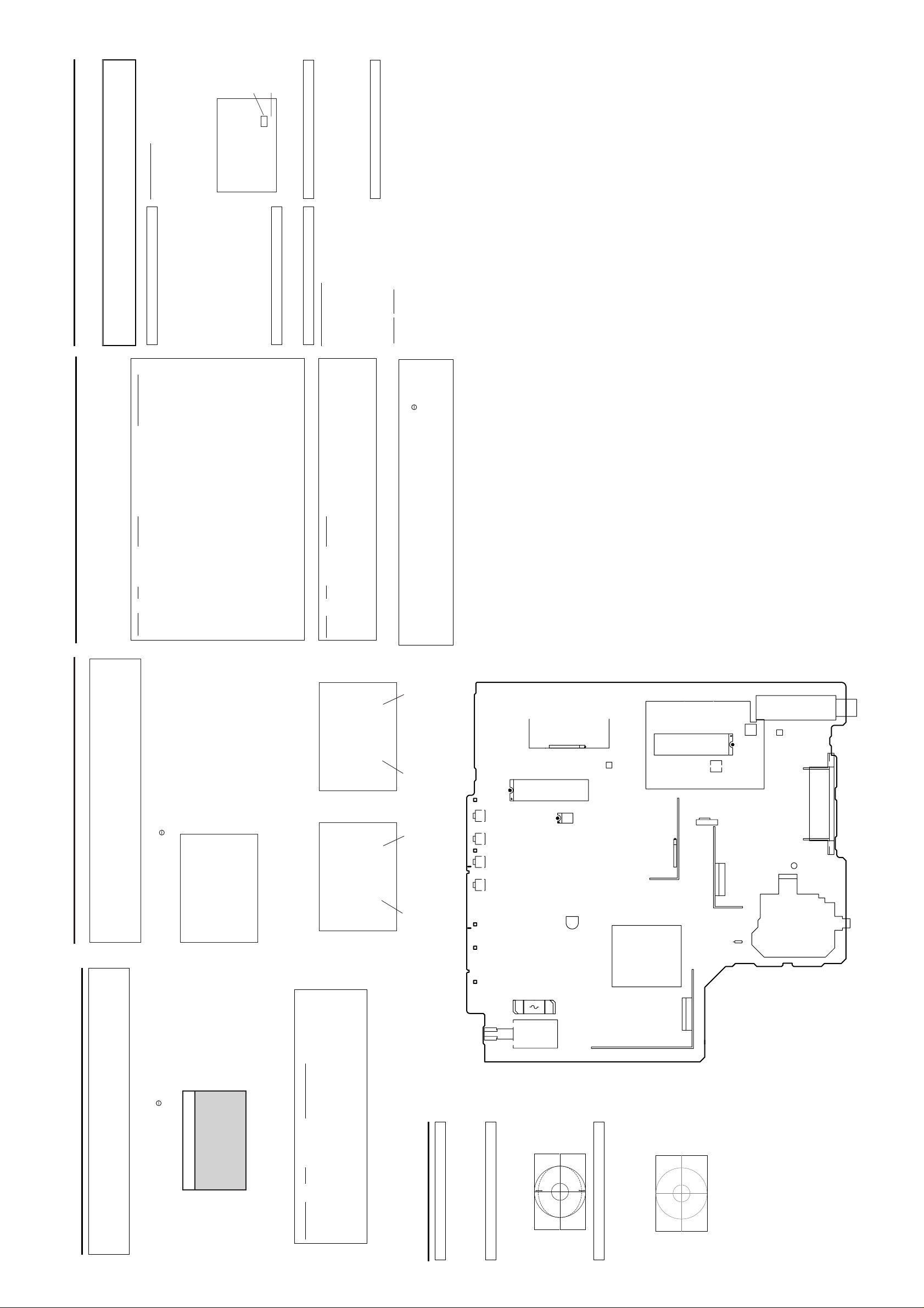
SERVICE ADJUSTMENTS
Main Board
Component Location
TELETEXT ON
ON TIMER ON
Wel.TEXT ON
P&P ON
SORTING AUTO
DESTINATION UK
(NOT APPLICABLE)
[ADJUSTMENTS]
For how to adjust the each service data, please see “SERVICE ADJUSTMENT “ for entering the service
mode, selecting service item and adjusting the service data value.
IMPORTANTNOTICE
Do not attempt to adjust the following service adjustments except those requiring readjustments in servicing
otherwise it may cause loss of performance and product safety.
white balance by using LEVEL+ or LEVEL - button.
DRIVE ADJUSTMENT
5. Receive the white raster signal.
6. Select item “03 GRY”.
7. Adjust [R-Drive] and [B-Drive] control to obtain proper
+B ADJUSTMENT
1. Receive white raster pattern.
2. Set controls to normal.
3. Connect a digital voltmeter to test point “TP-B” and
P▼ button.
LEVEL - button.
a) Select [R-Drive] or [B-Drive] by using the P▲ or
b) Adjust [R-Drive] or [B-Drive] by using the LEVEL+ or
GND.
4. Adjust voltage to 100 ±0.5V by using VR641 (14”).
4. Adjust voltage to 115 ±0.5V by using VR641 (21”).
[R-Drive]
[B-Drive]
3F
Adjustable Range:
00 ~ 3F ~ FF
Regular
03 GRY 3F
HORIZONTAL PHASE ADJUSTMENT
and select item “01 AGC”.
to be 3.2Vdc.
551.25MHz with 63dBuV/75Ω terminated signal gain.
RF-AGC ADJUSTMENT
1. Input and tune an RF signal which is UHF ch31
2. Connect digital voltmeter to test point TP-A and GND.
3. Enter the service mode and select mode “Regular”,
4. Press the LEVEL+ or LEVEL - button to adjust voltage
GREY SCALE ADJUSTMENT
FOCUS ADJUSTMENT
By using FOCUS VR, adjust focus control for well defined
scanning lines.
“02 P H-P”.
horizontal centre.
1. Receive circular pattern .
2. Enter the service mode and select mode “Image”, item
3. Press the LEVEL+ or LEVEL - button to adjust
ADJUSTMENT
item “02”. The horizontal line will appear on the
screen.
1. Select AV mode with no signal input.
CUT-OFF
colour to be just visible.
2. Enter the service mode and select mode “Regular”,
3. Adjust the Screen VR on the FBT to obtain the one
4. By using the buttons 1, 2, 4, 5, 7, 8 on the remote
HIGH-VOLTAGE CONFIRMATION
control, adjust the line to be white.
1. Receive circular pattern.
The key allocation is as follows;
and a high voltage meter to CRT anode.
current reading 0.6mV (14”).
2. Connect a digital volt-meter to both terminals of 453,
Button No. Operation
current reading 1.1mV (21”).
3. Confirm high voltage to be 20.5KV ± 1 KV at beam
3. Confirm high voltage to be 25.3KV ± 1 KV at beam
1 Increase Red
2 Decrease Red
4 Increase Green
5 Decrease Green
7 Increase Blue
8 Decrease Blue
Item No. OSD Description Suggested Settings
01 P V-P PAL Vertical position adjustment 02
02 P H-P PAL Horizontal position adjustment 0D
03 P V-L PAL Vertical linearity adjustment 09
04 P VSC Vertical s-correction adjustment 07
05 P V-S Vertical size adjustment 24
06 P V-P Wide vertical position adjustment 02
07 P H-P Wide horizontal position adjustment FF
08 P V-L Wide vertical linearity adjustment 00
09 P VSC Wide vertical s-correction adjustment 00
10 P V-S Wide size adjustment F0
11 N V-P NTSC vertical position adjustment FE
12 N H-P NTSC horizontal position adjustment 03
13 N V-L NTSC vertical linearity adjustment 00
14 N VSC NTSC vertical s-correction adjustment 00
15 N V-S NTSC vertical size adjustment 01
16 N V-P NTSC wide vertical position adjustment 00
17 N H-P NTSC wide horizontal position adjustment 00
18 N V-L NTSC wide vertical linearity adjustment 00
IMPORTANTNOTICE
Do not attempt to change the data value of service items not listed below table otherwise it may cause loss of
performance and product safety. If you can not restore the data value of each service item, please initialize the
memory IC following to the below description INITIALIZATION OF MEMORY IC and re-adjust all of service
ADJUSTABLESERVICE ADJUSTMENT
SERVICE ADJUSTMENTS
adjustments.
[Image]
19 N VSC NTSC wide vertical s-correction adjustment 00
20 N V-C NTSC wide vertical size adjustment F0
Item No. OSD Description
01 AGC AGC Adjustment
[Regular]
Regular mode
02 -- Cut-off Adjustment
03 GRY Grey Scale Adjustment [White Balance]
04 CTR Contrast Adjustment (Factory use, use default setting data)
05 -- Screen adjustment (Factory use, use default setting data)
06 OSD On-screen Display Positioning Adjustment
Regular
[INITIALIZATION OFMEMORY IC]
To initialize the memory IC (IC803), press and hold the NORMAL button and then press the button on the
front control panel, and then turn the Mains switch Off and On. Now the initialization is completed.
When the memory IC has been initialized all of the setting data (option setting data and service adjustment data)
Exit from the Service Mode
+ Press the MENU button or turn off the TV set by using the Mains switch.
stored in the IC are reset to the default value. It is necessary to set the option setting and readjust the service
Adjustment Data
01 AGC 2A
Adjustment No.
and Item name
adjustments listed on the above.
IC801
IC002
TP-C
IC201
L171
T131
A101
TP-A
Note: Some items of the service adjustments for this chassis are controlled by the CPU, IC801, and the
[SERVICE ADJUSTMENT]
SERVICE ADJUSTMENTS
IMPORTANTNOTICE
Do not attempt to adjust service adjustments not listed below as it may cause loss of
performance and product safety.
adjustments are carried out by using the RC handset.
on the screen.
To enter the Service Mode
+ Press and hold the “GREEN” button and button on front control panel. The adjustment item will be displayed
The available adjustment items are as follows;
TELETEXT OFF
Image : This can be adjusted for picture images/shapes.
Regular : This can be adjusted for the service adjustment.
other : This is for the factory setting. Do not adjust.
TB1254 : This is for the factory setting. Do not adjust.
Image
ON TIMER OFF
Wel. TEXT ON
P&P ON
SORTING AUTO AUTO
DESTINATION UK
the TV set may not operate properly.
* Do not adjust items in the “other” and “TB1254” otherwise
the Volume + (RIGHT) button.
To select the mode and service item and change data value
+ Select the desired adjustment mode (Image or Regular mode ) by using the P▲ or P▼ button and then press
SW1904
Adjustment Data
SW1902 SW1903
Image mode
01 P V-P 05
Image
Adjustment No.
and Item name
+ To select the adjustment item, use the P▲or P▼button.
+ To change the service data, use the Volume -(LEFT) or Volume + (RIGHT) button.
+ The data which is set in the service mode is stored into the memory IC automatically.
SW1901
IC803
VR641
IC501
SW501
Q432A
R453
TP-B
T451
T611
F601
Q613
SW601
[After replacing the Memory IC (IC803)]
The memory IC, IC803, stores the feature setting data of TV set and service adjustments data for each circuit,
therefore, when the memory IC is replaced, it should be programmed by following “OPTION SETTING” and
SERVICE ADJUSTMENTS
“SERVICE ADJUSTMENT”.
window will appear on the screen. (Options required for this model are shown below)
[OPTION SETTING]
To enter the Option Mode
+ Press and hold the F/OK button on the remote control and button on the front panel of the TV. The option
CE14M4-B
CE14M4SL-B
To set the Option Mode
+ Select the desired option item by using the P▲ or P▼ button .
+ To switch the option mode, use the Volume - (LEFT) or Volume + (RIGHT) button.
+ The data which is set in the option mode is stored into the memory IC automatically.
Option Mode Mode Description & Note
The following table shows the available option items and default setting modes.
TELETEXT ON or OFF Teletext available, default “ON”
ON TIMER ON or OFF On-timer available, default “ON”
Wel. TEXT ON or OFF Plug & Play mode, default “ON”
P&P ON or OFF Display message when first set up, default “ON”
SORTING AUTO Sorting or Tuning Tuning mode option, default “SORTING”
DESTINATION UK or IRE Destination option , default “UK”
Exit from the Option Mode
+ Press the MENU button or turn off the TV set by using the Mains switch.
“01 P V-P”.
VERTICAL PHASE ADJUSTMENT
SERVICE ADJUSTMENTS
1. Receive circular pattern..
2. Enter the service mode and select mode “Image, item
centre.
VERTICAL SIZE ADJUSTMENT
3. Press the LEVEL+ or LEVEL - button to adjust vertical
1. Receive circular pattern .
2. Enter the service mode and select mode “Image”, item
“05 P V-S”.
vertical height.
3. Press the LEVEL+ or LEVEL - button to adjust the
❚❚❚❚❚❚❚❚❚❚❚❚❚❚❚❚❚❚❚❚
and select item “06 OSD”. The OSD test bar will
appear on the top of screen.
2. Enter the service mode and select mode “Regular”,
3. Press the LEVEL+ or LEVEL - button to adjust proper
OSD positioning.
OSD POSITIONING ADJUSTMENT
1. Receive circular pattern.
 Loading...